Note: Descriptions are shown in the official language in which they were submitted.
CA 03088091 2020-05-13
WO 2019/098999
PCT[US2017/061717
1
PULSE WIDTH MODULATION CONTROL FOR A MULTILEVEL
CONVERTER
BACKGROUND
1. Field
[0001] Aspects of the present disclosure relate to a multilevel power
converter,
particularly to pulse width modulation control of a multilevel power
converter. A power
converter may also be referred to as "drive", "drive system" or "power supply"
and
throughout the specification these terms can be used interchangeably.
.. 2. Description of the Related Art
[0002] Multilevel power converters are used for example in applications
of medium
voltage alternating current (AC) drives, flexible AC transmission systems
(FACTS), and
high voltage direct current (HVDC) transmission systems, because single power
semiconductor devices cannot handle high voltage. Multilevel converters
typically
.. include a plurality of power cells for each phase, each power cell
including an inverter
circuitry having semiconductor switches that can alter the voltage states or
levels of the
individual cells. Depending on the type of inverter circuitry used, e.g., half-
bridge or full
bridge, each power cell may have one or more switching legs. By controlling
switching
events of the individual switching legs of each power cell, it is possible to
control the
voltage across each cell and resultantly obtain an AC output waveform having
multiple
discrete voltage levels. A multilevel converter is often described by the
number of
discrete levels in output voltage waveform.
[0003] In certain applications, it may be desirable to control the
switching events in a
multilevel converter using pulse width modulation (PWM). A PWM based control
provides several benefits, especially a reduction in the harmonic spectrum at
every level.
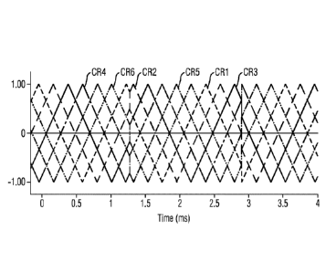
Multilevel converters typically use phase-shifted triangular carriers at the
heart of the
CA 03088091 2020-05-13
WO 2019/098999
PCT[US2017/061717
2
PWM method. A conventional method used for multilevel converters, particularly
those
having a cascaded H-bridge topology, is phase-shifted pulse width modulation
(PSPWM)
carrier method. In the PSPWM method, a reference signal for each cell, which
is typically
a sine-waveform, is compared against a triangular carrier to obtain the
switching
instances for a first switching leg of the cell. Typically, each cell has its
own triangular
carrier. In the PSPWM method these carriers are phase-shifted. The same
reference sine-
waveform is compared against the inverted triangular carrier to obtain the
switching
instances for the second switching leg of the same cell.
[0004] But the conventional PWM methods, such as those mentioned above, do not
provide an optimum spectrum for line-line output voltage. The quality of the
output
voltage deteriorates especially at high output voltage frequency, or when the
converter
has a low number of levels. If the output voltage frequency is high and the
converter has
a reduced number of levels, an obvious option is to increase the switching
frequency. But
increasing the switching frequency also increases the overall losses.
SUMMARY
[0005]
Briefly, aspects of the present disclosure relate to a multilevel power
converter
and further to pulse width modulation control of a multilevel power converter.
[0006] A first
aspect of the present disclosure provides a method for controlling
multiple switching devices of a multilevel converter comprising providing a
plurality of
carrier signals and a reference signal, the reference signal comprising a
waveform range
divided in a plurality of contiguous bands, dynamically allocating the
plurality of carrier
signals to the multiple switching devices, and generating pulse width
modulation signals
to generate switching events of the multiple switching devices based on a
comparison of
dynamically allocated carrier signals with the reference signal, wherein the
plurality of
carrier signals comprises a phase shift between the carrier signals, and
wherein the
plurality of carrier signals are dynamically allocated to the multiple
switching devices
such that for each switching device the plurality of carrier signals are
rotated and selected
based on a position of the reference signal with respect to the plurality of
bands.
CA 03088091 2020-05-13
WO 2019/098999
PCT[US2017/061717
3
[0007] A
second aspect of the present disclosure provides a multilevel converter for
producing a multiphase AC power supply, comprising a plurality of power cells
for
supplying power to one or more phases, each power cell comprising multiple
switching
devices incorporating semiconductor switches, and a pulse width modulation
controller
connected to each of the power cells for controlling a voltage output of the
plurality of
power cells by controlling a switching event of each of the switching devices
by pulse
width modulation, wherein the pulse width modulation controller is configured
to
dynamically allocate a plurality of carrier signals to the multiple switching
devices, and
generate pulse width modulation signals to generate switching events of the
multiple
switching devices based on a comparison of dynamically allocated carrier
signals with a
reference signal, wherein the plurality of carrier signals comprises a phase
shift between
the carrier signals, and wherein the plurality of carrier signals are
dynamically allocated
to the multiple switching devices such that for each switching device the
plurality of
carrier signals are rotated and selected based on a position of the reference
signal with
respect to the plurality of bands.
BRIEF DESCRIPTION OF THE DRAWINGS
[0008] FIG. 1
is a schematic diagram illustrating a cascaded three-phase H-bridge
multilevel converter having three cells/phase topology in accordance with an
exemplary
embodiment of the present disclosure.
[0009] FIG. 2 illustrates a graphical representation of a band arrangement
and a
modulating reference waveform in accordance with an exemplary embodiment of
the
present disclosure.
[0010] FIG. 3
illustrates a graphical representation of a simulated triangular carrier
arrangement with carrier signals through in accordance with an exemplary
embodiment
of the present disclosure.
[0011] FIG. 4
illustrates a graphical representation of a simulated carrier
arrangement with rotating carrier signals using a proposed PSPWM method with a
CA 03088091 2020-05-13
WO 2019/098999
PCT[US2017/061717
4
modulation index of 1 in accordance with an exemplary embodiment of the
present
disclosure.
[0012] FIG. 5
illustrates a schematic of an example of a finite state machine which
dynamically allocates carrier signals for all the switching devices of each
switching leg
for a cascaded H-bridge multilevel converter having a three cells/phase
topology, in
accordance with an exemplary embodiment of the present disclosure.
[0013] FIG. 6
illustrates a schematic of state transitions based on a proposed carrier
allocation method for a cascaded H-bridge multilevel converter having a three
cells/phase
topology, in accordance with an exemplary embodiment of the present
disclosure.
[0014] FIG. 7 illustrates a graphical representation of pulses obtained
using a
proposed carrier allocation method for a sinusoidal reference signal in
accordance with an
exemplary embodiment of the present disclosure.
[0015] FIG. 8
through FIG. 13 illustrate simulation results demonstrating differences
in quality of output voltages and currents obtained by the proposed modulation
method in
comparison to a conventional PSPWIVI method for a cascaded H-bridge multilevel
converter with three cells per phase in accordance with an exemplary
embodiment of the
present disclosure.
[0016] FIG. 14
illustrates a modular multilevel converter (M_MC) that includes a
PWIVI controller in accordance with another embodiment of the present
disclosure.
[0017] FIG. 15 illustrates a graphical representation of simulated line-
line voltage
spectrum for a modular multilevel converter as illustrated for example in FIG.
14 using a
proposed selective PSPWM in accordance with an exemplary embodiment of the
present
disclosure.
DETAILED DESCRIPTION
[0018] Embodiments of the present disclosure relate to a new pulse width
modulation
86336711
(PWM) method which can be, in principle, used for many different types of
multilevel
converters. In general, a multilevel converter may have one or more phases,
including a plurality
of power cells for each phase. Each power cell includes an inverter circuit
having one or more
switching legs provided with switching devices, which can alter the voltage
states or levels of
5 the individual cells. By controlling switching events of the individual
switching legs of each
power cell, it is possible to control the voltage across each cell and
resultantly obtain an AC
output waveform having multiple discrete voltage levels.
[0019]
While the embodiments of the present invention have been illustrated for
certain
exemplary multilevel converters that can be used in industrial applications,
it is to be understood
that the proposed PWM controller and its underlying methods of operation are
not limited to
the herein described types of multilevel converters, but can be generalized
for multilevel
converters with any number of cells or to many other multilevel topologies.
[0020]
In a first embodiment, a proposed modulation method is illustrated for a
cascaded H-
bridge multilevel converter. An example of such a converter is the Perfect
Harmony GH180 0
drive manufactured by Siemens Industry, Inc.
[0021]
FIG. 1 illustrates a schematic of an embodiment of a system 1 comprising
cascaded
H-bridge multilevel converter 10 having a seven-level topology, including
three phases with
three power cells per phase, which additionally incorporates a PWM controller
30 in accordance
with an aspect of the present disclosure. The topology of the present
embodiment of the
multilevel converter is described for example in U.S. Patent No. 5,625,545 to
Hammond..
[0022]
In the example of FIG. 1, the system 1 is a medium voltage drive comprising a
three-phase power source providing a power input 2 via lines Li, L2 and L3.
The multilevel
converter 10 is connected to the AC power input 2 and produces a three-phase
AC power supply
as output 3, via phase output lines u, v and w. The AC output 3 can be
Date Recue/Date Received 2021-09-29
CA 03088091 2020-05-13
WO 2019/098999
PCT[US2017/061717
6
connected to a load 20, which in this example comprises a motor. The motor 20
may be
operated by controlling the frequency and/or amplitude of the output voltage
produced by
the multilevel converter 10.
[0023] Each
phase of the multilevel converter 10 comprises a respective phase leg 11
formed from a plurality of power cells 12 arranged in a cascaded manner. In
the example
of FIG. 1, the phase legs 11 are each formed from the same number of power
cells 12,
namely three, that are connected in series. Each power cell 12 of a phase is
connected to
the power input 2 via respective input lines Li, L2 and L3. Power to the input
lines Li,
L2, L3 may be provided, for example, via a multi-phase winding transformer.
The power
cells 12 of the three phases are respectively labelled as cell A1 through cell
A3, cell B1
through cell B3 and cell C1 through cell C3. Each power cell 12 is responsive
to control
signals from the PWM controller 30 to alter the voltage level and/or frequency
output,
resulting in a multilevel voltage waveform for each phase. The power cells 12
generally
include power semiconductor switching devices, passive components (inductors,
capacitors), control circuits, processors, interfaces, and other components
for
communicating with the controller 30. The power cells 12 operate based on
signals from
the controller 30.
[0024] Each of
the power cells 12 include single-phase inverter circuitry connected to
separate DC sources produced by a rectification of the AC power input for each
power
cell 12 via input lines Li, L2, L3. In this example, the rectification is
carried out by diode
rectifiers 13a-f arranged in a bridge rectifier configuration. The present
example also uses
filtering circuitry including, for example, a capacitor 14, for smoothing out
voltage
ripples from the rectified DC power.
[0025] The
inverter circuitry of each cell 12 comprises power semiconductor
switching devices 15a-d arranged in an H-bridge, also referred to as full
bridge,
configuration. The switching devices 15a-d may include, for example and
without
limitation, power transistors such as insulated-gate bipolar transistors
(IGBT). The
switching devices 15a, 15b connect to cell output line 16a while the switching
devices
CA 03088091 2020-05-13
WO 2019/098999
PCT[US2017/061717
7
15c, 15d connect to cell output line 16b. The transistors 15a-d receive pulse
width
modulation signals, for example, in the form of gate input signals 18
controlled by the
controller 30 based on pulse width modulation. The controller 30 selects
either of
transistors 15a or 15b to be ON via a first switching leg 17a, and either of
transistors 15c
or 15d to be ON via a second switching leg 17b, which will permit power to
pass to the
load 20 by way of the line 16a or 16b respectively. In other words, a
controller triggered
switching event of the switching leg 17a causes one of the transistors 15a,
15b to be in an
ON state and the other to be in OFF state. Likewise, a controller triggered
switching
event of the switching leg 17b causes one of the transistors 15c, 15d to be in
an ON state
and the other to be in OFF state. In the embodiments illustrated, the
switching legs 17a,
17b of an individual cell 12 are simply referred to as switching leg A and
switching leg B
of that individual cell 12.
[0026] Each of
the power cells 12 may be constructed internally to low-voltage
standards, despite its inclusion in a medium-voltage apparatus drive 1. By way
of
example, each power cell 12 may have a 600-volts rating. Thus, the maximum
voltage
level that can be output by each of power cells 12 is about 600 VDC. Depending
on
which transistors are ON, the output voltage across the cell output lines 16a,
16b of each
power cell 12 may be of either polarity or zero. Thus, each power cell 12 can
have three
output states: +600 VDC, -600 VDC, or ZERO VDC. Due to the serial connection
between three power cells 12 in each phase output line, such as, for example,
cells Ai, A2,
A3 to the phase output line u, it is possible to produce a maximum output
voltage
magnitude of about 1800 VDC for the respective phase output line. Each power
cell 12
may be operated independently of another. Therefore, it is possible to provide
at least
seven voltage levels per phase to motor 20. The approximate values of these
line-neutral
voltage states include +/-1800 VDC, +/-1200 VDC, +/-600 VDC and ZERO VDC. In
general, a cascaded H-bridge multilevel converter having N number of power
cells 12 per
phase is capable for producing Ni. number of line-neutral voltage states for
each phase,
where NL=2N+1. It should be noted that the line-line voltage may have more
levels than
the phase (line-neutral) voltage. For example, a cascaded H-bridge multilevel
converter
may have 2NL-1 levels in the line-line voltage. Other topologies may have
different
CA 03088091 2020-05-13
WO 2019/098999
PCT[US2017/061717
8
number of levels depending on the modulation technique used.
[0027] The motor 20 may comprise any type AC-type motor, for example,
synchronous, asynchronous, permanent magnet, and may be rated for low voltage,
medium voltage or high-voltage. For example, medium-voltage AC motors, such as
those
used in industrial process control, may operate in the 4.16kV to 13.8kV range.
Greater or
lesser voltage may be used. More than one motor 20 may be connected. Other
loads may
be used instead of or in addition to the motor 20. The motor 20 responds to
the voltage
applied by the multilevel converter on the three phases, for example, to
increase, decrease
or maintain a speed or position.
1 0 [0028]
The controller 30 may comprise, for example, a processor with a memory for
storing and executing specific instructions to implement the illustrated PWM
control. The
controller 30 may be constructed, for example and without limitation, by a
microcontroller with internal or external memory, or by a fixed-point or
floating-point
digital signal processor (DSP), or by a programmable logic device (PLD), or
any
combination of the above mentioned. By pulse-width modulating the voltage
reference
for each phase, the controller 30 controls each of the power cells 12, and
thus, the
amplitude and frequency of the voltage output between the output lines 16a,
16b of each
power cell 12. A control circuit or control board in the power cells 12 may
receive the
voltage reference and generate the gating pulses for power switching devices
using
appropriate vector controls and pulse-width modulation. Alternatively, the
controller 30
may output the gating pulses provided to the cells 12 based on the voltage
references.
[0029] As
noted before, a known method used for multilevel converters, particularly
those having a cascaded H-bridge topology such as system 1, is phase-shifted
pulse width
modulation (PSPWM) carrier method. In the PSPWM method, a reference signal for
each
cell 12, which is typically a sine-waveform, is compared against a triangular
carrier signal
to obtain switching instances for the first switching leg 17a (leg A) of the
cell 12.
Typically, each cell 12 has its own triangular carrier signal. In the PSPWM
method, the
carrier signals, herein also referred to as simply carriers, are phase-
shifted. The same
CA 03088091 2020-05-13
WO 2019/098999
PCT[US2017/061717
9
reference sine-waveform is compared against the inverted triangular carrier
signal to
obtain switching instances for the second switching leg 17b (leg B) of the
same cell 12.
[0030] For an I\IL topology, wherein NL is the number of line-neutral
voltage states,
herein also referred to as levels, and N is the number of cells 12 of a phase,
the cells 12 of
a same phase use a phase displacement T shift_p ha se between the carriers
used for the first
switching leg 17a according to formula (1):
2 = 71" 71"
shift _ phase 1-
1 (1)
7,
v levels N
[0031] In total, there will be 2N carriers per each of the three phases.
[0032] An additional phase shift as provided in formula (2) may be used
between
carriers of the first switching leg 17a of a last cell 12 of one phase and a
first cell 12 of a
next phase:
2 = rt-
(2)
shift _legs
3=(NLevet, ¨1) 3=N
[0033] It is known that the traditional modulation strategy as provided
above does not
provide an optimum spectrum for the line-line voltage. An improvement in the
output
voltage spectrum can be achieved by using for example a phase disposition (PD)
modulator. In this approach, for an Ni. converter, there are (NL-1) carrier
waveforms of
the same amplitude, phase and frequency arranged into contiguous bands that
fully
occupy the modulation range, from -1 to 1. The intersection of the modulating
reference
with the carriers determines the switched voltage level for each phase leg at
any instant.
.. The problem is that this approach determines only the desired switched
voltage level of
each leg and not the actual switching instance for the devices. Therefore, the
resulting
switched voltage waveform must then be decoded to select the specific cell
states. In
addition, this process must ensure the all cells are sharing the power
equally.
[0034] A different modulation method is proposed herein, which is also
referred to as
CA 03088091 2020-05-13
WO 2019/098999
PCT/US2017/061717
selective phase shifted carrier PWIVI method. The proposed modulation method
will be
described with respect to cascaded H-bridge multilevel topology as illustrated
for
example in FIG. 1, and then extended to modular multilevel converter (MMC)
topology.
The principle of the proposed method applies to many numbers of cells;
however, it will
5 be explained relating to the system 1 comprising nine cells 12 (three
cells per phase) as
illustrated in FIG. 1.
[0035] FIG. 2
illustrates a graphical representation of a band arrangement 32 and a
modulating reference waveform 34 in accordance with an exemplary embodiment of
the
present disclosure.
10 [0036]
Since there are three cells 12 per phase and each cell 12 can create three
levels
(as described with reference to our example of FIG. 1) there will be a total
of seven
levels in the phase output voltage (line-neutral) in which the modulating
reference
waveform 34 can be divided. Accordingly, a range of the modulating reference
waveform
34 can be divided in band arrangement 32 including six contiguous bands B1
through B6
equally spaced.
[0037] The modulating reference waveform 34 may also be referred to as a
modulating waveform or sine-wave. The range of the reference signal waveform
34 may
be referred to as a modulation range of the reference signal. The amplitude of
the
reference signal waveform 34 is referred to as a modulation index m of the
reference
signal waveform 34. The illustrated reference signal waveform 34 is a periodic
waveform, having, for example, a substantially sinusoidal shape. It is to be
understood
that there is no restriction on the shape of the reference signal waveform 34
as long as the
waveform 34 is restricted to the interval [-1 1].
[0038] The band arrangement 32 comprises bands Band 1 (B1) through Band 6
(B6),
wherein each band B1 through B6 of the band arrangement 32 covers 1/3 of the
maximum modulation index m. For the general case, there will be 2N bands for a
converter with N cells per phase and each one will occupy 1/N of the maximum
modulation index m. For the ease of identification, FIG. 2 only depicts
identifications of
CA 03088091 2020-05-13
WO 2019/098999
PCT[US2017/061717
11
Band I BI, Band 4 B4 and Band 6 B6, respectively. The definition of each band
BI-B6 is
given below, wherein m is the amplitude of the sinewave modulating reference
waveform:
Band 1:2/3 < m < 1,
Band 2: 1/3 < m < 2/3,
Band 3: 0< m < 1/3,
Band 4: -1/3 < m < 0,
Band 5: -2/3 < rn <-1/3,
Band 6:-i < m < -2/3.
[0039] FIG. 3 illustrates a graphical representation of a simulated
triangular carrier
arrangement 36 with carrier signals Cl through C6 in accordance with an
exemplary
embodiment of the present disclosure. Traditional PSPWM methods assign a
carrier
signal to each switching leg A and switching leg B, wherein the carrier
signals are
permanently assigned to each switching leg A, B.
[0040] In contrast to traditional PSPWM methods, the proposed method
comprises
establishing carrier signals (2N) with a different phase shift
Tshift_phase_ne, between the
carrier signals. The phase shift is given by formula (3), wherein phase shift
Tshift_phase_new
is half of the phase shift of the traditional PSPWM method (see formula (1)):
Tshift _ phase new (3)
N levels ¨1 2 = N
[0041] FIG. 3 illustrates six carrier signals C1-C6 for the example of
three cells per
phase determined according to foimula (3). The carrier signals Cl-C6 comprise
a
waveform having a substantially triangular shape.
10042]
According to an exemplary embodiment, none of the six carrier signals Cl,
C2, C3, C4, C5 and C6 are permanently assigned to the switching legs A, B of
the cells
12 of a phase. Instead, the carrier signals Cl, C2, C3, C4, C5 and C6 are
rotated and
dynamically allocated to all switching devices 15a-15d of the switching legs
A, B of one
CA 03088091 2020-05-13
WO 2019/098999
PCT[US2017/061717
12
phase, based on a position of the reference waveform 34 with respect to the
six bands B1 -
B6 previously described with reference to FIG. 2.
[0043] A
switching event, i.e. the switching ON or OFF, of a switching device of the
switching leg, is achieved by a pulse width modulation signal, for example, as
a gate
input signal 18, which is triggered by the controller 30 based on a comparison
of the
carrier signal with the reference signal.
[0044] FIG. 4
illustrates a graphical representation of a simulated carrier
arrangement 40 with rotating carrier signals CR1 through CR6 using the
proposed
PSPWM method with a modulation index of 1 in accordance with an exemplary
embodiment of the present disclosure.
[0045] A
dynamic allocation of the carriers C1-C6 assigns to each switching device
15a-15d the carrier signal (out of the multiple carrier signals C1-C6) that
leads to a
lowest possible total harmonic distortion (THD). Thus, each switching device
15a-15d in
the cell 12 has a rotating carrier CR11 which can be considered a function of
the six
carriers Cl-C6 as provided by formula (4):
CR, =1B, K1 Cm,n = 1...6 (4)
1,j ,rn
[0046] In
equation (4), Bi is a binary signal that is equal to 1 (one) when the
reference
waveform 34 is within band i, and it is equal to 0 (zero) when the reference
waveform 34
is outside band i, wherein i corresponds to the number of bands B1-B6 (i = 1
... 6).
Coefficient Ki can have two values: -1 and 1.
[0047] The
equation (4) provides that rotating carrier signal CR11 which is assigned to
a switching device 15a-15d of a cell 12 is one of the six carriers Cl through
C6 or their
inverted values, -Cl through -C6, and that switching from one carrier to
another carrier
C1-C6 takes place at a crossing from one band to another band B1-B2. In
practice, it is
much easier to use a state machine to implement equation (4), and such a state
machine
will be described with reference to FIG. 5 illustrating a state machine which
dynamically
CA 03088091 2020-05-13
WO 2019/098999
PCT[US2017/061717
13
generates the rotating carrier signals CR. for all the switching devices 15a-
15d of one
phase.
[0048] With
respect to FIG. 1 and FIG. 4, the rotating carrier signals CR1, CR2,
CR3, CR4, CR5 and CR6 are used by the switching devices A3_A Top, A3 B Bot,
A2 A_Top, Az_B Bot, Al_A Top, Ai B_Bot, respectively. Although the carriers in
FIG. 4 show discontinuities due to the dynamic allocation of C1-C6, these
discontinuities do not lead to pulse disruptions or additional switch events.
[0049] FIG. 5
illustrates a schematic of an example of a finite state machine 50 which
dynamically allocates the carriers Cl-C6 for all the switching devices 15a-d
of each
switching leg A, B for a cascaded H-bridge multilevel converter having a three
cells/phase topology, in accordance with an exemplary embodiment of the
present
disclosure.
[0050]
According to the example illustrated in FIG. 5 with three cells 12 per phase,
the state machine 50 comprises 6*6=36 states. For a general case where there
are N cells
per phase, the state machine will have 2N*2N=4N2 states.
[0051] Blocks
52 illustrate carrier allocations to six switching devices 15a-d of a
phase for a band B1-B6 instantaneously occupied by the reference signal 34,
while the
arrows 54 represent transitions or crossovers of the reference signal 34 from
one band to
another Bl-B6.
[0052] Every horizontal row of a block 52 includes allocations of carriers
C1-C6
within a band B1-B6 (in general: fix, wherein x=1 ... 2N and N is the number
of cells 12
per phase). As noted before, in the example described with respect to FIG. 1,
there are
six bands BI-B6 (see also FIG. 2). With respect to FIG. 5 and FIG. 1, the
rotating
carrier signals CR1, CR2, CR3, CR4, CR5 and CR6 are used by the switching
devices
A3 A_Top, A3 B Bot, A_Top, Az B_Bot, Ai_A Top, Ai B_Bot, respectively.
[0053]
Assuming that each of the six switching devices 15a-d of the above example is
CA 03088091 2020-05-13
WO 2019/098999
PCT[US2017/061717
14
assigned a value of 0 if they are OFF and a value of 1 if they are ON, a state
diagram as
illustrated in FIG. 6 can be drawn showing all possible states per phase using
the state
machine 50 of FIG 5.
[0054] FIG. 6
illustrates a schematic of state transitions based on a proposed carrier
allocation method for a cascaded H-bridge multilevel converter having a three
cells/phase
topology, in accordance with an exemplary embodiment of the present
disclosure.
[0055]
According to FIG. 6, an exemplary state diagram 60, where the 2N digits
binary number (6 digits in this case, since N=3, where N is the number of
power cells per
phase) directly indicates if the switching devices A3_A Top, A3_B_Bot,
A2A_Top,
A2 B_Bot, Ai A Top, Ai B_Bot are ON or OFF. The diagram 60 confirms that at
every
state 62 only one switching device switches per phase and that there are no
pulse
disruptions at the band crossings. It is to be noted that the dashed lines 64
indicate
transitions to or from the same states into a different band and they could be
ignored.
They are shown here just for the ease of understanding how a transition from
one band to
another band using the illustrated method keeps the same state and therefore
does not
introduce any disruption in the pulse generation. For example, from state
111111 in band
lit is possible to move to the same state 110111 which may be in band 1, if
there is no
band transition or, in band 2 if there is a band transition.
[0056] The
finite state machine 50 may be implemented by the controller 30 by
providing suitable instructions/algorithms to the controller 30. It will be
understood that
in addition to or alternate to a finite state machine 50, any other technique
or algorithm
may be implemented that can select the appropriate carrier based on the
allocation rule
specified above. In another embodiment, state machine 50 may be implemented
with
field programmable gate arrays (FPGA) or other digital platforms such as
digital signal
processors (DSP), systems on a chip (SoC) etc.
[0057] FIG. 7
illustrates a graphical representation of pulses obtained using a
proposed carrier allocation method for a sinusoidal reference signal 80 in
accordance
with an exemplary embodiment of the present disclosure. Specifically, FIG. 7
illustrates
CA 03088091 2020-05-13
WO 2019/098999
PCT/US2017/061717
pulses 82, 84 for the switching devices A3_A Top, A3_B Bot, respectively (see
FIG. 1),
using the illustrated carrier allocation method for the continuous sinusoidal
reference
signal 80. Although the carriers CR1-CR6 show discontinuities in FIG. 4 due to
the
dynamic allocation of C1-C6, it can be seen in FIG. 7 that these
discontinuities do not
5 lead to pulse disruptions or additional switching events.
[0058] FIG. 8
through FIG. 13 illustrate simulation results demonstrating differences
in quality of output voltages and currents obtained by the proposed modulation
method in
comparison to a conventional PSPWM method for a cascaded H-bridge multilevel
converter with three cells per phase in accordance with an exemplary
embodiment of the
10 present disclosure. A nine-cell cascaded H-bridge converter drive as
shown for example
in FIG. 1 was simulated according to the following parameters:
Cell Input Voltage: 1050Vdc
Cell Output Frequency: 60Hz
Cell Output Current (Nominal): 170A RMS
15 Cell Switching Frequency: 62511z
Load Resistor (Rload): 13 ohms
Load Inductor (Lload): 5400 [LH
Dead Time: 5 us
[0059] It is
considered that a nine-cell drive represents a worst-case scenario because
it has the lowest equivalent switching frequency compared to drives with more
than nine
cells. It is possible to mathematically show that the proposed modulation
method
provides a superior harmonic spectrum for the output line-line voltage because
it
produces a large harmonic at the switching frequency in the phase voltage
spectrum that
cancels in the line-line voltage. A selected number of simulation results are
displayed.
[0060] FIG. 8 illustrates a graphical representation of a simulated line-
line voltage
spectrum 86 obtained with the proposed PSPWM for the simulated drive
configuration
using a sinusoidal modulating waveform at modulation index equal to 1. FIG. 9
illustrates a graphical representation of simulated three-phase currents 90,
92, 94 using
CA 03088091 2020-05-13
WO 2019/098999
PCT[US2017/061717
16
the proposed modulation method corresponding to the line-line voltage
waveforms shown
in FIG. 8.
[0061] FIG. 10 and FIG. 11 illustrate side by side comparisons between
graphical
representations of simulated line-line voltage spectra using a known phase-
shifted
modulation and the proposed selective phase-shifted modulation method at unity
modulation index. FIG. 10 illustrates simulated line-line voltage spectrum 100
using the
known PSPWM method, and FIG. 11 illustrates simulated line-line voltage
spectrum 110
using the proposed selective PSPWM method.
[0062] FIG. 12 and FIG. 13 illustrate side by side comparisons between
graphical
representations of simulated three-phase currents using a known PSPWM method
and the
proposed selective PSPWM method. FIG. 12 illustrates simulated three-phase
currents
112, 114, 116 using the known PSPWM method, whereas FIG. 13 illustrates
simulated
three-phase currents 120, 122, 124 using the proposed selective PSPWM method.
An
advantage of the proposed selective PSPWM method can be seen in the comparison
between current waveforms shown in FIG. 12 and FIG. 13, where the output
frequency
of the drive is increased to 400Hz while the switching frequency is kept
600Hz. The
proposed selective PSPWM method produces high quality sinusoidal waveforms
120,
122, 124, whereas the standard PSPWM method would need to have the switching
frequency increased to match the same performance.
[0063] In the following, application of the proposed modulation method for
a modular
multilevel converter (MMC) will be described. Modular multilevel converters
can be
used, for example, as voltage source converters for producing high-voltage
direct current
(HVC).
[0064] FIG. 14 illustrates a modular multilevel converter 70 that
includes a PWM
controller 31 in accordance with another embodiment of the present disclosure.
The
topology of an MMC is generally known and will not be described in detail
herein.
Briefly, the MMC 70 includes two arms 71 per phase. Although only one phase is
illustrated in FIG. 14 the MMC 70 may include multiple phases, for example
three
CA 03088091 2020-05-13
WO 2019/098999
PCT/US2017/061717
17
phases. Each arm 71 connects a DC input terminal 72 to an AC output terminal
73. A DC
voltage Vd is applied across the DC input terminal 72. Each arm 71 is
effectively a high-
voltage controlled switch comprising a plurality number of independently
operable power
cells 74 connected in series. Each power cell 74 of an IVIMC is referred to as
a sub-
module. In the illustrated embodiment, there are six sub-modules 74 per arm
71. An
example of such a modular multilevel converter is the Perfect Harmony GH150
drive
manufactured by Siemens Industry, Inc.
100651 Each power cell or sub-module 74 of the exemplary IVIMC 70 includes a
half-
bridge inverter circuit comprising switching devices 75a and 75b connected in
series
across a capacitor 76 with the midpoint connection and one of the two
capacitor terminals
brought out as an external connection. The switching devices 75a and 75b
include, for
example, power transistors, such as IGBTs or any other type of semiconductor
switches.
Each sub-module 74 may be operated as a two-level converter (i.e., with two
output
voltage states namely Vsm and ZERO), by appropriately controlling the
switching devices
.. 75a and 75b via pulse width modulation signals, such as gate input signals
77 generated
by the PWM controller 31. In this example, since each sub-module 74 has a half-
bridge
inverter configuration, switching of the switching devices 75a and 75b are
implemented
in one switching leg. Herein, a controller 31 triggered switching event of the
switching
leg causes one of the switching devices 75a and 75b to be in an ON state and
the other to
be in OFF state.
[0066]
Although not shown, the current via line outputs 73 may be fed to a load, such
as a motor. The three-phase MN/IC topology illustrated herein does not provide
a specific
phase voltage as does the cascaded H-bridge topology. The MMC provides line-
line
voltages, which is generally sufficient, especially for motor applications
where it is the
line-line voltage that is of relevance as the neutral is inside the motor.
[0067] By
pulse-width modulating the voltage reference for each phase, the
controller 31 controls each of the sub-module 74. A control circuit or control
board in a
sub-module 74 may receive the voltage reference and generate the gating pulses
for
CA 03088091 2020-05-13
WO 2019/098999
PCT[US2017/061717
18
power switching devices 75a and 75b using appropriate vector controls and
pulse-width
modulation. Alternatively, the controller 31 may output the gating pulses
provided to the
sub-module 74 based on the voltage references.
[0068] In the
proposed modulation method, each phase is assigned a modulating
reference signal, for example but not necessarily, having a substantially
sinusoidal
waveform. From each phase reference signal, arm reference signals are
developed for
each of the two arms 71 of the respective phase. In this case, each sub-module
74 has a
single switching leg for which a carrier signal is dynamically allocated from
a plurality of
carrier signals C1-C6.
[0069] For the switching leg of each sub-module 74, a switching event, i.e.
the
switching ON or switching OFF of a switching device of the switching leg, is
effected by
the gate input signal 77, which is triggered by the controller 31 based on a
comparison of
the carrier signal with the arm reference signal. As in the earlier
embodiment, the present
embodiment uses a plurality of carrier signals C1-C6 and rotate or cycle the
carrier
signals C1-C6 for each switching leg. The method provides that the carrier
signal for
each switching leg is dynamically selected from a plurality of carrier
signals.
[0070] The
number of carrier signals CI-C6 for each arm 71 in this example equals n,
where n is the number of sub-modules 74 per arm 71 of the phase. As described
before,
each carrier signal CI-C6 corresponds to one of a plurality of contiguous
bands BI-B6
that fully occupy a range of a waveform of the arm reference signal. The
carrier signals
CI-C6 are phase-shifted (i.e., delayed by a time interval) from each other,
but may be
identical in every other respect. The dynamically selected carrier signal C1-
C6
corresponds to a band B1-B6 that is instantaneously occupied by the arm
reference
signal.
[0071] The sub-modules 74 of the MMC 70 have same voltage ratings as the cells
12
used in the simulation of the cascaded H-bridge converter 1 (see for example
FIG. 1).
[0072] In an embodiment, the dynamic allocation of the carriers for the MMC 70
is
CA 03088091 2020-05-13
WO 2019/098999
PCT/US2017/061717
19
carried out by a finite state machine to distribute the carriers to the
switching arms
associated with each phase on a cyclical basis as explained above with respect
to the
cascaded H-bridge multilevel converter. The finite state machine may be
implemented by
the controller 31 by providing suitable instructions/algorithms to the
controller 31. It will
be understood that in addition to or alternate to a finite state machine, any
other technique
or algorithm may be implemented that can select the appropriate carrier based
on the
allocation rule specified above.
100731 FIG. 15
illustrates a graphical representation of simulated line-line voltage
spectrum for a modular multilevel converter as illustrated for example in FIG.
14 using
the proposed selective PSPWM in accordance with an exemplary embodiment of the
present disclosure. The simulated line-line voltage spectrum 150 uses a
sinusoidal with
added third harmonic modulating waveform at modulation index equal to 1.15.
For
modular multilevel converters, as shown for example in FIG. 14, capacitor
voltages of
capacitors 76 of arms 71 are well balanced, because the carriers are rotated
and
dynamically allocated to all switches 75a, 75b, hence a natural balancing
mechanism
takes place for all capacitor voltages.
[0074] The proposed selective PSPWM method is based on a dynamic allocation of
triangular phase shifted carrier signals and produces a superior line-line
voltage spectrum.
Further, a switching frequency is reduced, and an output fundamental is
increased,
particularly for low cell counts. In addition, the proposed modulation method
may be
used for both cascaded H-bridge and modular multilevel converter (MMC). It
should be
noted that from a perspective of the number of carrier signals, the proposed
method uses
a smaller number of carrier signals compared to existing modulation methods,
because
additional phase-shifts between phase carriers are not required.
[0075] Summarizing, improvement of the output voltage quality of the
multilevel
converter allows use of a lower switching frequency, thus improving overall
efficiency of
the system. Further, improvement of the output voltage quality of the
converter allows
operation of the converter at a higher output frequency without increasing the
switching
86336711
frequency. The proposed modulation method is easy to implement as it requires
a smaller
number of carriers compared to standard phase-shifted pulse width modulation,
and may be
used for both cascaded H-bridge and modular multilevel converters. Further,
the proposed
5 method may be used to balance power among all switching devices in a
multilevel converter.
[0076] Principles of the above described exemplary embodiments may be
extended or
adapted to several other multilevel converter topologies that generally have,
for each phase, a
plurality of switching legs including at least one switching device. These may
include, for
example and without limitation, diode clamped type, capacitor clamped type
(with flying
10 capacitors), among others.
[0077] While specific embodiments have been described in detail, those of
ordinary skill in
the art will appreciate that various modifications and alternative to those
details could be
developed in light of the overall teachings of the disclosure. For example,
elements described
in association with different embodiments may be combined. Accordingly, the
particular
15 arrangements disclosed are meant to be illustrative only and should not
be construed as limiting
the scope of the claims or disclosure, which are to be given the full breadth
of the appended
claims, and any and all equivalents thereof. It should be noted that the term
"comprising" does
not exclude other elements or steps, the use of articles "a" or "an" does not
exclude a plurality,
and the term "multiple" refers to "a plurality of", i.e., more than one.
Date Recue/Date Received 2021-09-29