Note: Descriptions are shown in the official language in which they were submitted.
FOUR-INPUT JOSEPHSON GATES
RELATED APPLICATIONS
[0001] This application claims priority from U.S. Patent Application
Serial
No. 15/886684, filed 1 February 2018, which issued as U.S. Patent No.
10,103,736.
TECHNICAL FIELD
[0002] The present invention relates generally to quantum and classical
digital
superconducting circuits, and specifically to four-input Josephson gates.
BACKGROUND
[0003] In the field of digital logic, extensive use is made of well known
and highly
developed complimentary metal-oxide semiconductor (CMOS) technology. As CMOS
has
begun to approach maturity as a technology, there is an interest in
alternatives that may lead to
higher performance in terms of speed, power dissipation computational density,
interconnect
bandwidth, and the like. An alternative to CMOS technology comprises
superconductor based
single flux quantum circuitry, utilizing superconducting Josephson junctions
(lls), with typical
signal power of around 4 nanowatts (nW), at a typical data rate of 20 gigabits
per second (Gb/s)
or greater, and operating temperatures of around 4 kelvins.
SUMMARY
[0004] One example includes a four-input Josephson gate circuit with
first and second
stages. The first stage has four logical inputs each configured to be asserted
based on receiving a
positive single flux quantum (SFQ) pulse. It includes first, second, third,
and fourth logical input
storage loops. Each logical input is associated with one of the logical input
storage loops. Each
storage loop includes two Josephson junctions (JJs) and a storage inductor.
The second stage
includes fifth and sixth storage loops and an output. It is configured to
receive signals from the
first stage and to produce an output signal on the output. A first logical
decision JJ is common to
the first and second logical input storage loops and the fifth storage loop,
and triggers based on
1
Date Recue/Date Received 2021-11-12
CA 03088259 2020-07-10
WO 2019/152282 PCT1US2019/015233
biasing provided by one or more currents stored in the first and second
logical input storage
loops and a first bias signal. A second logical decision JJ is common to the
third and fourth
logical input storage loops and the sixth storage loop, and triggers based on
biasing provided by
one or more currents stored in the third and fourth logical input storage
loops and a second bias
signal. A third logical decision JJ common to the fifth and sixth storage
loops triggers and
thereby asserts the output based on biasing provided by one or more currents
stored in the fifth
and sixth storage loops and a third bias signal.
[0005] Another example includes a method of determining a logic value
based on four
logical inputs. One or more positive SFQ pulses are provided to assert one or
more logical
inputs of a reciprocal quantum logic (RQL) gate having four logical inputs.
One or more
positive currents are thereby placed in one or more input storage loops in the
RQL gate. The
RQL gate has four such storage loops. A first of three logical decision JJs in
the RQL gate is
thereby triggered. A cascaded logical decision JJ in the RQL gate is thereby
triggered. An
assertion signal is thereby propagated from an output of the RQL gate.
[00061 Yet another example includes a circuit with first and second
stages. In the first
stage, first and second logical input Josephson transmission line (JTL)
branches join at a first
dovetail node to form a fifth branch, and third and fourth logical input JTLs
join at a second
dovetail node to form a sixth branch. Each logical input JTL includes a
storage loop input
inductor connected, at a respective first node, to an input JJ and a storage
inductor. The storage
loop input inductor, input JJ, and storage inductor of each logical input in
is sized to provide
unidirectional data flow. A first logical decision JJ is connected between the
first dovetail node
and a circuit ground, such that respective first and second storage loops are
formed by the input
JJ and storage inductor of each of the first and second input JTLs and the
first logical decision JJ.
A second logical decision Jj is connected between the second dovetail node and
the circuit
ground, such that respective third and fourth storage loops are formed by the
input JJ and storage
inductor of each of the third and fourth input JTLs and the second logical
decision JJ. In the
second stage, a third logical decision JJ is connected between, on the one
hand, a third dovetail
node joining the fifth and sixth branches and, on the other hand, the circuit
ground. A fifth
2
CA 03088259 2020-07-10
WO 2019/152282 PCT1US2019/015233
storage loop is thereby formed by the first logical decision JJ, a fifth
storage inductor in the fifth
branch, and the third logical decision JJ. A sixth storage loop is also
thereby formed by the
second logical decision JJ, a sixth storage inductor in the sixth branch. and
the third logical
decision JJ. The circuit provides an asserted or de-asserted logical output
signal at an output
node based on asserted or de-asserted logical input signals provided to the
logical input JTLs,
respectively.
BRIEF DESCRIPTION OF THE DRAWINGS
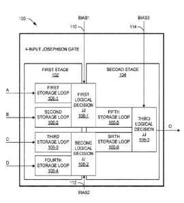
[0007] FIG. 1 is a block diagram of an example four-input Josephson gate.
[0008] FIG. 2A is a circuit diagram of an example four-input AND gate, the
logical
function of which is shown symbolically in FIG. 2B.
[00091 FIG. 3A is a circuit diagram of an example four-input OR gate, the
logical
function of which is shown symbolically in F.G. 3B.
[0010] FIG. 4A is a circuit diagram of an example four-input AND-OR gate,
the logical
function of which is shown symbolically in FIG. 4B.
[0011] FIG. 5A is a circuit diagram of an example four-input OR-AND gate,
the logical
function of which is shown symbolically in FIG. 5B.
[0012] FIGS. 6A and 6B are flow diagrams of example methods of determining
a logical
output from a four-input RQL gate based on SFQ pulse inputs.
[0013] FIG. 7 is a flow diagram of an example method of determining a
logical AND
value based on SFQ pulse inputs.
[0014] FIG. 8 is a flow diagram of an example method of determining a
logical OR value
based on SFQ pulse inputs.
[0015] FIG. 9 is a flow diagram of an example method of determining a
logical AND-OR
value based on SFQ pulse inputs.
[0016] FIG. 10 is a flow diagram of an example method of determining a
logical
OR-AND value based on SFQ pulse inputs.
3
CA 03088259 2020-07-10
WO 2019/152282 PCT1US2019/015233
DETAILED DESCRIPTION
[0017] This disclosure relates generally to logical gate circuits useful,
for example, in
reciprocal quantum logic (RQL) systems, and related methods. This disclosure
more specifically
relates to such gates having four inputs, including AND gates, OR gates, AND-
OR (A022)
gates. and OR-AND (0A22) gates. The disclosure more specifically provides a
family of four-
input logic gates that each utilize a distributed decision Josephson junction
and cascadable RQL
logic functions.
[0018] FIG. 1 shows a four-input Josephson gate 100 having four logical
inputs A, B, C,
D, and output 0. Gate 100 includes first stage 102, configured to receive
inputs A, B, C, D,
which can consist of positive or negative single flux quantum (SFQ) pulses
corresponding to
asserted or de-asserted logic states, respectively. Gate 100 further includes
second stage 104,
configured to provide output 0, which also can consist of positive or negative
SFQ pulses
corresponding to asserted or de-asserted logic states, respectively. Each
logical input A, B, C, D
has associated with it at least one storage loop among storage loops 106-1
through 106-4.
Although first stage 102 is illustrated as having one storage loop per input,
each input can have
more than one storage loop associated with it.
[0019] First logical decision Josephson junction (JJ) 108-1 is common to
(i.e., shared by)
first and second input storage loops 106-1, 106-2, and triggers based on
inputs A, B. Second
logical decision JJ 108-2 is common to (i.e., shared by) third and fourth
input storage
loops 106-3, 106-4, and triggers based on inputs C, D. Second stage 104
includes fifth and sixth
storage loops 106-5, 106-6. Fifth storage loop 106-5 is made up of first
logical decision JJ 108-1
as well as third logical decision JJ 108-3. Sixth storage loop 106-6 is made
up of second logical
decision JJ 108-2 as well as third logical decision JJ 108-3. Third logical
decision JJ 108-3 is
common to (i.e., shared by) fifth and sixth storage loops 106-5, 106-6, and
triggers based on the
triggering of either or both of first and second logical decision JJs 108-1,
108-2.
[0020] The assertion or de-assertion of output 0 of four-input gate 100 can
be based on
the triggering of third logical decision JJ 108-3. Depending on the
configuration of gate 100, the
assertion or de-assertion of output 0 can be based on any, some, or all of
inputs A, B, C, D. For
4
CA 03088259 2020-07-10
WO 2019/152282 PCT1US2019/015233
example, output 0 can propagate a positive SFQ pulse corresponding to an
asserted output logic
state and a negative SFQ pulse corresponding to a de-asserted output logic
state. As examples,
four-input gate 100 can be configured as an AND gate, an OR gate, an OR-AND
gate, or an
AND-OR gate. Second stage 104 can include an output Josephson transmission
line (JTL) (not
shown in FIG. 1) to amplify the output of third logical decision JJ 108-3.
[0021] The triggering of first logical decision LI 108-1 can be based not
only on
inputs A, B, but also on a first bias signal BIAS1 provided to first logical
decision JJ 108-1 via
first bias line 110. Similarly, the triggering of second logical decision JJ
108-2 can be based not
only on inputs C, D, but also on a second bias signal BIAS2 provided to second
logical decision
JJ 108-2 via second bias line 112. Likewise, the triggering of third logical
decision JJ 108-3 can
be based not only on the states of first logical decision JJ 108-1 and second
logical decision
JJ 108-2, but also on a third bias signal provided to third logical decision
JJ 108-3 via third bias
line 114. Bias signals BIAS1, BIAS2, BIAS3 provided on bias lines 110, 112,
114 can provide
both AC and DC bias. Thus, for example, bias signals provided on lines 110,
112, 114 can act as
clocks to Josephson gate 100, causing the evaluation of the inputs A, B, C, D
to produce the
output 0 at certain points in time according to the AC components of bias
signals BIAS1,
B1AS2, BIAS3. In some examples, first and second bias signals provided on
lines 110, 112 can
have the same AC phase while third bias signal provided on line 114 can have
an AC phase that
is different from the AC phase of the first and second bias signals, e.g., 180
out of phase with
the first and second bias signals.
[0022] FIG. 2A illustrates a four-input AND RQL gate that performs a
logical function
illustrated symbolically in FIG. 2B, showing a single four-input AND gate.
First stage 202 can
correspond to first stage 102 in FIG. 1 and second stage 204 can correspond to
second stage 104
in FIG. I. In first stage 202, each input ai, hi, ci, di is provided via a
respective one of leading
inductors Lina_0, Linb_0, Linc_0, Lind_0. These leading inductors each allow a
corresponding
input to be connected to a driving JTL or to the output of another gate.
[0023] First stage 202 has two JTL input branches corresponding to inputs
ai, bi that join
at first dovetail node 206. Together with first logical decision JJ b0_0,
these two input branches
CA 03088259 2020-07-10
WO 2019/152282 PCT1US2019/015233
form storage loops to separately receive and store inputs ai, bi until a first
logical decision can be
made, i.e., until a first logic condition is met. A first storage loop
corresponding to input ai is
made up of first input JJ b2a_0, first storage inductor FLstora_0, and first
logical decision JJ
b0_0. A second storage loop corresponding to input bi is made up of second
input JJ b2b_0,
second storage inductor FLstorb_0, and first logical decision JJ b0_0. Thus,
first logical decision
JJ b0_0 is common to both the first and second storage loops.
[0024] First stage 202 further has two more JTL input branches
corresponding to inputs
ci, di that join at second dovetail node 208. Together with second logical
decision JJ b0_1, these
two input branches form storage loops to separately receive and store inputs
ci, di until a second
logical decision can be made, i.e., until a second logic condition is met. A
third storage loop
corresponding to input ci is made up of third input JJ b2c_0, third storage
inductor FLstorc_0,
and second logical decision JJ b0_1. A fourth storage loop corresponding to
input di is made up
of fourth input JJ b2d_0, fourth storage inductor FLstord_0, and second
logical decision JJ b0_1.
Thus, second logical decision JJ b0_1 is common to both the third and fourth
storage loops. First
stage 202 narrows from four input branches to two intermediate branches.
100251 Second stage 204 combines the outputs of these two intermediate
branches to
further narrow to a single output branch at dovetail node 210. Together with
third logical
decision JJ bl_0, the two intermediate branches form fifth and sixth storage
loops to separately
receive and store the two intermediate outputs of the first stage 202 until a
third logical decision
can be made, i.e., until a third logic condition is met. A fifth storage loop
storing the
intermediate result of the first logic decision made with regard to inputs ai,
bi is made up of first
logical decision JJ b0_0, fifth storage inductor L4_0, and third logical
decision JJ bl_0. A sixth
storage loop storing the intermediate result of the second logic decision made
with regard to
inputs ci, di is made up of second logical decision JJ b0_1, sixth storage
inductor L4_1, and third
logical decision JJ b1_0. Thus, first logical decision JJ b0_0 is common to
all three of the first,
second, and fifth storage loops, second logical decision JJ b0_1 is common to
all three of the
third, fourth, and sixth storage loops, and third logical decision JJ bl_O is
common to both of the
fifth and sixth storage loops.
6
CA 03088259 2020-07-10
WO 2019/152282 PCT1US2019/015233
[0026] In gate circuit 200, first AC and DC bias input bias! is provided to
first logical
decision JJ b0.._0 via first bias inductor LOA second AC and DC bias input
bias2 is provided to
second logical decision JJ b0_1 via second bias inductor L0_1, and third AC
and DC bias input
bias3 is provided to third logical decision JJ bl_O via third bias inductor
L1_0. Output ao may
also be connected to a JTL or to the input of another gate, for example, to
propagate a positive
output pulse representing the assertion of gate 200 to logical "high." A
subsequent negative
output pulse propagated from output ao can then represent the de-assertion of
gate 200 to logical
"low."
[0027] The selections of component sizes in each storage loop provide a
unidirectional
data flow, i.e., from left to right of the circuit 200 as illustrated in FIG.
2A. Circuit 200 operates
on SFQ pulses, which each place one (I)o (about 2.07 mA pH) of current into a
storage loop. The
magnitude of current through such a storage loop is determined by the size of
the storage
inductor in the storage loop. Thus, for each input, the inductance value of
the leading inductor
(e.g., Lina_0) can be small (e.g., between about 8 pH and 9 pH, e.g., 8.5 pH)
in comparison to
the inductance value of the storage inductor (e.g., FLstora_0). On the other
hand, the storage
inductor can be sized to be relatively large (e.g., between about 30 pH and 40
pH, e.g., 35 pH)
(e.g., about four times larger than the corresponding leading inductor) to
reduce the magnitude of
the stored current induced by an input SFQ pulse. In some examples, the
magnitude of a current
introduced at an input (e.g., ai) is about four times larger than the current
stored in a storage loop.
The input Li for input ai, b2a_0, is also sized such that the driving JTL is
capable of triggering
this JJ to put current into the corresponding storage loop, but the current in
the storage loop is
never sufficient to untrigger input JJ b2a_0 and allow the stored pulse to
back out of the input.
The storage loops associated with inputs bi, ci, and di can have the same
structure as the storage
loop for input ai, and thus can have the same unidirectional flow properties.
[0028] The logical decision Hs b0_0, b0_1, bl_O perform the logic function
of the
gate 200. The combination of any two inputs, plus the bias bias_1, bias2, or
bias3, is sufficient
to switch the corresponding logical decision JJ b0_0, b0_1, or bl_O in either
direction. An AC
component (e.g., a sine wave component) of any of bias signals biasl, bias2,
bias3 in gate 200 of
7
CA 03088259 2020-07-10
WO 2019/152282 PCT1US2019/015233
FIG. 2A can act as a clock signal to gate 2()0, which can evaluate the logical
inputs twice per
cycle of the clock signal. The AC phase of each bias signal can have
alternating positive and
negative portions. During the positive portion of the AC phase, the
corresponding logical
decision JJ evaluates its connected inputs to decide whether its output should
be asserted; during
the negative portion of the AC phase, the corresponding logical decision JJ
evaluates inputs to
decide whether its output should be de-asserted. Thus, output ao is only ever
asserted on the
positive portion of the AC phase of bias signal bias3 and is only ever de-
asserted on the negative
portion of the AC phase of bias signal bias3.
[0029] Each logical decision JJ b0_0, b0_1, bl_O in gate circuit 200
performs a majority
function on the basis of two logical inputs and a third pseudo-input tied to a
low voltage rail
(e.g., ground) that functions as an immutable logical "0." First logical
decision JJ b0_0 triggers,
on the positive phase portion of bias signal bias I, when a majority two out
of three of its inputs
have been asserted, those inputs consisting of ai, bi, and the permanent "0"
from third branch
consisting of inductor FLgnda_0. Because a two-of-three majority is required
for assertion and
one "input" is always "0," first logical decision JJ b0_0 only triggers when
both ai and bi have
been asserted. First logical decision JJ b0_0 untriggers, on the negative
phase portion of bias
signal bias I, when less than a majority two out of three of its inputs have
been asserted. Thus,
first logical decision JJ b0_0 untriggers when either ai or bi have been de-
asserted. Second
logical decision JJ b0_1 functions similarly based on its logical inputs ci,
di, and its bias signal
bias2. Third logical decision II bl_O functions similarly based on the outputs
of first and second
logical decision LIS b0_0, b0_1 and bias signal bias3. Accordingly, the
correct four-input AND
logical functionality is produced at output ao.
[0030] Inductor FLgnda_O can be somewhat larger than the other storage
inductors
FLstora_0, FLstorb_O to compensate for the eliminated parasitic input
inductance that results
from having no input JJ associated with that branch. For example, in gate 200,
the inductance
value of inductor FLgnda_O can be between about 32 pH and 42 pH, e.g., 36 pH.
[0031] The sequence of events in gate circuit 200 that occur when a single
input is
asserted will now be described. An input pulse, e.g., a single flux quantum
(SFQ) pulse, arrives
8
CA 03088259 2020-07-10
WO 2019/152282 PCT1US2019/015233
at input ai. This induces superconducting current through leading inductor
Lina_O and input JJ
b2a_0. This current in turn triggers input JJ b2a_0, raising its
superconducting phase from 0
to 27t. The triggering of input JJ b2a_0 induces an equal and opposite current
(e.g., one (Do worth
of current) in leading inductor Lina_0, annihilating the initial input
current, and also induces a
superconducting current in the first storage loop formed by input JJ b2a_0,
first storage inductor
FLstora_0, and first logical decision JJ b0_0. 'This first storage loop
current alone is insufficient
to trigger logical decision JJ b0_0, and will remain trapped indefinitely in
the first storage loop if
no further inputs are applied. A negative input pulse arriving at input ai
would reverse the
above-described effects, annihilating the positive current stored in the first
storage loop with an
equal and opposite current, thus returning the circuit to its initial state.
Logical inputs hi, ci, and
di opel ate in the same manner.
[0032] A positive current stored in the first storage loop is, by itself,
insufficient to
trigger logical decision JJ b0_0, even with the AC and DC bias bias 1. not
only because logical
decision JJ b0_0 may be a larger JJ than the Ths preceding it in circuit 200,
but also because of
the majority structure of circuit 200. The additional load presented to
logical decision JJ b0_0 by
the components associated with unasserted logical inputs bi and grounded
pseudo-input through
FLgnda_O inhibits logical decision JJ b0_0 from triggering. Thus, assertion of
a majority of
inputs is required to cause b0_0 to trigger.
[0033] When logical input bi is asserted following the assertion of logical
input ai, e.g.,
by introducing another positive SFQ pulse to the bi input, another positive
current is made to
circulate in the second storage loop formed by input JJ b2b_0, second storage
inductor
FLstorb_0, and first logical decision JJ b0_0. Then, both of input J.Is b2a_0
and b2b_0 are in
the 2x state. Both loop currents, induced by respective positive input pulses,
will persist in their
respective storage loops until a subsequent negative pulse on the respective
input removes the
corresponding loop current, or until the clocking function of the AC component
of bias signal
biasl triggers logical decision JJ b0_0 to transform the inputs into an
output. Because of this
storage functionality, inputs needed to amount to a majority number of input
assertions need not
arrive within the same clock cycle.
9
CA 03088259 2020-07-10
WO 2019/152282 PCT1US2019/015233
[00341 Both of these input loop currents bias first logical decision JJ
b0_0 towards a
positive transition, but due to the size of input loop storage inductors
FLstora...0 and FLstorb_0,
these currents are insufficient to cause this transition without additional
bias current provided by
the AC and DC bias signal bias I. When the AC component of this bias signal
has reached
sufficient positive magnitude, i.e., when first logical decision JJ b0_0 is
positively "clocked,"
first logical decision JJ b0_0 triggers. The stored positive currents in the
first and second storage
inductors FLstora_0, FLstorb_O are annihilated by resultant equal and opposite
currents.
Additionally, a positive current is placed into fifth storage loop via fifth
storage inductor L4_0
and third logical decision JJ bl_0.
[0035] Second logical decision JJ b0_1 functions similarly to place a
positive current into
sixth storage loop via sixth storage inductor L4_1 and third logical decision
JJ bl_O based on
assertions of logical inputs ci and di and the positive clocking function of
second bias signal
bias2. The stored currents in the fifth and sixth storage loops, in
combination with the AC
component of bias signal bias3, trigger third logical decision JJ bl_0,
sending a positive SFQ
pulse out of output ao, asserting the output and providing the correct four-
input logical AND
function for gate 200. As well, this triggering of third logical decision JJ
bl_O annihilates the
stored positive currents in inductors L4_0 and L4_1.
[0036] A single negative pulse arriving at any of the initially asserted
inputs ai, bi, ci, or
di will provide a negatively biasing current in a corresponding storage loop,
such that in
combination with the respective AC and DC biases they will unfli.p
corresponding first or second
logical decision Es b0_0 or b0_1 by causing such JJ to transition out of its a
phase. This de-
assertion propagates through to a similar de-assertion of third logical
decision JJ bl_0, thereby
de-asserting the output ao of gate 200 back to logical "low." This will occur
when the AC
component of bias signal bias3 has reached sufficient negative magnitude.
[0037] Gate 200 shows the case where grounding one of three inputs of a two-
of-three
majority structure (effectively tying this third input, or pseudo-input, to
logical "low") creates a
two-input AND structure with the two remaining inputs (the logical inputs),
and two such
majority structures can be tied together, at third dovetail node 210, with a
third grounded
CA 03088259 2020-07-10
WO 2019/152282 PCT1US2019/015233
pseudo-input (via inductor FLgndc_O in circuit 200) to result, ultimately, in
a four-input AN.D
gate. Using a DC bias to induce one (1)0 (i.e., one SFQ pulse) of current on
one of the
pseudo-inputs (effectively tying it to logical "high") in the three-input
majority structure, instead
of grounding one of the pseudo-inputs as in circuit 200, creates a two-input
OR structure from
the remaining two logical inputs. A four-input OR gate 300, as shown in FIG.
3A, can be
constructed accordingly, with the appropriate modification of the four-input
AND gate 200 of
FIG. 2A.
[0038] Following from the above description, FIG. 3A shows example four-
input OR
gate 300, in which output oo is asserted if any one or more of inputs ai, bi,
ci, or di are asserted.
Thus, gate 300 performs a logical function illustrated symbolically in FIG.
3B, showing a single
four-input OR gate. In the illustrated configuration, whereas circuit 200 ties
pseudo-input
branches to a circuit ground, circuit 300 introduces bias quantizing JJs
b2DCa_0, b2DCb_0,
bODC_O between transformer-coupled input inductors DC_c_0, DC_c_1, DC_c_2 and
substitute
storage inductors FLstorDCa_0, FLstorDCb_0, and L4DC_0, respectively.
Transformer-coupled
input inductors1DC_c_0, DC_c_1. DC_c_2 are transformer-coupled to respective
DC flux bias
lines 312, 314, 316. Bias quantizing JJs b2DCa_0, b2DCb_0, bODC_O each
quantize the DC
bias current supplied through transformer-coupled input inductors DC_c_0,
DC_c_1, DC_c_2,
respectively, and improve operating margins.
[0039] Thus, each logical decision JJ b0_0, b01, bl_O in four-input OR
gate 300
effectively considers, in addition to the states of two respective logical
inputs, a third input,
referred to herein as a pseudo-input, that biases its respective logical
decision JJ toward
triggering and thereby presents an immutable logical "1," effectively
transforming the majority
function of each of the three "three"-input structures into a two-input OR
structure. This differs
from four-input AND gate 200 in which each logical decision JJ b0_0, b01, bl_O
effectively
considers, in addition to the states of two respective logical inputs, a third
input, or pseudo-input,
that biases its respective logical decision JJ against triggering and thereby
presents an immutable
logical "0," effectively transforming the majority function of each of the
three "three"-input
structures of gate 200 into a two-input AND structure.
11
CA 03088259 2020-07-10
WO 2019/152282 PCT1US2019/015233
[0040] The pseudo-inputs illustrated in FIG. 3A function as follows. DC
current
provided through any of DC flux bias lines 312, 314, 316 stays constant
throughout system
operation. At system start-up, the DC current through DC flux bias lines 312.
314, 316 couple
current into input inductors DC_c_0, DC_c_1, DC_c_2 to which they are
transformer-coupled,
via the AC transient that occurs at system power-up. This triggers bias
quantizing Ms b2DCa_0,
b2DCb_0, bODC_O once at the beginning of operation, putting a positive current
into each of
substitute storage inductors FLstorDCa_0, FLstorDCb_0, and L4DC_0.
[0041] Any or all of the pseudo-inputs used to present an immutable logical
"high"
illustrated in gate circuits 300, 400, or 500 of FIGS. 3A, 4A, or 5A could be
realized differently
than as shown in FIG. 3A. As one example, the quantizing JJ (e.g., b2DCa_0,
b2DCb_0,
bODC_O) and the separate substitute storage inductor (e.g., FLstorDCa_0,
FLstorDCb_0,
L4DC_0) could be omitted such that DC flux is transformer-coupled into an
inductor in the
pseudo-input branch (e.g., DC_c_0, DC_c_1, DC_c_2) and that inductor serves as
the substitute
storage inductor in the pseudo-input branch. Thus, the pseudo-input in any or
each majority
structure can be initialized with application of one 00 of current directly
via the transformer
coupling to the DC current. As another example, in any logical "high" pseudo-
input instance, an
inductor transformer-coupled to a DC flux bias line can placed in parallel
with a quantizing JJ,
both of which can be configured in series with the substitute storage inductor
(e.g.,
FLstorDCa_0, FLstorDCb_0, L4DC_0) so as to provide the aforementioned
initializing current.
Thus, the "high" pseudo-input in any or each majority structure can be
initialized with
application of one (Do of current indirectly, via the transformer and
quantizing JJ. The
initialization can also be performed by any other suitable mechanism.
[0042] The circuit 300 having been so initialized, first logical decision
JJ b0_0 in OR
gate 300 of FIG. 3A then effectively sees "one" out of "three" inputs
asserted, the "one" asseited
input being the non-logical, pseudo-input initiated by the DC bias on flux
bias line 312, and
triggers in response to at least one asserted input among logical inputs ai or
bi (and the clocking
function of bias!). Upon such triggering, the positive current in first
substitute storage inductor
FLstorDCa_0 is annihilated, b2DCa_0 does not untrigger, positive currents in
storage inductors
12
CA 03088259 2020-07-10
WO 2019/152282 PCT1US2019/015233
FLstora_O or FLstorb_O are annihilated should the inputs associated with those
storage inductors
have been asserted, negative currents are induced in the storage inductors
associated with any
unasserted input among ai or bi, and a positive current is placed into the
fifth storage loop
formed by first logical decision JJ b0_0, fifth storage inductor L4_0, and
third logical decision JJ
bl_0.
[0043] Thereafter, if negative pulses are applied to de-assert all of
previously asserted
inputs among logical inputs ai or bi, the negative currents stored in the
storage loops associated
with the ai, bi logical inputs combine to bias first logical decision JJ b0_0
to untrigger upon the
next negative portion of the AC component of the bias signal bias 1, which in
turn propagates a
negative pulse into the fifth storage loop comprising fifth storage inductor
L4_0. This
untriggering of first logical decision JJ b0_0 restores the positive current
to substitute storage
inductor FLstorDCa_0, bringing the upper-left portion of circuit 300 back to
its initial state, i.e.,
the state following start-up injection of initial positive current into
substitute storage inductor
FLstorDCa_O via DC flux bias line 312.
[0044] Similarly, after system-start-up, second logical decision JJ b0_1.
in OR gate 3(X) of
FIG. 3A effectively sees "one" out of "three" inputs asserted, the "one"
asserted input being the
non-logical, pseudo-input initiated by the DC bias on flux bias line 314, and
triggers in response
to at least one asserted input among logical inputs ci or di (and the clocking
function of bias2).
Upon such triggering, the positive current in second substitute storage
inductor FLstorDCb_O is
destroyed, b2DCb_0 does not untrigger, positive currents in storage inductors
FLstorc_O or
FLstord_O are destroyed should the inputs associated with those storage
inductors have been
asserted, negative currents are induced in the storage inductors associated
with any unasserted
input among ci or di, and a positive current is placed into the sixth storage
loop formed by
second logical decision JJ b0_1, sixth storage inductor L4_1, and third
logical decision JJ bl_0.
[0045] Thereafter, if negative pulses are applied to de-assert all of
previously asserted
inputs among logical inputs ci or di, the negative currents stored in the
storage loops associated
with the cd, di logical inputs combine to bias second logical decision JJ b0_1
to untrigger upon
the next negative portion of the AC component of the bias signal bias2, which
in turn propagates
13
CA 03088259 2020-07-10
WO 2019/152282 PCT1US2019/015233
a negative pulse into the sixth storage loop comprising sixth storage inductor
L4_1. This
untriggering of second logical decision JJ b0_1 restores the positive current
to substitute storage
inductor FLstorDCb_0, bringing the lower-left portion of circuit 300 back to
its initial state, i.e.,
the state following stait-up injection of initial positive current into
substitute storage inductor
FLstorDCb_O via DC flux bias line 314.
[0046] The triggering and untriggering of third logical decision JJ bl_O in
OR gate
circuit 300 works similarly to as described above with first and second
logical decision Ds b0_0
and b0_1. After system start-up and injection of a current into third
substitute storage inductor
L4DC_0, the majority structure associated with third logical decision JJ bl_O
sees "one" of
"three" inputs asserted and therefore only requires one the remaining inputs
associated with first
or second logical decision Hs b0_0 or b0_1 to be asserted in order to have a
majority "two" of
"three" assertions and thus to cause the triggering of third logical decision
JJ bl_O (in
conjunction with the clocking function of bias3) and send an SFQ pulse out of
output oo to assert
it. De-assertion also works substantially as described above, when both first
or second logical
decision Bs b0_0 and b0_1 are de-asserted (again in conjunction with the
clocking function of
bias3). The correct logical function of a four-input OR gate is thereby
achieved in circuit 300.
[0047] FIG. 4A shows an example four-input AND-OR (AO) gate 400,
specifically, an
A022 gate, constructed based on the previously described topologies, to
produce the
functionality symbolically shown in FIG. 4B. Conceptually, A022 gate 400 is an
OR gate
having its inputs provided by the outputs of AND gates. Accordingly, the first
stage of A022
gate 400 is identical to the first stage 202 of gate 200 (providing AND
functionality) whereas the
second stage of A022 gate 400 is identical to the second stage of gate 300
(providing OR
functionality). These stages operate substantially as previously described in
this disclosure, with
the triggering of first-stage logical decision .11s bO_0, b0_1 being
influenced not only by logical
inputs ai, bi and ci, di, respectively, but also by immutable "0" pseudo-
inputs provided through
inductors FLgnda_O and FLgndb_0, respectively, and with the triggering of
second-stage logical
decision JJ bl_O being influenced not only by the outputs of the first-stage
logical decision J.Js,
but also by the immutable "1" pseudo-input provided through inductor L4DC_0.
A022 gate 400
14
CA 03088259 2020-07-10
WO 2019/152282 PCT1US2019/015233
further includes an additional JTL component at its output consisting of
inductor L5_0, JJ b2_0,
and bias signal bias4 provided via inductor L2_0. to provide additional
amplification.
[0048] Conversely, FIG. 5A shows an example four-input OR-AND (OA) gate,
specifically, an 0A22 gate, constructed based on the previously described
topologies, to produce
the functionality symbolically shown in FIG. 5B. Conceptually, 0A22 gate 500
is an AND gate
having its inputs provided by the outputs of OR gates. An 0A22 gate thus
provides an asserted
output only when all of the inputs to its conceptual AND stage are asserted,
in turn requiring that
that at least one of the inputs to each of its conceptual OR stages is
asserted. Accordingly, the
first stage of 0A22 gate 500 is identical to the first stage of gate 300
(providing OR
functionality) whereas the second stage of 0A22 gate 500 is identical to the
second stage 204 of
gate 200 (providing AND functionality). These stages operate substantially as
previously
described in this disclosure, with the triggering of first-stage logical
decision JJs b0_0, b0_1
being influenced not only by logical inputs ai, bi and ci, di, respectively,
but also by
immutable "1" pseudo-inputs provided through inductors FLstorDCa_O and
FLstorDCb_0,
respectively, and with the triggering of second-stage logical decision JJ b
1_0 being influenced
not only by the outputs of the first-stage logical decision JJs, but also by
the immutable "0"
pseudo-input provided through inductor FLgndc_0. 0A22 gate 500 further
includes an
additional JTL component at its output consisting of inductor L5_0, JJ b2_0,
and bias signal
bias4 provided via inductor L2_0, to provide additional amplification.
[0049] Each of the four-input gate designs 2(X), 3(X), 4(X). 500 consist of
an amalgamation
of essentially three two-input gates, using Boolean logic, to create larger
gates, leveraging the
logical equivalences of (AB)(CD) = ABCD in gate 200 as well as (A+B)+(C+D) =
A+B+C+D in
gate 300. Using the input and logical decision JJs of two two-input AND gates
and combining
them with the decision and driving portions of another AND gate, a four-input
AND gate 2(X) is
realimd in FIG. 2A. A four-input OR gate 300 is realized similarly in FIG. 3A.
In a similar
fashion, by using the input and decision JJs of two two-input AND gates, and
attaching them to
the decision and driving portions of a two-input OR gate, the AND-OR gate
structure 400 of
FIG. 4A can be achieved, and by using two two-input OR gate front-ends and the
back-end of an
CA 03088259 2020-07-10
WO 2019/152282
PCT1US2019/015233
AND gate, the OR-AND gate structure 500 of FIG. 5A can be created. Prior to
the invention of
the gates in the present disclosure, the state of the art required using three
independent two-input
gates, as well as a Josephson transmission line in between the two two-input
gates and the last
two-input gate. The new four-input gates described herein make layouts
smaller, and the gates
themselves are faster than their multiple-gate counterparts. The new four-
input gates reduce chip
area of circuitry in RQL digital logic, which in turn reduces chip cost by
allowing more circuits
to be placed on chips. As a by-product, the circuits are also faster.
[0050] FIG. 6A
shows method 600 of determining a logical output from an RQL gate
having four logical inputs based on SFQ pulse inputs. Positive SFQ pulses are
provided 602 to
assert one or more logical inputs of an RQL gate having four logical inputs to
place 604 one or
more currents in one or more logical input storage loops associated with the
asserted inputs, e.g.,
one loop per input, where the gate has four such logical input storage loops.
The RQL gate can
be, for example, like any of gates 100, 200, 300, 400, or 500 shown in FIGS. 1-
5, or can be
extensions of such examples. A logical decision JJ that is configured to
trigger based on the
assertion of a certain number or certain ones of the logical inputs then
triggers 606. The JJ can
be configured to trigger when at least one of two logical input storage loops
have received
positive SFQ pulses, thereby providing an OR function, or only when both of
the two logical
input storage loops have received positive SFQ pulses, thereby providing an
AND logic function.
The JJ can be so configured, for example, by making it common to two of the
logical input
storage loops in the RQL gate, by effectively tying to logical "high" or
logical "low" additional
inputs not counted among the logical inputs, by providing appropriate biasing,
and/or by
appropriate component sizing. A cascaded logical decision JJ, "downstream" of
the previously
triggered 606 JJ in the RQL gate in terms of logic flow, then triggers 608. An
assertion signal,
generated as a result of the triggering 608 of the cascaded logical decision
JJ, then
propagates 610 from an output of the RQL gate. The assertion signal can be,
for example, a
single SFQ pulse.
[0051] FIG. 6B
shows method 650 of determining a logical output from an RQL gate
having four logical inputs based on SFQ pulse inputs, which can continue from
method 600
16
CA 03088259 2020-07-10
WO 2019/152282
PCT1US2019/015233
shown in FIG. 6A. Negative SFQ pulses are provided 612 to de-assert one or
more logical
inputs of an RQL gate having four logical inputs to place 614 one or more
currents in one or
more logical input storage loops associated with the asserted inputs, e.g.,
one loop per input,
where the gate has four such logical input storage loops. The placed currents
can be negative
currents, i.e., currents equal and opposite to the currents placed 604 in
method 600. Again, the
RQL gate can be, for example, like any of gates 100, 200, 300, 400, or 500,
shown in FIGS. 1-5,
or can be extensions of such examples. A logical decision JJ that is
configured to untigger
based on the de-assertion of a certain number or certain ones of the logical
inputs then
untriggers 616. The JJ can be configured to trigger when at least one of two
logical input storage
loops associated with previously asserted logical inputs have received
negative SFQ pulses,
thereby providing an AND function, or only when both of two logical input
storage loops
associated with previously asserted logical inputs have received negative SFQ
pulses, thereby
providing an OR logic function. The JJ can be so configured, for example, by
making it
common to two of the logical input storage loops, by effectively tying to
logical "high" or logical
"low" additional inputs not counted among the logical inputs, by providing
appropriate biasing,
and/or by appropriate component sizing. A cascaded logical decision JJ,
"downstream" of the
previously untriggered 616 JJ in the RQL gate in terms of logic flow, then
untriggers 618. A de-
assertion signal, generated as a result of the untriggering 618 of the
cascaded logical decision JJ,
then propagates 620 from an output of the RQL gate. The assertion signal can
be, for example, a
single SFQ pulse, e.g., a single negative SFQ pulse, opposite in direction to
the pulse
propagated 610 in method 600.
[00521 FIG. 7
illustrates an example method 700 of determining a logical AND value
based on four SFQ pulse inputs. Positive SFQ pulses are provided 702 to assert
all of the logical
inputs of an RQL AND gate having four logical inputs to place 704 currents in
all four logical
input storage loops associated with the asserted inputs, i.e., one loop per
input. The RQL AND
gate can be, for example, like gate 200 shown in FIG. 2A, or can be extensions
of such example
providing a greater number of inputs. First and second logical decision JJs
trigger 706 based on
the placement of currents 704. The first and second logical decision Bs can
each be configured
17
CA 03088259 2020-07-10
WO 2019/152282 PCT1US2019/015233
to trigger 706 based on the assertion of two of the logical inputs. The JJs
can be so configured,
for example, by making each of them common to both of the logical input
storage loops
associated with said inputs, by effectively tying to logical "low" an
additional input to each JJ
not counted among the logical inputs, by providing appropriate biasing, and/or
by appropriate
component sizing. A cascaded logical decision JJ, "downstream" of the
previously triggered 706
J.ls in the RQL gate in terms of logic flow, then triggers 708 based on the
prior triggerings 706.
An assertion signal, generated as a result of the triggering 708 of the
cascaded logical decision
JJ, then propagates 710 from an output of the RQL AND gate. The assertion
signal can be, for
example, a single SFQ pulse.
[0053] FIG. 8 illustrates an example method 800 of determining a logical OR
value based
on SFQ pulse inputs. One or more positive SFQ pulses are provided 802 to
assert any or all of
the logical inputs of an RQL OR gate having four logical inputs to place 804
currents in one or
more input storage loops associated with the asserted inputs, i.e., one loop
per input. The RQL
OR gate can be, for example, like gate 300 shown in FIG. 3A, or can be
extensions of such
example. A logical decision JJ triggers 806 based on the placement of the
current(s) 804. The
logical decision JJ can be configured to trigger 806 based on the assertion of
at least one of two
logical inputs. The JJ can be so configured, for example, by making it common
to both of the
logical input storage loops associated with said inputs, by effectively tying
to logical "high" an
additional input to the JJ not counted among the logical inputs, by providing
appropriate biasing,
and/or by appropriate component sizing. A cascaded logical decision JJ,
"downstream" of the
previously triggered 806 .1.1 in the RQL gate in terms of logic flow, then
triggers 808 based on the
prior triggering 806. An assertion signal, generated as a result of the
triggering 808 of the
cascaded logical decision JJ, then propagates 810 from an output of the RQL OR
gate. The
assertion signal can be, for example, a single SFQ pulse.
[0054] FIG. 9 illustrates an example method 900 of determining a logical
A022 value
based on at least two SFQ pulse inputs. At least two positive SFQ pulses are
provided 902 to
assert at least two paired logical inputs of an RQL A022 gate having four
logical inputs arranged
as two pairs of two logical inputs, thereby placing 904 currents at least two
logical input storage
18
CA 03088259 2020-07-10
WO 2019/152282 PCT1US2019/015233
loops associated with the asserted paired inputs, i.e., one loop per input.
The RQL A022 gate
can be, for example, like gate 400 shown in FIG. 4A, or can be extensions of
such example. A
logical decision JJ triggers 906 based on the placement of the currents 904.
The logical decision
JJ can be configured to trigger 906 based on the assertion of both of the
associated logical inputs.
The JJ can be so configured, for example, by making it common to both of the
logical input
storage loops associated with said inputs, by effectively tying to logical
"low" an additional input
to the JJ not counted among the logical inputs, by providing appropriate
biasing, and/or by
appropriate component sizing. A cascaded logical decision JJ, "downstream" of
the previously
triggered 906 JJ in the RQL gate in terms of logic flow, then triggers 908
based on the prior
triggering 906. An assertion signal, generated as a result of the triggering
908 of the cascaded
logical decision JJ, then propagates 910 from an output of the RQL A022 gate.
The assertion
signal can be, for example, a single SFQ pulse.
[0055] FIG. 10 illustrates an example method 10(X) of determining a
logical 0A22 value
based on at least two SFQ pulse inputs. At least two positive SFQ pulses are
provided 1002 to
assert at least two unpaired logical inputs of an RQL 0A22 gate having four
logical inputs
arranged as two pairs of two logical inputs, thereby placing 1004 currents in
at least two logical
input storage loops associated with the asserted unpaired inputs, i.e., one
loop per input. The
RQL 0A22 gate can be, for example, like gate 500 shown in FIG. 5A, or can be
extensions of
such example. First and second logical decision JJs trigger 1006 based on the
placement 1004 of
currents. The first and second logical decision us can each be configured to
trigger 1006 based
on the assertion of at least one associated logical input. Each JJ can be so
configured, for
example, by making it common to two associated logical input storage loops, by
effectively tying
to logical "high" an additional input not counted among the logical inputs, by
providing
appropriate biasing, and/or by appropriate component sizing. A cascaded
logical decision JJ,
"downstream" of the previously triggered 1006 Ths in the RQL gate in terms of
logic flow, then
triggers 1008 based on the prior triggerings 1006. An assertion signal,
generated as a result of
the triggering 1008 of the cascaded logical decision JJ, then propagates 1010
from an output of
the RQL 0A22 gate. The assertion signal can be, for example, a single SFQ
pulse.
19
CA 03088259 2020-07-10
WO 2019/152282 PCT1US2019/015233
[0056] The four-input gates 200, 300. 400, 500 described herein are
examples. but do not
include all possible configurations. As shown by these examples, each stage
may separately be
configured to perform and AND, OR, or majority function. All combinations of
these functions
may be realized including all four-input combinations of AND arid OR. If any
stages arc
configured to perform a majority function, additional inputs can be added as
the pseudo-inputs of
the AND and OR gates become real primary inputs. The use of logic gates with
four or more
inputs, including the examples disclosed herein, can improve the efficiency
and density of RQL
logic. Gates that can implement larger logic functions allow reduced die sizes
and, by extension,
reduced cost per die. The logic gates described herein can operate according
to RQL data
encoding, where, for example, it would be impermissible for a logic gate to
propagate two
positive output pulses in a row or two negative output pulses in a row.
[0057] What have been described above are examples of the invention. It is,
of course,
not possible to describe every conceivable combination of components or
methodologies for
purposes of describing the invention, but one of ordinary skill in the art
will recognize that many
further combinations and permutations of the invention are possible.
Accordingly, the invention
is intended to embrace all such alterations, modifications, and variations
that fall within the
scope of this application, including the appended claims. Additionally, where
the disclosure or
claims recite "a," "an," "a first," or "another" element, or the equivalent
thereof, it should be
interpreted to include one or more than one such element, neither requiring
nor excluding two or
more such elements. As used herein, the term "includes" means includes but not
limited to, and
the term "including" means including but not limited to. The term "based on"
means based at
least in part on.