Note: Descriptions are shown in the official language in which they were submitted.
STACKED PATCH ANTENNA DEVICES AND METHODS
CROSS-REFERENCE TO RELATED APPLICATIONS
[001] This patent application claims the benefit of priority from U.S.
Provisional Patent
Application 62/880,237 filed July 30, 2019 entitled "Stacked Patch Antenna
Devices and
Methods."
FIELD OF THE INVENTION
[002] This patent application relates to stacked patch antenna elements and
more particularly to
providing for lower frequency operation for a given size of stacked patch
antenna elements and
reducing the size of antennas that employ stacked patch antenna elements.
BACKGROUND OF THE INVENTION
[003] Global satellite navigation systems or global navigation satellite
systems (GNSS) employ
a network of geo-spatially positioned satellites to broadcast precisely
synchronized navigation
messages, thereby providing for determination of a network time and a
geolocation by dedicated
GNSS receivers. Such receivers provide for a ubiquitous and global time
reference, in addition to
a host of geolocation uses, ranging from consumer navigation devices to means
to monitor global
warming to precision agriculture and of course, military applications.
[004] Modern Global Navigation Satellite Systems (GNSS) receivers are commonly
designed
and configured to receive signals from multiple constellations, such as the
European Galileo,
Russian GLONASS, US GPS, and Chinese Beidou Global Navigation Systems, plus at
least two
regional positioning and timing systems such as the Indian NAVIC and Japanese
QZSS systems.
[005] Low cost navigation receivers such as those employed in consumer grade
navigators
("SatNav" devices) largely, if not entirely, make use of navigation signals
broadcast in the upper
GNSS band only (typically the GPS Li and GLONASS G2 signals). Higher precision
positioning systems may also take advantage of navigation signals broadcast in
at least two well
separated frequency bands to take advantage of predictable signal dispersion
to better estimate
ionospheric effects, and to thereby improve "fix" accuracy. Further
improvements in accuracy of
up to an order of magnitude can be achieved by means of Precise Point
Positioning (PPP) or
- 1 -
Date Recue/Date Received 2020-07-30
'Real Time Kinematic ('RTK') systems that provide corrections data to
compatible receivers to
enable carrier phase lock onto individual space vehicle signals. This allows
estimation of satellite
ranges in measures of carrier wavelengths rather than the plain course
acquisition code ("C/A")
or similar messages transmitted within most of the new GNSS signals. PPP and
RTK corrections
systems are commonly referred to as state space and observation space
corrections data,
respectively, and both rely upon delivery of corrections data through an
independent
communications channel. RTK corrections primarily rely upon cancellation of
common errors
between a reference receiver (the Base station) and a roving positioning
receiver (the 'Rove),
that are relatively close compared to the signal path length from the
satellite. PPP corrections
data is used to precisely correct clock and orbital ephemeris data broadcast
by each satellite,
computed from data received from a distributed network of precision reference
receivers
installed at precisely known locations, over large geographic regions.
[006] Patch antenna elements are typically square or circular blocks of very
low loss dielectric
material having a first lower surface fully metalized so as to provide a
ground plane, and a
second upper surface at least partially metalized, so as to provide a resonant
cavity within the
dielectric block. Currents associated with electric fields within the cavity
are conducted on the
metallic surfaces directly in contact with the dielectric block. The element
provides for reception
or transmission of signals at frequencies at or close to the resonant
frequency of the cavity by
virtue of fringing fields between the resonant metallization and the ground
metallization at the
perimeter of the patch antenna element. The current state of the art provides
for antenna elements
with a circularly polarized response in either rotational sense using
symmetrical or near
symmetrical dielectric blocks with either a single feed pin or with dual feed
pins.
[007] It is also well known in the art that a pair of dielectric blocks
metallized to provide
different and distinct resonant frequencies, may be "stacked" concentrically
or nearly
concentrically, one physically upon the other, to provide an antenna element
with resonant
responses corresponding or close to the resonant frequencies of the two
resonant dielectric
elements. In this structure, the lower dielectric block has a lower
metallization acting as a ground
plane, covering most of the lower surface of the lower element, and a resonant
metallization
pattern covering at least a part of the upper surface of the lower element, to
realize a resonant
response at a first frequency. The upper dielectric block similarly has a
portion of its lower
surface metalized to act as a ground plane and a metallization patter resonant
metallization
- 2 -
Date Recue/Date Received 2020-07-30
covering at least a portion of the upper surface of the upper dielectric block
to provide a resonant
response at a second frequency. One or more feed pins are commonly used to
connect an
external feed circuit either to the upper surface of the upper patch alone or
to the upper surfaces
of both patches. As is well known in the art, the dielectric blocks have
physical holes through
which the feed pins pass, with openings in the metallization patterns to allow
the feed pins to
pass through metallization layers not designed to be connected to the feed
pins. For stacked patch
structures wherein the electrical feed pins are connected to the upper surface
metallization of the
upper patch antenna element only, coupling to the lower patch antenna element
is achieved
through near field electromagnetic coupling of the two patch antenna elements.
[008] The stacked dielectric blocks may be equal in size and shape or quite
different in both
respects, however, to maintain the independence between the first and second
resonant response
frequencies of the lower and upper patches respectively, it is a requirement,
within the prior art,
that the dimensions of the ground plane metallization of the upper patch be
smaller than, and
contained within the perimeter of the resonant metallization of the lower
patch, so that the
perimeter of the ground plane metallization of the upper block lies entirely
within the perimeter
of the resonant metallization of the lower block.
[009] Accordingly, in the art it is commonly arranged that the resonant
frequency of the upper
element correspond to the upper frequency of the two resonances and the
resonant frequency of
the lower element to that of the lower resonant frequency.
[0010] It is also known in the art that the resonant frequency of a dielectric
block with a first
lower surface metallized as a ground plane and a second upper surface
metallized with a resonant
pattern may be reduced through castellation of the perimeter of the second
upper surface
metallization. This allows for the resonant frequency of a patch antenna
element to be reduced
without increasing the patch antenna element dimensions provided that the
castellations are small
reductions in the outer dimensions of the resonant metallization of the
dielectric block which is
otherwise sized to the maximum available dimensions.
[0011] These design considerations are particularly important with prior art
stacked patch
antennas wherein a first patch antenna is mounted on top of a second patch
antenna. Provided
that the ground plane metallization on the lower surface of upper patch
element is smaller than
the resonant metallization on the upper surface of the lower element, then the
frequencies of the
pair of patch antennas may be determined largely independently of each other.
Without
- 3 -
Date Recue/Date Received 2020-07-30
castellations, the lowest achievable resonant frequency of the lower patch
element is limited by
the dimensions of the ground plane (lower) metallization on the upper patch
element. Any
castellation depth applied to the upper resonant metallization of the lower
patch to reduce the
resonant frequency of the lower patch element is limited to the outer
dimensions of the lower
ground plane metallization of the upper element, if the two are in contact
because the larger
metallization size in essence "shorts out" the smaller. Thus, the dimensions
of the composite
stacked patch element is limited to that required to achieve the desired
resonant frequency of the
lower patch.
[0012] It would be advantageous to provide a structure where the size of the
ground plane on the
lower surface of the upper patch element is not limited by the geometry of the
castellations on
the resonant upper metallization of the lower patch element. Alternatively, it
would be
advantageous to provide a structure whereby the geometry of the castellations
on the resonant
patch of the upper metallization of the lower patch element is not limited by
the ground plane
metallization on the lower surface of the first upper patch element.
Accordingly, it would be
beneficial to provide antenna designers with a design solution allowing the
lower frequency
performance of the first, lower patch within a stacked patch antenna to be
lowered without
compromising footprint of the resulting antenna.
[0013] Other aspects and features of the present invention will become
apparent to those
ordinarily skilled in the art upon review of the following description of
specific embodiments of
the invention in conjunction with the accompanying figures.
SUMMARY OF THE INVENTION
[0014] It is an object of the present invention to mitigate limitations within
the prior art relating
to stacked patch antenna elements and more particularly to providing for lower
frequency
operation for a given size of stacked patch antenna elements and reducing the
size of antennas
that employ stacked patch antenna elements.
[0015] In accordance with an embodiment of the invention there is provided an
antenna
comprising:
a first patch antenna element comprising a first dielectric body formed from a
first dielectric
material having a first predetermined geometry comprising a first upper
surface with a
first metallization on the first upper surface of the first dielectric body
having a second
- 4 -
Date Recue/Date Received 2020-07-30
predetermined geometry and a distal first lower surface with a second
metallization on
the distal first lower surface of the first dielectric body having a third
predetermined
geometry;
a second patch antenna element disposed below the first patch antenna element
comprising a
second dielectric body formed from a second dielectric material having a
fourth
predetermined geometry comprising a second upper surface with a third
metallization on
the second upper surface of the second dielectric body having a fifth
predetermined
geometry and a distal second lower surface with a fourth metallization on the
distal
second lower surface of the second dielectric body having a sixth
predetermined
geometry; and
a spacer having a seventh predetermined geometry and a first thickness formed
from a third
dielectric material; wherein
the third metallization on the second upper surface of the second dielectric
body is disposed
towards the spacer;
the second metallization on the distal first lower surface of the first
dielectric body is disposed
towards the spacer; and
a first predetermined portion of the periphery of the third metallization on
the second upper
surface of the second dielectric body is within the periphery of the second
metallization
on the distal first lower surface of the first dielectric body.
[0016] In accordance with an embodiment of the invention there is provided a
method
comprising:
providing a first patch antenna element comprising a first dielectric body
formed from a first
dielectric material having a first predetermined geometry comprising a first
upper surface
with a first metallization on the first upper surface of the first dielectric
body having a
second predetermined geometry and a distal first lower surface with a second
metallization on the distal first lower surface of the first dielectric body
having a third
predetermined geometry;
providing a second patch antenna element disposed below the first patch
antenna element
comprising a second dielectric body formed from a second dielectric material
having a
fourth predetermined geometry comprising a second upper surface with a third
metallization on the second upper surface of the second dielectric body having
a fifth
- 5 -
Date Recue/Date Received 2020-07-30
predetermined geometry and a distal second lower surface with a fourth
metallization on
the distal second lower surface of the second dielectric body having a sixth
predetermined geometry; and
providing a spacer having a seventh predetermined geometry and a first
thickness formed from a
third dielectric material; wherein
the third metallization on the second upper surface of the second dielectric
body is disposed
towards the spacer;
the second metallization on the distal first lower surface of the first
dielectric body is disposed
towards the spacer; and
a first predetermined portion of the periphery of the third metallization on
the second upper
surface of the second dielectric body is within the periphery of the second
metallization
on the distal first lower surface of the first dielectric body.
[0017] In accordance with an embodiment of the invention there is provided a
method
comprising:
providing an upper patch antenna element having a first resonant frequency;
providing a lower patch antenna element disposed below the upper patch antenna
element having
a second resonant frequency; and
providing a spacer disposed between the upper patch antenna element and lower
patch antenna
element; wherein
the second resonant frequency of the lower patch antenna element is lower than
a resonant
frequency defined by an external geometry of the lower patch antenna element.
[0018] Other aspects and features of the present invention will become
apparent to those
ordinarily skilled in the art upon review of the following description of
specific embodiments of
the invention in conjunction with the accompanying figures.
BRIEF DESCRIPTION OF THE DRAWINGS
[0019] Embodiments of the present invention will now be described, by way of
example only,
with reference to the attached Figures, wherein:
[0020] Figure 1 depicts examples of stacked patch antennas for applications
such as global
navigation satellite system (GNSS) receivers according to the prior art;
- 6 -
Date Recue/Date Received 2020-07-30
[0021] Figure 2 depicts a cross-section of an exemplary deployment
configuration for a stack
patch antenna for a GNSS receivers within a low profile antenna housing;
[0022] Figure 3 depicts cross-sectional views of an exemplary configuration of
a stacked patch
antenna according to the prior art;
[0023] Figure 4 depicts cross-sectional views of an exemplary configuration
for a stacked patch
antenna according to embodiments of the invention;
[0024] Figure 5 depicts images of stacked patch antennas according to an
embodiment of the
invention;
[0025] Figure 6 depicts images of the components of a stacked patch antenna
according to an
embodiment of the invention;
[0026] Figure 7 depicts effect of spacer on resonant frequency as observed via
microwave return
loss for stacked patch antennas according to an embodiment of the invention;
[0027] Figure 8 depicts effect of spacer on resonant frequency as observed via
microwave
transmission for stacked patch antennas according to an embodiment of the
invention; and
[0028] Figure 9 depicts examples of upper and lower patch antenna elements
employing non-
circular patch antenna elements.
DETAILED DESCRIPTION
[0029] The present invention is directed to stacked patch antenna elements and
more particularly
to providing for lower frequency operation for a given size of stacked patch
antenna elements
and reducing the size of antennas that employ stacked patch antenna elements.
[0030] The ensuing description provides representative embodiment(s) only, and
is not intended
to limit the scope, applicability or configuration of the disclosure. Rather,
the ensuing description
of the embodiment(s) will provide those skilled in the art with an enabling
description for
implementing an embodiment or embodiments of the invention. It being
understood that various
changes can be made in the function and arrangement of elements without
departing from the
spirit and scope as set forth in the appended claims. Accordingly, an
embodiment is an example
or implementation of the inventions and not the sole implementation. Various
appearances of
"one embodiment," "an embodiment" or "some embodiments" do not necessarily all
refer to the
same embodiments. Although various features of the invention may be described
in the context
of a single embodiment, the features may also be provided separately or in any
suitable
- 7 -
Date Recue/Date Received 2020-07-30
combination. Conversely, although the invention may be described herein in the
context of
separate embodiments for clarity, the invention can also be implemented in a
single embodiment
or any combination of embodiments.
[0031] Reference in the specification to "one embodiment", "an embodiment",
"some
embodiments" or "other embodiments" means that a particular feature,
structure, or
characteristic described in connection with the embodiments is included in at
least one
embodiment, but not necessarily all embodiments, of the inventions. The
phraseology and
terminology employed herein is not to be construed as limiting but is for
descriptive purpose
only. It is to be understood that where the claims or specification refer to
"a" or "an" element,
such reference is not to be construed as there being only one of that element.
It is to be
understood that where the specification states that a component feature,
structure, or
characteristic "may", "might", "can" or "could" be included, that particular
component, feature,
structure, or characteristic is not required to be included.
[0032] Reference to terms such as "left", "right", "top", "bottom", "front"
and "back" are
intended for use in respect to the orientation of the particular feature,
structure, or element within
the figures depicting embodiments of the invention. It would be evident that
such directional
terminology with respect to the actual use of a device has no specific meaning
as the device can
be employed in a multiplicity of orientations by the user or users.
[0033] Reference to terms "including", "comprising", "consisting" and
grammatical variants
thereof do not preclude the addition of one or more components, features,
steps, integers or
groups thereof and that the terms are not to be construed as specifying
components, features,
steps or integers. Likewise, the phrase "consisting essentially of', and
grammatical variants
thereof, when used herein is not to be construed as excluding additional
components, steps,
features integers or groups thereof but rather that the additional features,
integers, steps,
components or groups thereof do not materially alter the basic and novel
characteristics of the
claimed composition, device or method. If the specification or claims refer to
"an additional"
element, that does not preclude there being more than one of the additional
element.
[0034] Reference to terms such as "perpendicular", "along", "parallel" and
grammatical variants
thereof in respect to alignment and / or direction should be considered not as
absolute but as
having a tolerance to variation thereof such that these directions and/or
alignments are
- 8 -
Date Recue/Date Received 2020-07-30
"substantially" as indicated. Tolerances to these being as established, for
example, through
manufacturing tolerances, performance tolerances, manufacturing costs etc.
[0035] As discussed above GNSS receivers are employed within a wide range of
applications
within both the civil and military markets. Accordingly, these may range from
small footprint
low cost consumer receivers for smartphones, fitness trackers etc. through to
high accuracy high
gain receivers specifically designed for timing and/or location. Referring to
Figure 1 there are
depicted examples of stacked patch antennas for GNSS application such as
position, navigation,
and timing applications within applications such as high density cell /
telecommunications
towers, automobiles, etc. Accordingly, there are depicted in first to third
antennas 110 to 130
respectively
= First image 110 representing a Taoglas GPSF.36.A antenna for GPS Li + L2
operation;
= Second image 120 representing a Tallysman Wireless TW1829 providing dual
band
GPS L 1/L2, GLONASS Gl/G2, Galileo El and Beidou Bl coverage; and
= Third image 130 representing an INPAQ antenna for GPS Li + L2 operation.
[0036] Within most applications the GNSS antenna is housed within a housing or
cover,
commonly referred to as a radome, which is transparent to wireless signals in
the frequencies of
interest as listed in Table 1 below. Accordingly, GNSS antennas such as those
depicted within
first to third images 110 to 130 of Figure 1 respectively, are designed for
use within GPS
receivers incorporating an industrial grade weather-proof enclosure which
provides options for
mounting the GPS receiver as well as typically including a microwave connector
or cable
interface. Further, these typically contain, in addition to the patch antenna
element, a front end
microwave circuit for initial processing of the received microwave signal(s).
This front end
microwave circuit usually comprising a low noise amplifier (LNA), with typical
gain between
15dB and 50dB, in conjunction with a high rejection low loss filter to reject
out-of-band signals
(e.g. a surface acoustic wave (SAW) filter).
[0037] An example of such a radome being depicted within Figure 2 wherein a
radome cover
220 and radome base 210 enclose the stacked patch antenna (comprising lower
patch 230 and
upper patch 240) and RF front end microwave circuit 250. As is evident, the
radome cover 220
and radome base 210 are designed to provide the smallest antenna height and
footprint where, in
the design depicted, the RF front end microwave circuit 250 is positioned
below the stacked
- 9 -
Date Recue/Date Received 2020-07-30
patch antenna. Low profile, low weight and smaller footprint are of particular
importance for
stacked patch antenna, which are commonly used in applications such as
Unmanned Aerial
Vehicles (UAVs) and for personal tracking, etc.
[0038] At present, a dominant configuration for dual band receivers for
civilian applications is
the use of the Li + L2 bands of the GPS system (formerly Naystar GPS) which is
owned by the
United States of America government and operated by the United States Air
Force since the
1970s for military use and the 1980s for civilian use. The operating frequency
bands for GPS Li
and GPS L2 being listed below in Table 1 together with the frequency bands of
the other major
GNSS systems introduced in the 2000s, namely Beidou, Galileo, GLONASS, GPS,
and NAVIC1
System Beidou Galileo GLONASS
Owner China Europe Russia
Freq. 1.559-1.563 GHz (B1) 1.164-1.189 GHz (E5a)
1.593-1.610 GHz (G1)
1.195-1.210 GHz (B2) 1.189-1.214 GHz (E5b) 1.237-1.254 GHz (G2)
1.256-1.280 GHz (B3) 1.260-1.300 GHz (E6) 1.189-1.214 GHz (G3)
1.559-1.591 GHz (El)
System GPS NAVIC
Owner USA India
Freq. 1.563-1.587 GHz (L1 signal) 1.164-
1.188 GHz (L5 Band)
1.215-1.2396 GHz (L2 signal) 2.483-
2.500 GHz (S Band)
1.164-1.189 GHz (L5 Band)
Table 1: Operating Frequencies of GNSS Systems (Nearest 1MHz)
[0039] There is an increasing deployment of satellites which also provide a
navigation signal on
the L5 band. Accordingly, there is also a market drive to replace Li + L2 GPS
receivers with Li
+ L5 GPS receivers. This arises from several factors including, but not
limited to:
= L5 has about twice as much power as L2;
= L5 is within a band designated by the International Telecommunication
Union (ITU)
for the Aeronautical Radio-Navigation Services (ARNS) and is not prone to
interference with ground based navigation aids; and
= L5 shares frequency space with the ESA signal from Galileo.
- 10 -
Date Recue/Date Received 2020-07-30
[0040] Additionally, in 2020 the US Department of Defense will cease to
support codeless /
semicodeless tracking of GPS L2 signals in favor of a new L2C signal that
includes an updated
and more refined C/A acquisition signal, transmitted on the existing L2
frequency. The updated
GPS signal set includes the new L5 signal which provides an updated C/A
signal, and which is
broadcast at approximately 3dB higher EIRP than the Li and L2 signals. These
updates will
offer great opportunities to reduce the cost of precision multiband receivers.
[0041] Accordingly, there is a requirement to provide Li + L5 stacked patch
antennas to meet
these evolving requirements either to provide form-fit antennas for
retrofitting equipment already
deployed allowing them to be upgraded for ongoing Li + L5 operation or to
provide form-fit
antennas to products in ongoing production to eliminate a requirement for
product redesign.
[0042] Accordingly, it would be beneficial for the Li + L5 stacked patch
antenna to provide the
same footprint as the Li + L2 stacked patch antenna. However, as noted from
Table 1 the L2
carrier frequency is 1.22760 GHz (wavelength in air 24.45cm) whilst the L5
carrier frequency is
1.17645 GHz. The diameter of a patch antenna resonant element is inversely
proportional to the
resonant frequency. Accordingly, the dimensions of an L5 patch antenna are
larger than those of
an L2 patch antenna which is undesirable. This is significant given demand for
reducing antenna
footprints generally or providing form-fit replacements in other applications.
[0043] Referring to Figure 3 there is depicted a cross-section 300A of a prior
art dual band
stacked patch antenna (DB-SPA) along a section X-X together with a cross-
sectional plan view
300B of the dual band stacked patch antenna along a section Y-Y. Within cross-
section 300A an
upper patch antenna element 300C is depicted in conjunction with lower patch
antenna element
300D. Upper patch antenna element 300C comprising first upper metallization
310, first
dielectric 320, and first lower metallization 330. Lower patch antenna element
300D comprising
second upper metallization 340, second dielectric 350, and second lower
metallization 360. Also
depicted is RF feed 3000 which is coupled to the first upper metallization 310
and second upper
metallization 340 by overlapping near-field responses. As depicted within
cross-sectional plan
view 300B the periphery 390 of the upper patch as depicted by the dashed
circle. The dashed
circle depicting the periphery 390 is within the second upper metallization
340 on the second
dielectric 350. Accordingly, the microwave signals at the lower frequency of
the lower patch
antenna element 300D propagate around the periphery of the second upper
metallization 340
- 11 -
Date Recue/Date Received 2020-07-30
unimpeded by the ground plane on the upper patch antenna element 300C formed
by the first
lower metallization 330.
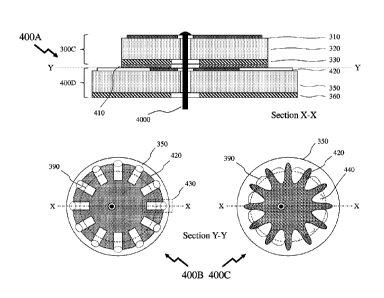
[0044] Referring to Figure 4 there is depicted a cross-section 400A of a dual
band stacked patch
antenna (DB-SPA) according to an embodiment of the invention along a section X-
X together
with first and second cross-sectional plan views 400B and 400C of the lower
patch antenna
elements along a section Y-Y. Within each of the first and second plan views
400B and 400C the
second dielectric 350 is again depicted together with the periphery 390 of the
first dielectric 320
of the upper patch antenna element 300C, as depicted by the dashed circles.
However, now the
upper metallization 420 of the lower antenna element 400D has a geometrically
varying
periphery comprising castellations defined by first and second notches 430 and
440 respectively
in the first and second cross-sectional plan views 400B and 400C respectively.
The increased
length of the periphery of the upper metallization 420 of antenna 400D results
in a lower
resonant frequency for the lower antenna element 400D. However according to
prior art, the first
lower metallization 330 of the upper element 300C cannot project beyond the
geometrically
varying periphery of the immediately adjacent second upper metallization 420,
otherwise the
castellations would effectively be shorted in an electromagnetic sense by
first lower metallization
330, thereby rendering the castellations of the second upper metallization 420
ineffective. As
such the lowest frequency that the lower patch antenna element 400D could
resonate is defined
by the overlap of the first lower metallization 330 of the upper patch antenna
element 300C over
the upper metallization 420 of the lower antenna element 400D rather than the
periphery of the
upper metallization 420 of the lower antenna element 400D alone. Also depicted
is RF feed 4000
which is coupled to the first upper metallization 310 and second upper
metallization 420 via
overlapping near-field responses. Whilst the upper patch antenna element 300C
is depicted in
Figure 4 as having a smaller diameter than the lower patch antenna element
400D its diameter
may be increased towards that of the lower patch antenna element 400D, equal
to the lower patch
antenna element 400D, or larger than the lower patch antenna element 400D.
[0045] Accordingly, the inventors provide a spacer 410 having a dielectric
constant lower than
either of the dielectric constants of upper element 300C and 400D, disposed
between the upper
element 300C and the lower element 400D. By this means the microwave signals
propagating
within lower element 400D and flowing on second upper metallization 420 are
decoupled from
first lower metallization 330. Accordingly, the geometrically varying
periphery comprising
- 12 -
Date Recue/Date Received 2020-07-30
castellations defined by first and second notches 430 and 440 respectively in
the first and second
plan views 400B and 400C respectively can now extend under the upper patch
antenna element
300C allowing the lower patch antenna element 400D to operate at lower
frequencies than prior
art DB-SPAs. The coupling between the microwave signals propagating within the
upper
metallization 420 of the lower patch antenna element 400D to the upper patch
antenna element
being reduced to below a threshold such that the resonant frequency of the
lower patch antenna
element is determined by the cavity resonator comprised of the castellated
upper metallization
420 and the ground plane metallization 360 of the second dielectric 350. The
dielectric spacer
410 is manufactured from a material having a lower effective dielectric
constant so that the
decoupling between the lower metallization 330 of the upper patch antenna
element 300C and
upper metallization 420 of the lower patch antenna element 400D is achieved
for a small or low
thickness of the dielectric spacer 410.
[0046] Referring to Figure 5 there is depicted an assembled DB-SPA according
to an
embodiment of the invention denoting the upper patch antenna element 300C,
lower patch
antenna element 400D, with the spacer 410, which is not evident. In Figure 6
there are depicted
first to third images 600A to 600C of the DB-SPA elements according to an
embodiment of the
invention. In first image 600A the upper surface of the lower patch antenna
element 400D is
depicted together with the upper surface of the upper patch antenna element
300C and spacer
410. In second image 600B the upper patch antenna element 300C is now depicted
upside down
so that the ground plane can be seen on the lower surface. In third image 600C
the lower patch
antenna element 400D is depicted with the spacer 410 and upper patch antenna
element 300C
atop it during assembly.
[0047] It would be evident from first to third images 600A to 600C
respectively and Figure 5
that the DB-SPA as depicted has a pair of electrical feeds, these being
identified in Figure 5 as
first and second feeds 500A and 500B respectively. Accordingly, signals
coupled to / from the
DB-SPA via first and second feeds 500A and 500B respectively are in quadrature
with respect to
one another for circularly polarized signals.
[0048] Referring to Figure 7 there are depicted first to third curves 710 to
730 respectively are
depicted over the frequency range 1.1 GHz ¨ 1.7 GHz for a DB-SPA designed with
an upper
patch antenna element operating within the GPS Li band and a lower patch
antenna element
employing a "castellated" periphery designed to operate within the GPS L5
band. First curve 710
- 13 -
Date Recue/Date Received 2020-07-30
representing the scenario where no spacer is employed whereas second and third
curves 720 and
730 respectively represent the use of spacers with increasing thicknesses
respectively. Also
depicted are the Li, L2, and L5 bands for the GPS GNSS system. Accordingly, as
expected the
spacer has minimal effect upon the Li response for the upper patch antenna
element but the
frequency response of the lower element shifts to lower frequencies with
increasing spacer
thickness as the effect of the lower ground metallization of the upper patch
antenna element is
reduced. The use of high dielectric materials for the dielectric of the upper
and lower patch
antennas reduces the required patch element dimensions and results in the
electric lines of force
being confined within the patch antennas. Accordingly, decoupling of the upper
patch antenna
from the lower patch antenna with the low dielectric constant spacer does not
degrade the near
field coupling of the patch antennas to the microwave feed or feeds.
[0049] A similar situation is evident in Figure 8 wherein there are depicted
first to third curves
810 to 830 respectively over the frequency range 1.1 GHz ¨ 1.7 GHz for a DB-
SPA designed
with an upper patch element operating within the GPS Li band and a lower patch
antenna
element employing a "castellated" periphery designed to operate within the GPS
L5 band. First
curve 810 representing the scenario where no spacer is employed whereas second
and third
curves 820 and 830 respectively represent the use of spacers with increasing
thickness. Also
depicted are the Li, L2, and L5 bands for the GPS GNSS system. Accordingly, as
expected the
spacer has minimal effect upon the Li response for the upper patch antenna
element but the
frequency response of the lower element shifts to lower frequencies with
increasing spacer
thickness as the effect of the lower metallization of the upper patch antenna
element is reduced.
[0050] Within the descriptions supra in respect of Figures 4 to 8 the DB-SPA
according to
embodiments of the invention has been described and depicted as being
circular. However, it
would be evident that within other embodiments of the invention the geometry
of either the
upper patch antenna element and/or lower patch antenna element may be non-
circular and have a
geometry such as elliptical, square, rectangular, a regular polygon, an
irregular polygon, and an
arbitrary geometry. Optionally, the geometry of the upper patch antenna
element and lower patch
antenna element may be the same, e.g. both square, or they may be dissimilar,
e.g. a square upper
patch antenna element with a rectangular lower patch antenna element.
[0051] Two examples being depicted in Figure 9 in first and second images 900A
and 900B
respectively. In Figure 9 in first image 900A the lower patch antenna element
body 910 is
- 14 -
Date Recue/Date Received 2020-07-30
depicted together with its upper surface metallization 920 and the footprint
of the upper patch
antenna element by line 930. In this instance each of the lower patch antenna
element and upper
patch antenna element are octagonal. In contrast within second image 900B the
lower patch
antenna element body 940 is depicted as square together with its upper surface
metallization 950
whilst the footprint of the upper patch antenna element denoted by line 960 is
rectangular. As
depicted the "castellations" on the upper surface metallization 950 in this
instance extend to
different "depths" within the footprint of the upper patch antenna element on
two sides of the
lower patch antenna element versus the other two sides. Optionally, within
other embodiments of
the invention the "castellations" may have a single "depth" or multiple
depths. The patch antenna
elements depicted in first and second images 900A and 900B are circularly
symmetric for use
with circularly polarized signals. However, within other embodiments of
invention with non-
circularly polarized signals the patch antenna elements may be non-circularly
symmetric.
[0052] Specific details are given in the above description to provide a
thorough understanding of
the embodiments. However, it is understood that the embodiments may be
practiced without
these specific details.
[0053] The foregoing disclosure of the exemplary embodiments of the present
invention has
been presented for purposes of illustration and description. It is not
intended to be exhaustive or
to limit the invention to the precise forms disclosed. Many variations and
modifications of the
embodiments described herein will be apparent to one of ordinary skill in the
art in light of the
above disclosure. The scope of the invention is to be defined only by the
claims appended hereto,
and by their equivalents.
- 15 -
Date Recue/Date Received 2020-07-30