Note: Descriptions are shown in the official language in which they were submitted.
NG(ES)026895 WO ORD
CONTROLLING A STATE OF A QUBIT ASSEMBLY VIA TUNABLE COUPLING
RELATED APPLICATIONS
[0001] This application claims priority from U.S. Patent Application
Serial
No. 15/886602, filed 1 February 2018.
[0002] This invention was made with Government support. The Government has
certain rights in this invention.
TECHNICAL FIELD
[0003] The present invention relates generally to quantum computing
systems,
and more particularly to a managing a state of a qubit assembly.
BACKGROUND
[0004] A classical computer operates by processing binary bits of
information that
change state according to the laws of classical physics. These information
bits can be
modified by using simple logic gates such as AND and OR gates. The binary bits
are
physically created by a high or a low energy level occurring at the output of
the logic
gate to represent either a logical one (e.g., high voltage) or a logical zero
(e.g., low
voltage). A classical algorithm, such as one that multiplies two integers, can
be
decomposed into a long string of these simple logic gates. Like a classical
computer, a
quantum computer also has bits and gates. Instead of using logical ones and
zeroes, a
quantum bit ("qubit") uses quantum mechanics to occupy both possibilities
simultaneously. This ability means that a quantum computer can solve a large
class of
problems with exponentially greater efficiency than that of a classical
computer.
SUMMARY
[0005] In accordance with one example, a qubit apparatus is provided. The
qubit
apparatus includes a load, a qubit, and a compound Josephson junction coupler
coupling the qubit to the load. A coupling controller controls the coupling
strength of the
compound Josephson junction coupler such that a coupling between the gun and
the
-1-
Date Recue/Date Received 2023-04-12
CA 03088449 2020-07-13
WO 2019/152242 PCT/US2019/014796
load is a first value when a reset of the qubit is desired and a second value
during
operation of the qubit.
[0006] In accordance with another example, a method is provided for
operating a
qubit. A first value of a control flux is provided to a tunable coupler
linking the qubit and
a dissipative element such that the qubit is substantially isolated from the
dissipative
element. A quantum operation is performed at the qubit. A second value of the
control
flux is provided to the tunable coupler such that the qubit is coupled to the
dissipative
element. A reset time is allowed to elapse while the qubit relaxes to a ground
state
while coupled to the dissipative element.
[0007] In accordance with a further example, a qubit apparatus is
provided. The
qubit apparatus includes a load, comprising a circuit element having an
impedance with
a non-vanishing real part, a qubit, a compound Josephson junction coupler
coupling the
qubit to the load. A coupling controller controls the coupling strength of the
compound
Josephson junction coupler such that a coupling between the qubit and the load
is a first
value, providing a strong coupling between the qubit and the load, when a
reset of the
qubit is desired and a second value, the second value represents substantial
isolation of
the qubit from the load, during operation of the qubit.
BRIEF DESCRIPTION OF THE DRAWINGS
[0008] FIG. 1 illustrates a functional block diagram of a qubit assembly
in
accordance with an aspect of the present invention:
[0009] FIG. 2 illustrates a schematic of one example of a circuit for
reading a
state of a qubit;
[0010] FIG. 3 is a line chart illustrating the variation of the mutual
inductance
between the qubit and the resistive load, represented in picohenries on the
vertical axis,
as a function of a provided control flux, represented on the horizontal axis
in units of the
magnetic flux quantum;
[0011] FIG. 4 is a line chart illustrating a projected relaxation time of
a qubit,
represented logarithmically in nanoseconds on the vertical axis, as a function
of a
provided control flux, represented on the horizontal axis in units of the
magnetic flux
quantum;
-2-
CA 03088449 2020-07-13
WO 2019/152242 PCT/US2019/014796
[0012] FIG. 5 is a line chart illustrating the measured lifetime, 7-1, of
a qubit,
represented logarithmically in microseconds on the vertical axis, as a
function of a
provided control flux, represented on the horizontal axis 504 in units of the
magnetic flux
quantum;
[0013] FIG. 6 is a line chart comparing the evolution of the population
of the
excited state for a qubit after an excitation pulse; and
[0014] FIG. 7 illustrates one example of a method for operating a qubit.
DETAILED DESCRIPTION
[0015] Solid state quantum bits ("qubits") encode information in
quantized
excitations of a macroscopic degree of freedom in objects such as
semiconducting
quantum dots, SQUIDs, or other superconducting devices. In any quantum
computer, it
is desirable to initialize the quantum bits to a known state with high
fidelity. In some
architectures, the physical qubits can be recycled throughout the computation,
such that
the application is sensitive to the speed of the reset operation. A solid
state qubit, in
accordance with an aspect of the present invention, has the ability to
initialize the
system in a known state with high fidelity, a process referred to herein as a
"reset" of the
qubit. In one implementation, the qubit is initialized in the ground state. A
related
process is the removal of unwanted thermal excitations from the qubit. In this
process,
referred to herein as "cooling" the qubit, the excited state population of the
qubit is
reduced to below thermal levels.
[0016] The present disclosure relates generally to superconducting
circuits, and
more particularly to a fast reset or cooling scheme that involves coupling the
qubit to a
dissipative environment via a tunable coupler, allowing for selective reset or
cooling of
the qubit. It is often desirable to reuse a qubit in an algorithm, which is
expedited by an
efficient method for initializing the qubit in the ground state. Since long
qubit lifetimes
are also desirable, it is intractable to wait out the qubit lifetime to allow
the qubit to
decay naturally. Therefore, a method is provided for qubit reset that can
initialize the
qubit quickly, but will not deleteriously affect the qubit lifetime during
operation. An
external bias tunes the coupling between the qubit and the environment, with
the bias
idling at a point such that the qubit is isolated from the environment,
preserving the qubit
-3-
CA 03088449 2020-07-13
WO 2019/152242 PCT/US2019/014796
lifetime. Fast DC pulses on the external bias are used to activate the coupler
when it is
desirable to reset the qubit.
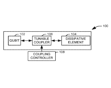
[0017] FIG. 1 illustrates a functional block diagram of a qubit assembly
100 in
accordance with an aspect of the present invention. The qubit assembly 100
comprises
a qubit 102 coupled to a dissipative element 104 via a tunable coupler 106.
The
qubit 102 can include any physical assembly having a plurality of energy
states that are
tunable in response to a control mechanism (not shown). For example, the qubit
cell
can be implemented as an oscillator that can transfer energy between some
combination of an electric field of a capacitor, a magnetic field of an
inductor, and one or
more superconducting Josephson junctions, such that the qubit cell can include
one or
more of a charge qubit, a flux qubit, and a phase qubit. Exemplary
implementations of a
qubit cell can include one or more of a Josephson junction, a quantum dot, a
SQUID
(superconducting quantum interference device), a Cooper pair box, and an ion
trap. It
will be further appreciated that the term "coupled" is intended to encompass
not only a
means of physical coupling, such as a mechanical coupling by means of an
electrical
conductor, but also any other appropriate coupling means including capacitive,
inductive, magnetic, nuclear, and optical coupling, or any combination of the
foregoing.
[0018] The tunable coupler 106 can include any appropriate structure for
selectively isolating the qubit 102 from the dissipative element 104. In one
implementation, the tunable coupler is an RF-SQUID with a small inline DC-
SQUID,
known as a compound Josephson junction (CJJ), which acts as a tunable mutual
inductance between two elements 102 and 104. The magnetic susceptibility of
the
coupler can be tuned by applying flux to either the main inductor of the RF-
SQUID or to
the CJJ. Using this coupler 106, a tunable mutual inductance can be changed in
situ.
The tunable coupler 106 can be controlled via a coupling controller 108 that
controls the
coupling strength of the compound Josephson junction. For example, the
coupling
controller 108 can tune the mutual coupling at the tunable coupler 106 between
a first
value, representing a strong coupling between the qubit 102 and the
dissipative
element 104, for example, a mutual inductance between twenty and four hundred
fifty
picohenries, and a second value, representing substantial isolation of the
qubit from the
dissipative element, such as a mutual inductance near zero. The coupling
-4-
CA 03088449 2020-07-13
WO 2019/152242 PCT/US2019/014796
controller 108 can utilize single flux quantum (SFQ) logic (e.g., reciprocal
quantum logic
(ROL) logic), and/or conventional logic. In one implementation, one or more
fast DC
pulses can be applied via a coupler control line (not shown) to turn on the
coupler and
reset the qubit. During qubit operation, the coupler will be DC biased and
held in a state
providing near zero coupling. This allows for a controllable reset of the
qubit 102 to the
ground state quickly without having an undesired, deleterious effect on the
qubit
lifetime.
[0019] In one implementation, the dissipative element 104 can comprise a
circuit
element, referred to herein as a load, that receives the energy stored in the
qubit 102
when the mutual coupling between the qubit and the dissipative element is
strong.
Essentially the qubit control 108 can tune the qubit 102 to discharge its
associated
quantum state along the tunable coupler 106 to provide it to the circuit
element. In such
a case, the dissipative element 104 can comprise any element having a non-
vanishing
real impedance to which it is desirable to provide a single photon input. For
example,
said circuit element can be an amplifier, a detector, a fiber coupler, an opto-
modulator, a
beam splitter, or similar component. It will further be appreciated that the
qubit
assembly 100 can be used with resonators, other qubits, or other qubit
assemblies
having the fast cooling and reset configuration of the illustrated qubit
assembly.
[0020] FIG. 2 illustrates a schematic of one example of a circuit 200 for
reading a
state of a qubit. The circuit 200 includes a transmon qubit 210, a readout
resonator 214, a feedline 216, a transmission line 218, a resistive load 219,
and a
tunable compound Josephson junction (CJJ) coupler 220, comprising a
superconducting loop interrupted by a CJJ 222 to form a radio frequency (RF)
superconducting SQUID. The tunable compound Josephson junction (CJJ) coupler
220
includes a first inductor 224 in the superconducting loop that provides a
mutual
inductance. N1,7, to the qubit 210 via a galvanic connection, and a second
inductor 226
that provides a mutual inductance, iç, to the transmission line 218 leading to
the
resistive load 219 via a galvanic connection. In the illustrated
implementation, the
CJJ 222 includes two identical Josephson junctions 228 and 229.
[0021] A flux, cP.õ, can be applied to the CJJ 222 by applying current to
a control
line 232, with a bias tee 234 on the control line available to allow for both
DC and
-5-
CA 03088449 2020-07-13
WO 2019/152242 PCT/US2019/014796
pulsed signals to be applied to the coupler. Since current provided to the
control
line 232 does not generate current in the superconducting loop when the
junctions 228
and 229 in the CJJ 222 are identical, the qubit 210 is protected from
dissipation caused
by this line. The coupler represents an effective mutual inductance, M,ff = Mq
Mrx,
where ;If is the magnetic susceptibility of the coupler. The magnetic
susceptibility is a
function of the flux applied to the CJJ 222, which can be expressed as:
fie (4),)
Eq. 1
[0022] where it is assumed that L is the total geometrical inductance of
the
27cL _______________ õ 124),
coupler, fl,õ ((Da) = cos 4)0 , cl)c, is the magnetic flux quantum,
approximately
equal to 2.07 femtowebers, and I is the combined critical current of the two
junctions in
the CJJ 222.
[0023] Using the control line 232, the effective mutual inductance, Act,-
, between
the qubit 210 and the resistive load 219 can be tuned to allow for selective
reset of the
qubit state. Since the qubit lifetime is a function of this mutual inductance,
we isolate
the qubit from the environment by setting :14,.ff = 0 and reset it by turning
up ,".4%. The
dependence of the qubit lifetime, Tr, with the bias, cba, applied to the
coupler can be
seen in Eq. 2:
Ti (430 = zecQ ____
= Mali (4:ka ))2
Eq. 2
[0024] where Cq represents a capacitance of the qubit 210, Lq represents
an
inductance of the qubit, and Zo represents an impedance of the dissipative
element,
such as the resistive load 219.
[0025] FIG. 3 is a line chart 300 illustrating the variation of the
mutual inductance
between the qubit 210 and the resistive load 219, represented in picohenries
on the
vertical axis 302, as a function of the control flux provided to the CJJ 222,
represented
on the horizontal axis 304 in units of the magnetic flux quantum. For the
purposes of
the model illustrated in FIG. 3, it is assumed that Mq is one hundred
picohenries. From
the plotted line 306. it can be seen that that the coupling at (tk,.õ = (boa
is zero, due to
-6-
CA 03088449 2020-07-13
WO 2019/152242 PCT/US2019/014796
the fact that x goes to 0. For 4,13/2 <(Pa <4, X takes on a negative value and
eventually grows to be much larger, in absolute terms, than it was at cl)õ =
0. In one
implementation. this large negative coupling can be exploited to give an
enhancement
in the absolute coupling strength. When gate operations are performed on the
qubit 210, the coupler 220 is turned off by providing a control flux, 4,õ =
412 so that
the qubit is isolated from the resistive load 219 and the lifetime of the
qubit is not
reduced. For reset, a voltage pulse is applied to the I, line at the bias tee
234 such that
the control flux, ct.õ, is raised to 4,0, thus turning the coupler 220 on. In
order to reduce
the effects of capacitors on the bias line, the readout can be followed with a
negative
pulse of equal magnitude on the line.
[0026] FIG. 4 is a line chart 400 illustrating a projected relaxation
time of the
qubit 210, represented logarithmically in nanoseconds on the vertical axis
402, as a
function of the control flux provided to the CJJ 222, represented on the
horizontal
axis 404 in units of the magnetic flux quantum. For the purposes of the model
illustrated in FIG. 4, it is assumed that Mq is one hundred picohenries, an
energy of the
ground to excited transition of the qubit is 9 GHz, an impedance of the
resistive load
is 50 0, and a capacitance of the qubit is 60 fF. From the plotted line 406,
it can be
seen that that the relaxation time is maximized at 4), = 4,0/2 and cl),
=3430/2, where
the coupling between the qubit 210 and the dissipative element is minimized.
The
relaxation time is minimized at (4), , where the coupling is maximized.
[0027] FIG. 5 is line chart 500 illustrating the measured lifetime, TI,
of the
qubit 210, represented logarithmically in microseconds on the vertical axis
502, as a
function of the control flux provided to the CJJ 222, represented on the
horizontal
axis 504 in units of the magnetic flux quantum. From the plotted line 506, it
can be seen
that a maximum lifetime of 2.2 is was achieved when the qubit 210 was isolated
from
the dissipative element and a minimum lifetime of 2 ns was achieved during
reset.
Accordingly, the qubit lifetime, in this specific implementation, is reduced
by a factor of
approximately one thousand, although depending on the implementation, the
lifetime
can be shortened by a factor of between five-hundred and five-thousand. The
method
-7-
CA 03088449 2020-07-13
WO 2019/152242 PCT/US2019/014796
appears to be capable of resetting the qubit 210 with at least 99.9% fidelity
in less
than 20 ns.
[0028] The proposed device has been tested via a four-frame measurement
intended to reduce the effect of low frequency drift in the readout signal.
One frame
was a simple Ti decay in which the qubit 210 was Tr-pulsed and some time was
allowed
to lapse before measurement. This is referred to as the "no-reset" case in
FIG. 6 below.
The second was a measurement of the qubit when no -rr pulse was applied, with
some
time allowed to elapse before measurement. In a third frame, the qubit 210 was
1T-
pulsed, and a pulse was applied to the reset coupler that set ,1)õ, = 4õ for
some time
before measuring. This is referred to as the "reset" case in FIG. 6 below. In
a fourth
case, the qubit was not excited, but a pulse was still applied to the reset
coupler. The
magnitude of the integrated transmitted signal through the readout resonator
feedline
was measured for 1 million samples of the four frames when the reset/wait time
was set
to 3.5 ns. The reset signal had a 1 ns turn on and turn off with an error
function profile,
so the shortest delay for all measurements was 2 ns and this 2 ns is included
in the
reset/wait time.
[0029] The measurements were performed using high-power readout, so the
readings separated into two distributions due to the bright state behavior of
the readout
resonator, with the -bright state counts" in one distribution representing a
measure of 11)
state population. As expected, the bright state counts were highest when an
excitation
pulse was applied to the qubit, although it will be noted that even when no
excitation
pulse is applied to the qubit there are some counts in the "bright state"
distribution, and
the number obtained in the no excitation and no reset frame provides a
baseline for the
differencing measurement used below. The reset provides a significant drop in
the
bright state counts when the qubit 210 has been excited, and even a slight
reduction in
the peak of the distribution for the non-excited case.
[0030] FIG. 6 is a line chart 600 comparing the evolution of the
population of the
excited state for a qubit after an excitation pulse. A vertical axis 602
represents the
fractional population of the excited state, on a logarithmic scale, and the
horizontal
axis 604 represents time, in nanoseconds. on a logarithmic scale. A first
plotted
line 606 represents the no-reset case and the second plotted line 608
represents the
-8-
CA 03088449 2020-07-13
WO 2019/152242 PCT/US2019/014796
reset case. The data for each case is normalized to the difference between the
no reset
measurement and the no excitation with reset measurement taken with a 100 ns
reset
time. It will be appreciated that the reset curve decays to the noise floor of
the
measurement by 10 ns, as would be expected for a T1 equal to 2 ns.
Unfortunately, the
noise on the measurement is such that although some measurements at reset
times
of >10 ns fall below 0.1%, the scatter in the data gives an error bar of about
0.5%.
[0031] In view of the foregoing structural and functional features
described
above, an example method will be better appreciated with reference to FIG. 7.
While,
for purposes of simplicity of explanation, the example method of FIG. 7 is
shown and
described as executing serially, it is to be understood and appreciated that
the present
examples are not limited by the illustrated order, as some actions could in
other
examples occur in different orders, multiple times and/or concurrently from
that shown
and described herein. Moreover, it is not necessary that all described actions
be
performed to implement a method.
[0032] FIG. 7 illustrates one example of a method 700 for operating a
qubit.
At 702, a first value of a control flux is provided to a tunable coupler
linking the qubit and
a dissipative element such that the qubit is substantially isolated from the
dissipative
element. In one example, the tunable coupler includes a superconducting loop
interrupted by a compound Josephson junction, and the first value of the
control flux is
provided to the compound Josephson junction. At 704, a quantum operation is
performed at the qubit. At 706, a second value of the control flux is provided
to the
tunable coupler such that the qubit is coupled to the dissipative element. In
one
implementation, the first value of the control flux is substantially equal to
one-half of a
flux quantum, and the second value of the control flux is greater than one-
half of a flux
quantum and less than or equal to the flux quantum. The second value of the
control
flux can be selected to provide a strong, negative coupling between the qubit
and the
dissipative element. At 708, a reset time is allowed to elapse while the qubit
relaxes to
a ground state during coupling to the dissipative element. The reset time can
be
between 5 ns and 20 ns, and in one implementation, a reset time substantially
equal
to 10 ns can be used.
-9-
CA 03088449 2020-07-13
WO 2019/152242 PCT/US2019/014796
[0033] What have been described above are examples. It is, of course, not
possible to describe every conceivable combination of components or
methodologies,
but one of ordinary skill in the art will recognize that many further
combinations and
permutations are possible. Accordingly, the disclosure is intended to embrace
all such
alterations, modifications, and variations that fall within the scope of this
application,
including the appended claims. As used herein, the term "includes" means
includes but
not limited to, the term "including" means including but not limited to. The
term "based
on" means based at least in part on. Additionally, where the disclosure or
claims recite
"a," "an," "a first," or "another" element, or the equivalent thereof, it
should be
interpreted to include one or more than one such element, neither requiring
nor
excluding two or more such elements.
-10-