Note: Descriptions are shown in the official language in which they were submitted.
CA 03089494 2020-07-24
REDUNDANT ENERGY ACQUISITION CIRCUIT OF POWER MODULE,
AND CONTROL METHOD THEREOF
Technical Field
[0001] The present application relates to the technical field of power
electronics, in particular to a redundant energy acquisition circuit of a
power module
and a control method thereof.
Background
[0002] The voltage source converter technique is a novel conversion
technique based on turn-off device IGBTs (insulated gate bipolar transistors)
and the
1() PWM (pulse width modulation) technique. Two-level converters consisting
of IGBTs
have been widely applied on low-voltage occasions. To solve the problems of
large
equipment stress and system loss, loud noise and harsh electromagnetic
environments
caused by high-frequency jumps of the output voltage of the two-level
converters,
three-level voltage source converters are developed to expand the application
of
voltage source converters in the aspect of voltage level and capacity.
[0003] With the emergence of modular multilevel converters (MMCs),
multilevel converters, with the voltage level reaching hundreds of kilovolts
and the
capacity up to thousands of watts, have been successfully applied to the field
of
flexible direct-current transmission.
[0004] The voltage source converters are formed by series connection of a
large number of power modules. When one power module malfunctions, a bypass
switch is closed to remove the malfunctioned unit to fulfill non-stop
operation of a
system.
[0005] The inventor finds that if an energy acquisition board in the power
modules fails, a control board will not be able to operate normally, and the
trigger
circuit of the bypass switch cannot function, the power module cannot be
successfully
1
Date Regue/Date Received 2020-07-24
CA 03089494 2020-07-24
bypassed, and thus, the system has to be stopped. Thus, how to improve the
energy
acquisition reliability of the power modules and guarantee reliable closing of
the
bypass switch has become the key technical factor for improving the
reliability of
voltage source converter equipment.
[0006] Chinese Invention Patent Application No.CN201710228027.X
provides a self-trigger circuit for a bypass switch of a multilevel converter
sub-module, wherein a capacitor of the bypass switch is charged by the voltage
across
the two ends of the bypass switch to provide closing energy for the bypass
switch.
Essentially, the bypass switch capacitor Cc is connected in series with a
resistor R1
and is then connected in parallel with a sub-module capacitor Csm to form this
circuit.
Due to the fact that the capacitance of the bypass switch capacitor is
generally
hundreds of microfarad and the capacitance of the sub-module capacitor Csm is
generally several millifarads to tens of millifarads, it is difficult to
charge the bypass
switch capacitor to a rated value without causing overvoltage of the sub-
module
capacitor. In addition, if a sub-module energy acquisition power supply
malfunctions,
a sub-module control board will not be able to operate or to provide a bypass
switch
closing instruction. In this case, if a normally-closed switch is connected to
the loop
of the bypass switch capacitor and a contact control end, the bypass switch
capacitor
will be short-circuited and cannot be charged. Hence, this solution has the
risks of
overvoltage damage to the sub-module capacitor and failure to close the bypass
switch when the sub-module energy acquisition power supply malfunctions.
Summary
[0007] The objective of the invention is to provide a redundant energy
acquisition circuit of a power module and a control method thereof. The
redundant
energy acquisition circuit is applied to voltage source converters to provide
another
energy acquisition path when the energy acquisition board of a power module of
a
converter malfunctions and to ensure that the bypass switch of the power
module can
be reliably closed, thus lowering the probability of system shutdown and
having good
2
Date Regue/Date Received 2020-07-24
CA 03089494 2020-07-24
economical and technical performance.
[0008] The embodiments of the present application provide a redundant
energy acquisition circuit of a power module. The power module comprises at
least
one power semiconductor device, a first capacitor and a first bypass switch,
and is
characterized in that the redundant energy acquisition circuit of the power
module
comprises a power supply board, a first charging circuit, a control board and
a
discharge circuit, wherein the power supply board acquires energy from the
first
capacitor, supplies power to the control board and charges the discharge
circuit; the
first charging circuit has one end connected to a positive electrode of the
first
capacitor and another end connected to the discharge circuit, and charges the
discharge circuit when the power supply board is not operating normally; the
control
board controls the discharge circuit to close; and the discharge circuit
discharges and
triggers the first bypass switch to close being closed.
[0009] Furthermore, the redundant energy acquisition circuit of the power
module further comprises a second charging circuit, wherein the second
charging
circuit is connected in parallel with the first capacitor and triggers the
discharge
circuit to close when the control board is not operating normally.
[0010] Furthermore, the second charging circuit comprises a second
stabilivolt and a second resistor, wherein a cathode of the second stabilivolt
is
connected to the positive electrode of the first capacitor, the second
resistor has one
end connected to an anode of the second stabilivolt and another end connected
to a
negative electrode of the first capacitor, and after the second stabilivolt is
broken
down, the discharge circuit is closed.
[0011] Furthermore, the redundant energy acquisition circuit of the power
module further comprises a fourth switch, wherein the fourth switch is
connected in
series between a negative electrode of the discharge circuit and the negative
electrode
of the first capacitor where the power supply board is an isolation-type power
supply
3
Date Recue/Date Received 2020-07-24
CA 03089494 2020-07-24
board.
[0012] Furthermore, the discharge circuit comprises a second capacitor and
a second switch, wherein the second capacitor has a positive electrode
connected to
the power supply board and the first charging circuit and a negative electrode
connected to a ground of the power supply board, and is charged by the power
supply
board or the first charging circuit; the second switch has one end connected
to a
positive electrode of the second capacitor and another end connected to a
control end
of the first bypass switch; and after the second switch is closed, the second
capacitor
discharges and triggers the first bypass switch to close.
ft) [0013]
Furthermore, the first charging circuit comprises a first stabilivolt
and a first resistor, wherein a cathode of the first stabilivolt is connected
to the
positive electrode of the first capacitor, and the first resistor has one end
connected to
an anode of the first stabilivolt and another end connected to the positive
electrode of
the second capacitor.
[0014] Furthermore, the first charging circuit further comprises a third
switch, which is connected to the first charging circuit in series and
controls the first
charging circuit to open or close.
[0015] Furthermore, the discharge circuit further comprises a third resistor,
wherein the third resistor is connected in parallel with the second capacitor,
the
resistance of the third resistor is adjustable, and the charging voltage can
be controlled
by voltage division of the third resistor and the first resistor.
[0016] Furthermore, the discharge circuit further comprises a third
stabilivolt being connected in parallel with the second capacitor and being
able to
stabilize a charging voltage.
[0017] Furthermore, the second switch, the third switch and the fourth
switch are one or more of mechanical switches, relays, thyristors, IGBTs,
IGCTs,
4
Date Recue/Date Received 2020-07-24
CA 03089494 2020-07-24
GTOs and MOSFETs.
[0018] The embodiments of the present invention further provide a control
method of a redundant energy acquisition circuit of a power module. The
control
method is implemented, when a power module malfunctions and needs to be
bypassed, to allow a power supply board to acquire energy from a first
capacitor, to
supply power to a control board and to charge a discharge circuit, wherein the
method
comprises the following steps: charging the discharge circuit by a first
charging
circuit when the power supply board is not operating normally; controlling the
discharge circuit to close by the control board; and discharging and
triggering a first
bypass switch to close after the discharge circuit is closed.
[0019] Furthermore, the method further comprises the following step:
triggering the discharge circuit to close by a second charging circuit when
the control
board is not operating normally.
[0020] Furthermore, before the step of charging the discharge circuit by a
first charging circuit when the power supply board is not operating normally,
the
method further comprises the following step: locking each drive instruction of
the
power module when the power module malfunctions during normal operation.
[0021] Furthermore, the step of charging the discharge circuit by the first
charging circuit comprises: breaking down the first stabilivolt when a first
capacitor
voltage of the first capacitor reaches a first threshold of a first
stabilivolt; and
charging a second capacitor by the first capacitor through the first
stabilivolt and a
first resistor.
[0022] Furthermore, the step of controlling the discharge circuit to close by
the second charging circuit instead of the control board comprises: continuing
to
charge the first capacitor until a voltage of the first capacitor reaches a
second
threshold of a second stabilivolt, breaking down the second stabilivolt, and
triggering
a second switch to close.
5
Date Regue/Date Received 2020-07-24
CA 03089494 2020-07-24
[0023] According to the redundant energy acquisition circuit of the power
module according to the embodiments of the present application, when an energy
acquisition board of the power module malfunctions, the redundant energy
acquisition
circuit can store energy for a closing circuit of the bypass switch to ensure
that the
bypass switch has sufficient closing energy; and through the dual
configurations of
energy storage in the closing circuit of the bypass switch and triggering a
closing
instruction, the reliability of successful bypassing is improved, the switch
module and
the capacitors are protected against damage under an overvoltage condition,
and
forced shutdown of the converter is avoided.
Brief Description of the Drawings
[0024] To more clearly illustrate the technical solutions of the embodiments
of the present application, the accompanying drawings required for the
description of
the embodiments are briefly introduced below. Obviously, the drawings in the
following description are merely for some embodiments of the present
application,
and those ordinarily skilled in the art can obtain other drawings according to
the
following ones without paying creative effort.
[0025] FIG. 1A is a composition diagram of a power module according to
one embodiment of the present application;
[0026] FIG. 1B is a composition diagram of a power module according to
another embodiment of the present application;
[0027] FIG. 1C is a composition diagram of a power module according to
another embodiment of the present application;
[0028] FIG. 1D is a composition diagram of a power module according to
yet another embodiment of the present application;
[0029] FIG. 2 is an application diagram of an energy acquisition circuit of
power modules according to one embodiment of the present application;
6
Date Recue/Date Received 2020-07-24
CA 03089494 2020-07-24
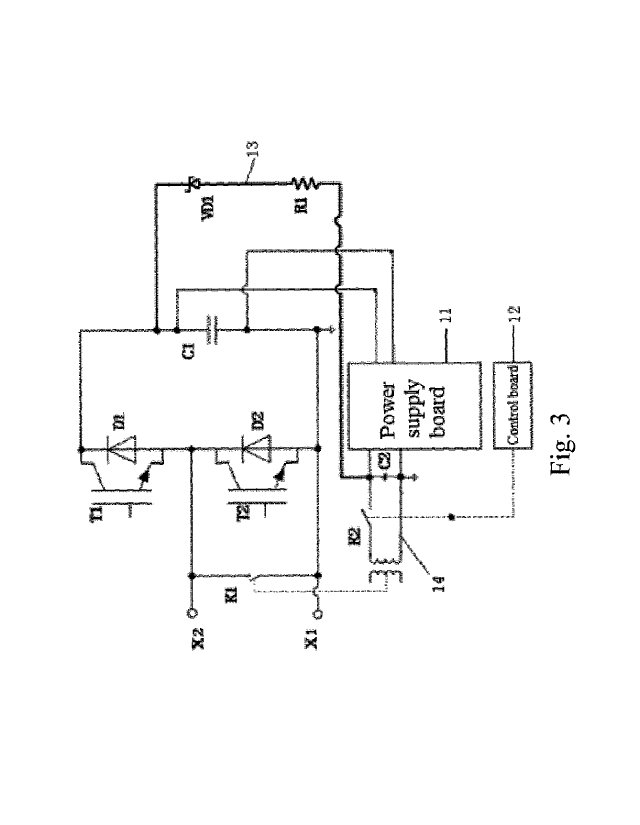
[0030] FIG. 3 is a composition diagram of a redundant energy acquisition
circuit of a power module according to one embodiment of the present
application;
[0031] FIG. 4 is a composition diagram of a redundant energy acquisition
circuit of a power module according to another embodiment of the present
application;
[0032] FIG. 5 is a composition diagram of a redundant energy acquisition
circuit of a power module according to another embodiment of the present
application;
[0033] FIG. 6 is a composition diagram of a redundant energy acquisition
circuit of a power module according to yet another embodiment of the present
application;
[0034] FIG. 7A is a flow diagram of a control method of a redundant
energy acquisition circuit of a power module according to one embodiment of
the
present application;
[0035] FIG. 7B is a flow diagram of the control method of the redundant
energy acquisition circuit of the power module shown in FIG. 7A of the present
application;
[0036] FIG. 8A is a flow diagram of a control method of a redundant
energy acquisition circuit of a power module according to another embodiment
of the
present application;
[0037] FIG. 8B is a flow diagram of the control method of a redundant
energy acquisition circuit of the power module shown in FIG. 8A of the present
application;
[0038] FIG. 9 is a flow diagram of a control method of a redundant energy
acquisition circuit of a power module according to another embodiment of the
present
7
Date Recue/Date Received 2020-07-24
CA 03089494 2020-07-24
application;
[0039] FIG. 10 is a flow diagram of a control method of a redundant energy
acquisition circuit of a power module according to yet another embodiment of
the
present application.
Detailed Description of Embodiments
[0040] To make the purposes, technical solutions and advantages of the
embodiments of the present application clearer, a more detailed and explicit
description of the specific implementations of the technical solutions of the
present
application will be given below on conjunction with the accompanying drawings
and
embodiments. Understandably, the specific implementations in the following
description are only for the purpose of explanation and are not intended to
limit the
present application. The embodiments in the following description are merely
illustrative ones, and are not all possible ones of the present application.
All other
embodiments obtained by those skilled in the art based on various
modifications to
the present application should also fall within the scope of the present
application.
[0041] It should be understood that the terms such as -first", -second" and
-third" adopted in this text to describe various elements or components are
not meant
to limit these elements or components, and are merely used to distinguish one
element
or component from another one. Hence, first element(s) or component(s)
discussed
hereinafter may also be referred to as second element(s) or component(s),
without
departing from the contents of the present application.
[0042] A power module comprises at least one power semiconductor
device, a first capacitor Cl and a first bypass switch Kl. Or, the power
module
comprises at least two power semiconductor devices and is of a semi-bridge
connection form. Or, the power module comprises at least four power
semiconductor
devices and is of a fully-bridged connection form. Or, the power module is of
other
circuit forms including the first capacitor Cl and the first bypass switch Kl.
FIG. 1A,
8
Date Recue/Date Received 2020-07-24
CA 03089494 2020-07-24
FIG. 1B, FIG. 1C and FIG. 1D are composition diagrams of the power module
according to the embodiments of the present application. As shown in FIG. 1A,
the
power module is of the semi-bridge connection form. As shown in FIG. 1B, the
power
module is of the fully-bridged connection form. As shown in FIG. 1C and FIG.
1D,
the power modules are of other circuit forms including the first capacitor Cl
and the
first bypass switch Kl. The first bypass switch K1 has a mechanical hold
function
after being closed, that is, the first bypass switch K1 can be kept in a
closed state after
being powered off. The closing signal of the first bypass switch K1 is from
discharge
of a second capacitor C2.
[0043] FIG. 2 is an application diagram of an energy acquisition module of
the power modules according to an embodiments of the present application. As
shown
in FIG. 2, the power modules are connected in series to form a conversion
chain of a
voltage source converter.
[0044] FIG. 3 is a composition diagram of a redundant energy acquisition
circuit of a power module according to one embodiment of the present
application.
The redundant energy acquisition circuit is applied to the power module and
comprises a power supply board 11, a control board 12, a first charging
circuit 13 and
a discharge circuit 14.
[0045] The power supply board 11 acquires energy from the first capacitor
Cl, supplies power to the control board 12, and charges the discharge circuit
14. The
first charging circuit 13 has one end connected to a positive electrode of the
first
capacitor Cl and another end connected to the discharge circuit 14, and
charges the
discharge circuit 14 when the power supply board 11 is not operating normally.
The
control board 12 controls the discharge circuit 14 to close. The discharge
circuit 14
discharges and triggers the first bypass switch K1 to close after being
closed.
[0046] The first charging circuit 13 comprises a first stabilivolt VD1 and a
first resistor Rl.
9
Date Recue/Date Received 2020-07-24
CA 03089494 2020-07-24
[0047] A cathode of the first stabilivolt VD1 is connected to the positive
electrode of the first capacitor Cl. The first resistor R1 has one end
connected to an
anode of the first stabilivolt VD1 and another end connected to a positive
electrode of
a second capacitor C2.
[0048] The discharge circuit 14 comprises the second capacitor C2 and a
second switch 1(2.
[0049] The second capacitor C2 has a positive electrode connected to the
power supply board 11 and the first charging circuit 13 and a negative
electrode
connected to a ground of the power supply board 11, and is charged by the
power
supply board 11 or the first charging circuit 13. The second switch K2 has one
end
connected to the positive electrode of the second capacitor C2 and another end
connected to a control end of the first bypass switch Kl, and after the second
switch
K2 is closed, the second capacitor C2 discharges and triggers the first bypass
switch
K1 to close.
[0050] The second switch comprises but is not limited to one of a
mechanical switch, a relay, a thyristor, an IGBT, an IGCT, a GTO and an
MOSFET.
That is, the second switch K2 may be a mechanical switch, a relay, or an
electronic
switch such as a thyristor, an IGBT, an IGCT, a GTO or an MOSFET. Wherein, a
trigger signal of the second switch K2 is from the power supply board or the
control
board.
[0051] According to the redundant energy acquisition circuit of the power
module according to this embodiment of the present application, when an energy
acquisition board of the power module malfunctions, the redundant energy
acquisition
circuit can store energy for a closing circuit of the bypass switch to ensure
that the
bypass switch has sufficient closing energy; and through the dual
configurations of
energy storage in the closing circuit of the bypass switch and triggering a
closing
instruction, the reliability of successful bypassing is improved, the switch
module and
Date Recue/Date Received 2020-07-24
CA 03089494 2020-07-24
the capacitors are protected against damage under an overvoltage condition,
and
forced shutdown of the converter is avoided.
[0052] FIG. 4 is a composition diagram of a redundant energy acquisition
circuit of a power module according to another embodiment of the present
application. As shown in FIG. 4, the redundant energy acquisition circuit is
applied to
a power module. The power module comprises at least one power semiconductor
device, a first capacitor Cl, a first bypass switch Kl. The redundant energy
acquisition circuit of the power module comprises a power supply board 11, a
control
board 12, a first charging circuit 23 and a discharge circuit 24.
[0053] The power supply board 11 acquires energy from the first capacitor
Cl, supplies power to the control board 12, and charges the discharge circuit
24. The
first charging circuit 23 has one end connected to a positive electrode of the
first
capacitor Cl and another end connected to the discharge circuit 24, and
charges the
discharge circuit 24 when the power supply board 11 is not operating normally.
The
control board 12 controls the discharge circuit 24 to close. The discharge
circuit 24
discharges and triggers the first bypass switch K1 to close after being
closed.
[0054] The first charging circuit 23 comprises a first stabilivolt VD1, a
first
resistor R1 and a third switch K3.
[0055] A cathode of the first stabilivolt VD1 is connected to the positive
electrode of the first capacitor Cl. One end of the first resistor R1 is
connected to one
end of the third switch K3, another end of the third switch K3 is connected to
an
anode of the first stabilivolt VD1, and another end of the first resistor R1
is connected
to a positive electrode of a second capacitor C2. The third switch K3 is used
to control
the first charging circuit 23 to open or close.
[0056] The discharge circuit 24 comprises the second capacitor C2, a
second switch K2 and a third resistor R3.
11
Date Recue/Date Received 2020-07-24
CA 03089494 2020-07-24
[0057] The second capacitor C2 has a positive electrode connected to the
power supply board 11 and the first charging circuit 23 and a negative
electrode
connected to a ground of the power supply board 11, and is charged by the
power
supply board 11 or the first charging circuit 23. The second switch K2 has one
end
connected to the positive electrode of the second capacitor C2 and another end
connected to a control end of the first bypass switch Kl. After the second
switch K2
is closed, the second capacitor C2 discharges and triggers the first bypass
switch K1
to close. The third resistor R3 is connected in parallel with the second
capacitor, the
resistance of the third resistor R3 is adjustable, and the charging voltage
can be
controlled by voltage division of the third resistor R3 and the first resistor
Rl.
[0058] The second switch and the third switch comprise but are not limited
to one or more of mechanical switches, relays, thyristors, IGBTs, IGCTs, GTOs
and
MOSFETs. That is, the second switch K2 and the third switch K3 may be
mechanical
switches, relays, or electronic switches such as thyristors, IGBTs, IGCTs,
GTOs or
MOSFETs. Wherein, trigger signals of the second switch K2 and the third switch
K3
are from the power supply board or the control board.
[0059] The first charging circuit further comprises the third switch K3,
which has one end connected to an anode of the first stabilivolt VD1 and
another end
connected to the first resistor Rl. The third switch K3 is in a closed state
when the
power supply board does not operate and is in an open state when the power
supply
board operates normally.
[0060] FIG. 5 is a composition diagram of a redundant energy acquisition
circuit of a power module according to another embodiment of the present
application. The redundant energy acquisition circuit is applied to a power
module.
The power module comprises at least one power semiconductor device, a first
capacitor Cl and a first bypass switch Kl. The redundant energy acquisition
circuit of
the power module comprises a power supply board 11, a control board 12, a
first
charging circuit 23, a discharge circuit 34 and a second charging circuit 35.
12
Date Regue/Date Received 2020-07-24
CA 03089494 2020-07-24
[0061] The power supply board 11 acquires energy from the first capacitor
Cl, supplies power to the control board 12, and charges the discharge circuit
34. The
first charging circuit 23 has one end connected to a positive electrode of the
first
capacitor Cl and another end connected to the discharge circuit 34, and
charges the
discharge circuit 34 when the power supply board 11 is not operating normally.
The
control board 12 controls the discharge circuit 34 to close. The discharge
circuit 34
discharges and triggers the first bypass switch K1 to close after being
closed. The
second charging circuit 35 triggers the discharge circuit 34 to close when the
control
board 12 is not operating normally.
[0062] The first charging circuit 23 comprises a first stabilivolt VD1, a
first
resistor R1 and a third switch K3.
[0063] A cathode of the first stabilivolt VD1 is connected to the positive
electrode of the first capacitor Cl. One end of the first resistor R1 is
connected to one
end of the third switch K3, another end of the third switch K3 is connected to
an
anode of the first stabilivolt VD1, and another end of the first resistor R1
is connected
to a positive electrode of a second capacitor C2. The third switch K3 is used
to control
the first charging circuit 23 to open or close.
[0064] The discharge circuit 34 comprises the second capacitor C2, a
second switch 1(2, a third resistor R3 and a third stabilivolt VD3.
[0065] The second capacitor C2 has a positive electrode connected to the
power supply board 11 and the first charging circuit 23 and a negative
electrode
connected to a ground of the power supply board 11, and is charged by the
power
supply board 11 or the first charging circuit 23. The second switch K2 has one
end
connected to the positive electrode of the second capacitor C2 and another end
connected to a control end of the first bypass switch Kl. After the second
switch K2
is closed, the second capacitor C2 discharges and triggers the first bypass
switch K1
to close. The third resistor R3 and the third stabilivolt VD3 are connected in
parallel
13
Date Recue/Date Received 2020-07-24
CA 03089494 2020-07-24
with the second capacitor, the resistance of the third resistor R3 is
adjustable, and the
charging voltage can be controlled by voltage division of the third resistor
R3 and the
first resistor R1 and can be stabilized by the third stabilivolt VD3.
[0066] The second charging circuit 35 comprises a second stabilivolt VD2
and a second resistor R2.
[0067] A cathode of the second stabilivolt VD2 is connected to the positive
electrode of the first capacitor Cl. The second resistor R2 has one end
connected to an
anode of the second stabilivolt VD2 and another end connected to a negative
electrode of the first capacitor Cl, and after the second stabilivolt VD2 is
broken
down, the second switch K2 is closed. The second stabilivolt VD2 can be
replaced
with a diode, which can prevent power output by the power supply board from
recharging sub-module capacitors.
[0068] The second switch K2 comprises but is not limited to one of a
mechanical switch, a relay, a thyristor, an IGBT, an IGCT, a GTO and an
MOSFET.
That is, the second switch K2 may be a mechanical switch, a relay, or an
electronic
switch such as a thyristor, an IGBT, an IGCT, a GTO or an MOSFET. Wherein, a
trigger signal of the second switch K2 is from the power supply board or the
control
board.
[0069] The redundant energy acquisition circuit of the power module
comprises the first stabilivolt VD1, the second stabilivolt VD2, the second
switch K2,
the first resistor R1, the second resistor R2, the second capacitor C2, the
power supply
board and the control board. The cathode of the first stabilivolt VD1 is
connected to
the positive electrode of the first capacitor Cl, and the anode of the first
stabilivolt
VD1 is connected in series with the first resistor R1 and is then connected to
the
positive electrode of the second capacitor C2; the negative electrode of the
second
capacitor C2 is connected to the negative electrode of the first capacitor Cl;
the
cathode of the second stabilivolt VD2 is connected to the positive electrode
of the first
14
Date Recue/Date Received 2020-07-24
CA 03089494 2020-07-24
capacitor Cl; the anode of the second stabilivolt VD2 is connected to the
second
resistor R2; another end of the second resistor R2 is connected to the
negative
electrode of the first capacitor Cl; the first bypass switch K1 is connected
in parallel
between end x 1 and end x2 of the power module; the power supply board
acquires
energy from the first capacitor Cl, supplies power to the control board, and
charges
the second capacitor C2, and the control board controls the first bypass
switch K1 to
close by triggering the second switch K2.
[0070] According to the redundant energy acquisition circuit of the power
module according to this embodiment of the present application, when the
control
board malfunctions, the second charging circuit breaks down the second
stabilivolt by
increasing the capacitor voltage to trigger a closing instruction of the
bypass switch;
and the second stabilivolt can be replaced with a diode, which can prevent
power
output by the power supply board from recharging sub-module capacitors.
[0071] FIG. 6 is a composition diagram of a redundant energy acquisition
circuit of a power module according to another embodiment of the present
application. The redundant energy acquisition circuit is applied to a power
module.
The power module comprises at least one power semiconductor device, a first
capacitor Cl and a first bypass switch Kl. The redundant energy acquisition
circuit of
the power module comprises a power supply board 41, a control board 12, a
first
charging circuit 23, a discharge circuit 14, a second charging circuit 35 and
a fourth
switch 46.
[0072] In this embodiment, the power supply board 41 is an isolation-type
power supply board and comprises an isolation transformer, and a primary-side
circuit
and a secondary-side circuit of the isolation transformer do not share the
same ground.
The power supply board 41 acquires energy from the first capacitor Cl,
supplies
power to the control board 12, and charges the discharge circuit 14. The first
charging
circuit 23 has one end connected to a positive electrode of the first
capacitor Cl and
another end connected to the discharge circuit 14, and charges the discharge
circuit 14
Date Recue/Date Received 2020-07-24
CA 03089494 2020-07-24
when the power supply board 41 is not operating normally. The control board 12
controls the discharge circuit 14 to close. The discharge circuit 14
discharges and
triggers the first bypass switch K1 to close after being closed. In the case
where the
power module and the power supply board 41 do not share the same ground, the
fourth switch 46 is connected in series between a ground of the power module
and a
ground of the power supply board 41 to connect the ground of the power module
with
the ground the power supply board 41.
[0073] The first charging circuit 23 comprises a first stabilivolt VD1, a
first
resistor R1 and a third switch K3.
[0074] A cathode of the first stabilivolt VD1 is connected to the positive
electrode of the first capacitor Cl. One end of the first resistor R1 is
connected to one
end of the third switch K3, another end of the third switch K3 is connected to
an
anode of the first stabilivolt VD1, and another end of the first resistor R1
is connected
to a positive electrode of a second capacitor C2. The third switch K3 is used
to control
the first charging circuit 23 to open or close.
[0075] The discharge circuit 14 comprises the second capacitor C2 and a
second switch K2.
[0076] The second capacitor C2 has a positive electrode connected to the
power supply board 41 and the first charging circuit 23 and a negative
electrode
connected to a ground of the power supply board 41, and is charged by the
power
supply board 41 or the first charging circuit 23. The second switch K2 has one
end
connected to the positive electrode of the second capacitor C2 and another end
connected to a control end of the first bypass switch Kl. After the second
switch K2
is closed, the second capacitor C2 discharges and triggers the first bypass
switch K1
to close.
[0077] The second switch K2 and the fourth switch K4 comprise but are not
limited to one or more of mechanical switches, relays, thyristors, IGBTs,
IGCTs,
16
Date Regue/Date Received 2020-07-24
CA 03089494 2020-07-24
GTOs and MOSFETs. That is, the second switch K2 and the fourth switch K4 may
be
mechanical switches, relays, or electronic switches such as thyristors, IGBTs,
IGCTs,
GTOs or MOSFETs. Wherein, trigger signals of the second switch and the fourth
switch are from the power supply board or the control board.
[0078] The power supply board in the redundant energy acquisition circuit
of the power module is an isolation-type power supply board and comprises an
isolation transformer, and a primary-side circuit and a secondary-side circuit
of the
isolation transformer do not share the same ground. The redundant energy
acquisition
circuit of the power module further comprises a fourth switch K4 which is
connected
in series between the negative electrode of the second capacitor C2 and the
negative
electrode of the first capacitor Cl. The fourth switch K4 is in a closed state
when the
power supply board does not operate and is in an open state when the power
supply
board operates normally.
[0079] The redundant energy acquisition circuit of the power module
according to the embodiments of the present application can be applied to
non-isolation and isolation-type energy acquisition boards to fulfill the same
function
and improve the reliability of original systems, and has practical engineering
value.
[0080] FIG. 7A is a flow diagram of a control method of a redundant
energy acquisition circuit of a power module according to one embodiment of
the
present application. The control method comprises the following steps:
[0081] S710: when a power supply board is not operating normally, a first
charging circuit charges a discharge circuit.
[0082] When a power module is started, a first capacitor Cl in the power
module starts to be charged. When the power module malfunctions and needs to
be
bypassed, if the power supply board is operating normally, the power supply
board
acquires energy from the first capacitor Cl, supplies power to a control
board, and
charges a second capacitor C2 of the discharge circuit.
17
Date Recue/Date Received 2020-07-24
CA 03089494 2020-07-24
[0083] If the power supply board is not operating normally, the first
capacitor Cl is charged until the voltage of the first capacitor Cl reaches a
first
threshold of a first stabilivolt VD1, and at this moment, the first
stabilivolt VD1 is
broken down; and the first capacitor Cl charges the second capacitor C2
through the
first stabilivolt VD1 and a first resistor Rl.
[0084] S720: the control board controls the discharge circuit to close.
[0085] The control board controls the discharge circuit to close, that is, the
control board sends out an instruction for closing a second switch K2. If the
control
board fails to send out the instruction for closing the second switch K2, the
malfunctioned power module continues to operate.
[0086] S730: the discharge circuit discharges and triggers a first bypass
switch to close after being closed.
[0087] After the second switch K2 is closed, the discharge circuit closes,
and the second capacitor C2 discharges and triggers the first bypass switch K1
to
close to complete bypassing.
[0088] FIG. 7B is a flow diagram of the control method of the redundant
energy acquisition circuit of the power module, shown in FIG. 7A of the
present
application. As shown in FIG. 7B, the control method specifically comprises
the
following steps:
[0089] In the case where the power module malfunctions and needs to be
bypassed after being started, the first bypass switch K1 and the second switch
K2 are
open in the initial state, and the first capacitor Cl in the power module
starts to be
charged. Whether the power supply board is operating normally is determined;
if the
power supply board is operating normally, the control board sends the
instruction for
closing the second switch K2, and the second capacitor C2 discharges and
triggers the
first bypass switch K1 to close; if the power supply board is not operating
normally,
18
Date Recue/Date Received 2020-07-24
CA 03089494 2020-07-24
the first capacitor Cl continues to be charged, and a first power device VD1
is broken
down when the capacitor voltage reaches a first threshold \Tel of the first
power
device VD1. The first capacitor Cl charges the second capacitor C2 through the
first
power device VD1, the third switch K3 and the first resistor Rl. The control
board
triggers the second switch K2 to close, and the second capacitor C2 discharges
and
triggers the first bypass switch K1 to close to realize bypassing.
[0090] FIG. 8A is a flow diagram of a control method of a redundant
energy acquisition circuit of a power module according to another embodiment
of the
present application. The control method comprises the following steps:
[0091] Step S810: when a power supply board is not operating normally, a
first charging circuit charges a discharge circuit.
[0092] In the case where a power module malfunctions and needs to be
bypassed after being started, a first capacitor Cl in the power module starts
to be
charged; if the power supply board is operating normally, the power supply
board
acquires energy from the first capacitor Cl, supplies power to a control
board, and
charges a second capacitor C2 of the discharge circuit.
[0093] If the power supply board is not operating normally, the first
capacitor C2 is charged until the voltage of the first capacitor Cl reaches a
first
threshold Vi of a first stabilivolt VD1, and at this moment, the first
stabilivolt VD1 is
broken down; and the first capacitor Cl charges the second capacitor C2
through the
first stabilivolt VD1 and a first resistor Rl.
[0094] Step S821: when the control board is not operating normally, a
second charging circuit triggers the discharge circuit to close.
[0095] The situation where the control board is not operating normally
includes a control board malfunction caused by a malfunction of the power
supply
board or a self malfunction of the control board, and in this situation, the
control
19
Date Recue/Date Received 2020-07-24
CA 03089494 2020-07-24
board cannot send an instruction for closing a second switch 1(2; or, although
the
control board has sent an instruction for closing the second switch 1(2, a
first bypass
switch K1 fails to be closed. This embodiment is applicable to the situation
where
although the control board has sent an instruction for closing the second
switch 1(2,
the first bypass switch K1 fails to be closed.
[0096] When the control board is not operating normally, the second
charging circuit triggers the second switch 1(2 to close. Wherein, the second
charging
circuit comprises a second stabilivolt VD2 and a second resistor R2. The first
capacitor Cl continues to be charged until the voltage of the first capacitor
Cl reaches
a second threshold Ve2 of the second stabilivolt VD2, and at this moment, the
second
stabilivolt VD2 is broken down and triggers the second switch 1(2 to close.
[0097] Step S830: the discharge circuit discharges and triggers the first
bypass switch to close after being closed.
[0098] After the second switch K2 is closed, the discharge circuit closes,
and the second capacitor C2 discharges and triggers the first bypass switch K1
to
close to realize bypassing.
[0099] In this embodiment, when the power supply board is not operating
normally, the first charging circuit replaces the power supply board to charge
the
discharge circuit; and when the control board is not operating normally, the
second
charging circuit replaces the control board to trigger the discharge circuit
to close. The
above two situations can be combined according to the need.
[0100] FIG. 8B is a flow diagram of the control method of the redundant
energy acquisition circuit of the power module shown in FIG. 8A of the present
application. The control method specifically comprises the following steps:
[0101] As shown in FIG. 8B, when the power module is operating
normally, the first bypass switch Kl, the second switch 1(2 and the third
switch K3
Date Regue/Date Received 2020-07-24
CA 03089494 2020-07-24
are all open in the initial state. When it is detected that the power module
malfunctions and needs to be bypassed, drive instructions of all switch
modules are
locked. If the control board is operating normally, the control board sends an
instruction for closing the second switch K2 to trigger the first bypass
switch K1 to
close. If the first bypass switch K1 is closed successfully, the process ends,
and if the
first bypass switch K1 fails to be closed, the following steps are performed.
[0102] The first capacitor Cl continues to be charged, and whether the
power supply board is operating normally is determined.
[0103] If the power supply board is operating normally, the second
stabilivolt VD2 is broken down when the capacitor voltage reaches the second
threshold Va of the second stabilivolt VD2; and the second switch K2 is
triggered to
close, and the second capacitor C2 discharges and triggers the first bypass
switch K1
to close.
[0104] If the power supply board is not operating normally, the third switch
K3 is closed, the first capacitor Cl continues to be charged, and when the
capacitor
voltage reaches the first threshold \Tel of the first stabilivolt VD1, the
first stabilivolt
VD1 is broken down.
[0105] The first capacitor Cl continues to be charged, and when the
capacitor voltage reaches the second threshold Vc2 of the second stabilivolt
VD2, the
second stabilivolt VD2 is broken down. The second charging circuit triggers
the
second switch K2 to close, and the second capacitor C2 discharges and triggers
the
first bypass switch K1 to close to realize bypassing.
[0106] FIG. 9 is a flow diagram of a control method of a redundant energy
acquisition circuit of a power module according to another embodiment of the
present
application. The control method comprises the following steps:
[0107] S901: when a power module malfunctions during normal operation,
21
Date Recue/Date Received 2020-07-24
CA 03089494 2020-07-24
each drive instruction of the power module are locked.
[0108] When the power module malfunctions and needs to be bypassed, the
each drive instructions of the power module should be locked at first.
[0109] S910: when a power supply board is not operating normally, a first
charging circuit charges a discharge circuit.
[01010] A first capacitor Cl in the power module is charged; if the power
supply board is operating normally, the power supply board acquires energy
from the
first capacitor Cl, supplies power to a control board and charges the
discharge circuit;
if the power supply board is not operating normally, the first capacitor Cl is
charged
until the voltage of the first capacitor Cl reaches a first threshold of a
first stabilivolt
VD1, and at this moment, the first stabilivolt VD1 is broken down; and the
first
capacitor Cl charges a second capacitor C2 through the first stabilivolt VD1
and a
first resistor Rl.
[01011] S920: the control board controls the discharge circuit to close.
[01012] The control board controls the discharge circuit to close, that is,
the
control board sends an instruction for closing a second switch K2. If the
control board
fails to send the instruction for closing the second switch K2, the
malfunctioned
power module continues to operate.
[01013] S930: the discharge circuit discharges and triggers a first bypass
switch to close after being closed.
[01014] After the second switch K2 is closed, the discharge circuit closes,
and the second capacitor C2 discharges and triggers the first bypass switch K1
to
close to realize bypassing.
[01015] FIG. 10 is a flow diagram of a control method of a redundant energy
acquisition circuit of a power module according to another embodiment of the
present
22
Date Recue/Date Received 2020-07-24
CA 03089494 2020-07-24
application. The control method comprises the following steps:
[01016] When a power module is started, a first bypass switch K1 and a
second switch K2 are open, and a third switch K3 is closed, in the initial
state. When
the power module malfunctions and needs to be bypassed, a first capacitor Cl
in the
power module starts to be charged. Whether a power supply board is operating
normally is determined; if the power supply board is operating normally, a
control
board sends an instruction for closing the second switch K2, and a second
capacitor
C2 discharges and triggers the first bypass switch K1 to close; or, if the
power supply
board is not operating normally, the first capacitor Cl continues to be
charged. When
the capacitor voltage reaches a first threshold Vc 1 of a first stabilivolt
VD1, the first
stabilivolt VD1 is broken down. The first capacitor Cl charges the second
capacitor
C2 through the first stabilivolt VD1, the third switch K3 and a first resistor
Rl. The
first capacitor Cl continues to be charged, and when the capacitor voltage of
the first
capacitor Cl reaches a second threshold Vc2 of a second stabilivolt VD2, the
second
stabilivolt VD2 is broken down. The second switch K2 is triggered to close,
and the
second capacitor C2 discharges and triggers the first bypass switch K1 to
close.
[01017] According to the redundant energy acquisition circuit of the power
module according to the present invention, when an energy acquisition board of
the
power module malfunctions, the redundant energy acquisition circuit can store
energy
for a closing circuit of the bypass switch to ensure that the bypass switch
has
sufficient closing energy. When the control board breaks down, the capacitor
voltage
is increased to break down the stabilivolt to trigger a closing instruction of
the bypass
switch. The stabilivolt can be replaced with a diode, which can prevent power
output
by the power supply board from recharging sub-module capacitors. When the
bypass
switch fails to be closed, the capacitor voltage can be further increased to
store energy
for the closing circuit of the bypass switch, and then, the closing
instruction of the
bypass switch is triggered. Through the dual configurations of energy storage
in the
closing circuit of the bypass switch and triggering the closing instruction,
the
reliability of successful bypassing is improved, the switch module and the
capacitors
23
Date Recue/Date Received 2020-07-24
CA 03089494 2020-07-24
are protected against damage under an overvoltage condition, and forced
shutdown of
the converter is avoided. The redundant energy acquisition circuit can be
applied to
non-isolation and isolation-type energy acquisition boards to fulfill the same
function
and improve the reliability of original systems, and has practical engineering
value.
[01018] It should be noted that the embodiments described above with
reference to the accompanying drawings are merely used to explain the present
application and are not intended to limit the scope of the present
application. Those
ordinarily skilled in the art would appreciate that all modifications or
equivalent
substations made to the present application without departing from the spirit
and
scope of the present application should also fall within the scope of the
present
application. In addition, unless otherwise specified in the context, terms in
the
singular form include the plural form, vice versa. Moreover, unless otherwise
specifically stated, one part or all of the contents of any one embodiment can
be
implemented in combination with one part or all of the contents of any another
embodiment.
24
Date Recue/Date Received 2020-07-24