Note: Descriptions are shown in the official language in which they were submitted.
CA 03093091 2020-09-03
SOLDER ALLOY, SOLDER PASTE, SOLDER BALL, RESIN FLUX-CORED
SOLDER AND SOLDER JOINT
[FIELD]
[0001]
The present invention relates to a solder alloy having a low-melting point, a
solder paste, a solder ball, a resin flux-cored solder and a solder joint.
[BACKGROUND]
[0002]
In recent years, miniaturization of an electric device such as a CPU (Central
Processing Unit) has been demanded. Since thermal loading at soldering
increases as the electric device becomes smaller, it is desirable to carry out
the
soldering at a low temperature. If the soldering is carried out at the low
temperature, it is possible to manufacture a highly reliable circuit board. In
order
to carry out the soldering at the low temperature, it is necessary to use a
solder
alloy having a low-melting point.
[0003]
The low-melting point solder alloy includes Sn-58Bi and Sn-521n, as disclosed
in JIS Z 3282 (2017). The melting points of these alloys are 139 C and 119 C,
respectively, and each of which has an alloy composition representing the low-
melting point solder. In particular, Sn-58Bi is widely used as the solder
alloy
which is low-cost and has excellent wettability.
[0004]
However, in the Sn-Bi solder alloy where large Bi is contained, Bi segregates
1
Date Re9ue/Date Received 2020-09-03
in Sn during solidification and a coarse Bi phase is precipitated. Since the
Bi
phase exhibits a hard and brittle nature, it deteriorates mechanical
properties of the
solder alloy. Therefore, various solder alloys have been studied in order to
improve the mechanical properties while suppressing an increase of the melting
point.
[0005]
For example, Patent Literature 1 discloses a solder alloy which contains the
Sn-Bi solder alloy and, as a third ingredient, about 2 wt% of at least one
element
selected from a group consisting of In, Cu and Ag, a combination of Cu and Ag,
and composites thereof, in order to enhance physical-mechanical characteristic
of
an effective amount. Patent Literature 2 discloses a solder alloy which
contains
the Sn-Bi solder alloy and 0.5% or more and less than 50% In, in order to
provide
tensile strength and elongation values equal to or more than predetermined
values.
[Citation List]
[Patent Literature]
[0006]
[PTL 11 JPH7-001179A
[PTL 21 JPH8-150493A
[SUMMARY]
[Technical Problem]
[0007]
Patent Literatures 1 and 2 disclose that the mechanical properties of the low-
melting point solder alloy are improved by the addition of In. It is estimated
that
2
Date Recue/Date Received 2021-06-17
CA 03093091 2020-09-03
the inventions disclosed in these literatures were made on the basis that In
is a solid
solution strengthening element of Sn. However, one of the reasons why the
mechanical properties of the Sn-Bi solder alloy deteriorate includes an
existence
of the coarse Bi phase which is a hard and brittle phase. Therefore, even if a
Sn
phase is solidified and strengthened by In, when stresses are applied to the
solder
alloy, the solder alloy breaks from the Bi phase as a starting point. Further,
in
recent years, use of substrates has been diversified, and it is desired to
form a solder
joint which is able to cope with an application to which an impact is applied.
However, there is a possibility that the substrates may be broken by the
impact
such as dropping due to the existence of the coarse Bi phase. On the other
hand,
if content of Bi is reduced in order to suppress generation of the Bi phase,
the
melting point increases, and there is a possibility that the solder alloy is
not
sufficiently melted by a conventional reflow temperature and a fusion failure
occurs. If the reflow temperature is increased in order to melt the solder
alloy
having a high-melting point, a warpage occurs in substrates or packages during
heating, and the solder alloy and the electrode are separated from each other.
In
this instance, since the solidification of the solder alloy is faster than
relaxation of
the warpage in the substrates or the packages during cooling, the solder alloy
solidifies while the solder alloy and the electrode are separated from each
other,
and the fusion failure may occur.
[0008]
In addition, FIG. 1 and FIG. 2 of Patent Literature 2 show results in which
the
tensile strength decreases and ductility increases as the content of In
increases.
3
Date Re9ue/Date Received 2020-09-03
CA 03093091 2020-09-03
Therefore, it is understood that Patent Literatures 1 and 2 indicate the
ductility
among the mechanical properties is improved by the addition of In, whereas the
tensile strength is not so much improved but reduced. In addition, depending
on
the content of In, since deformity of the solder alloy may cause after heat
cycling,
heat-cycle resistance may decrease.
[0009]
As described above, in the conventional solder alloys, it is difficult to
suppress
the occurrence of the fusion failure by the low-melting point while improving
all
of the mechanical properties and the heat-cycle resistance at the same time.
In
order to suppress the deterioration of the reliability of the electronic
circuit due to
the miniaturization of the electric device, all of these characteristics need
to be
excellent.
[0010]
It is an object of the present invention to provide a solder alloy, a solder
paste,
a solder ball, a resin flux-cored solder and a solder joint, both of which has
the
low-melting point to suppress the occurrence of the fusion failure and has
excellent
mechanical properties, impact resistance and excellent heat-cycle resistance.
[Solution to Problem]
[0011]
First, in order to improve the mechanical properties of the Sn-Bi solder alloy
having the low-melting point, the inventors examined while focusing on making
alloy organization of the solder alloy fine. As a result, by adding a
predetermined
amount of In, which is known as the solid solution strengthening element of
Sn, it
4
Date Re9ue/Date Received 2020-09-03
CA 03093091 2020-09-03
was fortuitously confirmed that the alloy organization becomes fine to some
extent,
and the ductility is highly improved. It was also confirmed that the tensile
strength of the solder alloy is equivalent to that of the Sn-Bi solder alloy.
However,
in view of the fact that the alloy organization becomes coarse after the heat
cycles
and the heat-cycle resistance is lowered, it is thought that the alloy
organization
needs to be made finer. Here, it is estimated that the alloy organization
becomes
finer when the content of In is further increased. However, when a large
amount
of In is added, it promotes generation of a low-melting point phase and there
is a
fear that the heat-cycle resistance is deteriorated.
[0012]
The inventors conducted a further detailed examination in order to improve the
heat-cycle resistance due to the miniaturization of the alloy organization.
Since
noble metals are generally costly and are known to form coarse compounds with
Sn, it has heretofore been avoided that noble metals are contained in Sn-based
solder alloy in certain amounts. However, by interposing Pd in its
intermediate
layer, a Ni/Pd/Au metal plating exhibits high mounting reliability to prevent
Cu
from diffusing into a solder. That is, in the case of the above metal plating,
it is
estimated that undue diffusion of Cu is suppressed by the inclusion of Pd. For
this
reason, it was estimated that grain growth can be suppressed even after
thermal
history such as the heat cycling particularly after mounting and the higher
heat-
cycle resistance can be exhibited.
[0013]
Therefore, when Pd being a noble metal was intentionally added after adding
5
Date Re9ue/Date Received 2020-09-03
CA 03093091 2020-09-03
a predetermined amount of In which dissolves in Sn and Bi, it was fortuitously
found that the structure of the solder alloy becomes fine. In particular, it
was
found that the Bi phase, which is the brittle phase, became finer and
exhibited
excellent tensile strength and ductility, and excellent impact resistance.
[0014]
Furthermore, when the Sn-Bi solder alloy contains a predetermined amount of
both elements of In and Pd, it was found that the increase in the melting
point falls
within an allowable range and the generation of the fusion failure is
suppressed.
[0015]
In addition, when the Sn-Bi solder alloy contains both elements of In and Pd,
since the alloy organization becomes fine, it was found that coarsening of the
alloy
organization is suppressed in environments where temperature changes for a
long
time such as the heat cycle and thus excellent heat-cycle resistance is
obtained.
[0016]
The present inventions obtained by these findings are as follows.
(1) A solder alloy characterized in that comprising an alloy composition
consisting of 35 to 68 mass% of Bi, 0.5 to 3.0 mass% of In, 0.01 to 0.10 mass%
of
Pd, and a balance of Sn.
[0017]
(2) The solder alloy according to (1), wherein the alloy composition contains
1.0 to 2.0 mass% of In.
[0018]
(3) The solder alloy according to (1) or (2), wherein the alloy composition
6
Date Re9ue/Date Received 2020-09-03
CA 03093091 2020-09-03
contains 0.01 to 0.03 mass% of Pd.
[0019]
(4) The solder alloy according to any one of (1) to (3), wherein the alloy
composition further contains at least one of Co, Ti, Al and Mn in total amount
of
0.1 mass% or less.
[0020]
(5) The solder alloy according to any one of (1) to (4), wherein the alloy
composition further contains at least one of P. Ge, and Ga in total amount of
0.1
mass% or less.
[0021]
(6) A solder paste comprising the solder alloy according to any one of (1) to
(5)-
[0022]
(7) A solder ball comprising the solder alloy according to any one of (1) to
(5).
[0023]
(8) A resin flux-cored solder comprising the solder alloy according to any one
of (1) to (5).
[0024]
(9) A solder joint comprising the solder alloy according to any one of (1) to
(5).
[BRIEF DESCRIPTION of DRAWINGS]
[0025]
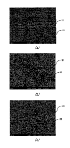
FIG. 1 is SEM photographs of solder alloys: FIG. 1(a) is a cross-section SEM
photography of the solder alloy of Comparative Example 1; FIG. 1(b) is the
cross-
7
Date Re9ue/Date Received 2020-09-03
CA 03093091 2020-09-03
section SEM photography of the solder alloy of Comparative Example 2; and FIG.
1(c) is the cross-section SEM photography of the solder alloy of Example 2.
[DESCRIPTION of EMBODIMETNS]
[0026]
The present invention is described in more detail below. In this description,
"%" with respect to a solder alloy composition is "mass%" unless otherwise
specified.
[0027]
1. Alloy composition of solder alloy
(1) Bi: 35 to 68%
Bi is an element required to suppress generation of the fusion failure by
lowering the melting point of the solder alloy and to exhibit excellent heat-
cycle
resistance. Since the melting point of a Sn-Bi eutectic alloy is as low as 139
C,
Bi is able to lower the melting point of the solder alloy and suppress the
fusion
failure. In addition, it is known that the solder alloy containing a
predetermined
amount of Bi exhibits superplasticity, and exhibits excellent ductility.
Therefore,
the solder alloy containing the predetermined amount of Bi is excellent in the
ductility and the heat-cycle resistance.
[0028]
If the content of Bi is less than 35%, the fusion failure may occur due to an
increase in the melting point, and the tensile strength and the heat-cycle
resistance
may deteriorate. The lower limit of the content of Bi is 35% or more,
preferably
45% or more, more preferably 50% or more, and still more preferably 54% or
more.
8
Date Re9ue/Date Received 2020-09-03
CA 03093091 2020-09-03
On the other hand, if the content of Bi exceeds 68%, the fusion failure may
occur
due to the increase in the melting point. Further, due to a precipitation of a
large
amount of the hard, brittle and coarse Bi phase, the solder alloy itself
becomes hard
and the ductility deteriorates. An upper limit of the content of Bi is 68% or
less,
preferably 65% or less, more preferably 63% or less, and still more preferably
58%
or less.
[0029]
(2) In: 0.5 to 3.0%
In is an element required for lowering the melting point of the solder alloy,
making the alloy organization fine, and improving excellent ductility, impact
resistance and heat-cycle resistance. In is the solid solution strengthening
element,
and since In is dissolvable in Sn and Bi to form crystal core, the alloy
organization
becomes uniform and fine and the ductility is improved. In addition, the
solder
alloy containing a predetermined amount of In is excellent in the heat-cycle
resistance. When the content of In is within the range mentioned above, phase
transformation between f3Sn and ySn is suppressed during the heat cycling and
a
higher heat-cycle resistance can be obtained.
[0030]
If the content of In is less than 0.5%, the effects mentioned above cannot be
exhibited. In addition, the fusion failure may occur due to the increase in
the
melting point. The lower limit of the content of In is 0.5% or more,
preferably
0.7% or more, more preferably 1.0% or more. On the other hand, when the
content
of In exceeds 3.0%, since a large amount of the intermetallic compound is
9
Date Re9ue/Date Received 2020-09-03
CA 03093091 2020-09-03
precipitated, the tensile strength deteriorates. Further, since f3Sn is
transformed
into 7Sn during a heat cycle test, volume of the solder alloy is changed and
the
heat-cycle resistance deteriorates. The upper limit of the content of In is
3.0% or
less, preferably 2.5% or less, more preferably 2.2% or less, and particularly
preferably 2.0% or less.
[0031]
(3) Pd: 0.01 to 0.10%
Pd is an element required to improve the tensile strength while maintaining
the
ductility of the solder alloy. If the content of Pd is within a predetermined
range
in a Sn-Bi-In-Pd solder alloy where the contents of Bi and In are within the
ranges
mentioned above, it is possible to suppress that the solder alloy becomes a
compound containing coarse Sn and Pd. Detailed reasons of this are unknown,
but are guessed as follows.
[0032]
Because of dragging effect in which diffusion speed of Sn becomes slow due
to solid solution of In to Sn and Bi, formation of the compound containing
coarse
Sn and Pd is suppressed. Therefore, when Pd is contained in the predetermined
amount in Sn-Bi-In-Pd solder alloy where the contents of Bi and In are within
the
ranges mentioned above, it is possible to suppress the precipitation of the
compound containing coarse Sn and Pd, and thus the alloy organization becomes
fine. In detail, the Bi phase being a brittle phase becomes finer than a Sn
phase
being a stress-relaxation phase, and a particularly excellent ductility is
exhibited.
Such the fine alloy organization is obtained only in a alloy composition in
which
Date Re9ue/Date Received 2020-09-03
CA 03093091 2020-09-03
Sn contains Bi and In at the same time and also contains Pd. Further, in the
alloy
composition containing Pd, since a large number of solidified core of Pd are
generated, growing of the Sn phase precipitated around each of the cores is
suppressed, and the entire structure becomes fine. As a result, the mechanical
strength and the impact resistance are improved by the precipitation of a
compound
containing fine Sn and Pd.
[0033]
Tithe content of Pd is less than 0.01%, the effects mentioned above cannot be
exhibited. The lower limit of the content of Pd is 0.01% or more. On the other
hand, if the content of Pd exceeds 0.10%, the compound containing coarse Sn
and
Pd precipitates. In addition, the fusion failure may occur due to the increase
in
the melting point. The upper limit of the content of Pd is 0.10% or less,
preferably
0.08% or less, more preferably 0.05% or less, and particularly preferably
0.03% or
less.
[0034]
(5) 0.1% or less of at least one of Co, Ti, Al and/or Mn in total
These elements are optional elements which may be contained as long as they
do not hinder the effects mentioned above. From a viewpoint of maintaining the
mechanical properties, the impact resistance and the heat-cycle resistance
while
suppressing the formation of compounds and also keeping the miniaturization of
the alloy organization, the content of these elements is preferably 0.1% or
less.
[0035]
(6) 0.1 mass% or less of at least one of P. Ge and Ga
11
Date Re9ue/Date Received 2020-09-03
CA 03093091 2020-09-03
These elements are optional elements capable of suppressing oxidation of Sn
and improving the wettability. If the content of these elements does not
exceed
0.1%, the fluidity of the solder alloy on a solder surface is not impaired.
The total
of the content of these elements is more preferably 0.003 to 0.01%. Although
the
content of each element is not particularly limited, the content of P is
preferably
0.002 to 0.005%, the content of Ge is preferably 0.002 to 0.006%, and the
content
of Ga is preferably 0.002 to 0.02% in order to sufficiently express the
effects
mentioned above.
[0036]
(7) Balance: Sn
A balance of the solder alloy according to the present invention is Sn. In
addition to the elements mentioned above, an unavoidable impurity may be
contained. Even when the unavoidable impurity is contained, the effects
mentioned above are not affected. As will be described later, even if an
element
which is not contained in the present invention is contained as the
unavoidable
impurity, the effects mentioned above are not affected.
[0037]
(8) Zr, Ni, Al and Ag, Fe, Ca, Pt, Mg and Sb
It is desirable that the solder alloy according to the present invention does
not
contain these elements. Simultaneous addition of Al and Ag, Zr or Ni forms
coarse compounds which prevent the formation of a uniform and fine alloy
organization. Fe, Ca, Pt or Mg promotes the coarsening of the alloy
organization.
When Sb is combined with In, the ductility is remarkably lowered. Note that
when
12
Date Re9ue/Date Received 2020-09-03
CA 03093091 2020-09-03
these elements are contained as the unavoidable impurities, the effects
mentioned
above are not affected.
[0038]
2. Solder paste
The solder alloy according to the present invention may be used as a solder
paste. The solder paste is a pasty form of solder alloy powder mixed with a
small
amount of fluxes. The solder alloy according to the present invention may be
used
as a solder paste for mounting an electronic component on a printed circuit
board
by a reflow soldering method. The flux used in the solder paste may be either
a
water-soluble flux or a non-water-soluble flux. Typically, a rosin-based flux
is
used which is a rosin-based, water insoluble flux.
[0039]
The solder paste according to the present invention may be applied to an
electrode on a board side to be used for bonding to a Sn-Ag-Cu solder ball on
a
BGA side.
[0040]
3. Solder ball
The solder alloy according to the present invention may be used as a solder
ball. The solder ball according to the present invention is used for forming a
bump
on the electrode of a semiconductor package such as BGA (Ball Grid Arrays), or
substrates. The diameter of the solder ball according to the present invention
is
preferably 1 to 1000p,m. The solder ball can be manufactured by a common
solder
ball manufacturing method.
13
Date Re9ue/Date Received 2020-09-03
CA 03093091 2020-09-03
[0041]
4. Resin flux-cored solder
The solder alloy according to the present invention is suitably used in a
resin
flux-cored solder where flux is previously contained in the solder. It may
also be
used in a form of wire solder from the viewpoint of supplying the solder to a
soldering iron. Furthermore, it may be applied to an incoming wire solder in
which the flux is sealed to the wire solder. The surface of each solder may be
coated with the flux. In addition, the flux may be coated on the surface of
the
solder in which the flux is not contained.
[0042]
The content of the flux in the solder is, for example, 1 to 10 mass%, and the
content of the rosin in the flux is 70 to 95%. Generally, the rosin is an
organic
compound and contains carbon and oxygen, and therefore, the rosin used in the
present invention is not limited by a terminal functional group or the like.
[0043]
5. Solder joint
A solder joint according to the present invention connects an IC chip and a
substrate (an interposer) in a semiconductor package, or connects the
semiconductor package and a printed circuit board. That is, the solder joint
according to the present invention is referred to as a connecting portion of
the
electrode, and is able to form by using a common soldering condition.
[0044]
14
Date Re9ue/Date Received 2020-09-03
CA 03093091 2020-09-03
5. Other
In addition to the above, the solder alloy according to the present invention
may be used as a preform solder, a solder wire and the like.
[0045]
A manufacturing method of the solder alloy according to the present invention
may be carried out in accordance with a conventional method. A bonding method
using the solder alloy according to the present invention may be carried out
in
accordance with a conventional method by using a reflow method, for example.
When the flow soldering is carried out, the melting point of the solder alloy
may
be approximately 20 C higher than a liquidus temperature. Further, when
bonding
is carried out by the solder alloy according to the present invention, the
alloy
organization may be finer by considering cooling speed during the
solidification.
For example, the solder joint is cooled at the cooling speed of 2 to 3 C/s or
more.
The other bonding conditions may be appropriately adjusted in accordance with
the alloy composition of the solder alloy.
[0046]
The solder alloy according to the present invention can produce a low a-ray
alloy by using a low a-ray material as its raw material. Such the low a-ray
alloy
can suppress soft errors when used to form solder bumps around memories.
Examples
[0047]
Solder alloys were prepared, each of which consists of alloy composition
shown in Table 1, to observe alloy organization and measure the melting point
Date Re9ue/Date Received 2020-09-03
CA 03093091 2020-09-03
(liquidus temperature), and to evaluate the tensile strength, the ductility,
the impact
resistance and the heat-cycle resistance.
[0048]
= Observing alloy organization
Each solder alloy consisting of each alloy composition shown in Table 1 was
cast into a predetermined mold, and the obtained solder alloy was molded with
a
resin and polished, and a portion where the solder alloy was polished by about
half
was photographed with a FE-SEM at 1000-fold magnification.
[0049]
= Liquidus temperature
Each solder alloy shown in Table 1 was prepared and the liquidus temperature
of the solder alloys were measured. The liquidus temperature was measured by a
DSC-based method similar to the DSC-based method for measuring the solidus
temperature shown in JIS Z 3198-1. When the liquidus temperature was 170 C or
less, it was evaluated as "T", and when it exceeded 170 C, it was evaluated as
"F".
[0050]
= Tensile strength and ductility
The tensile strength was measured according to JISZ3198-2. For each solder
alloy listed in Table 1, a test piece having a gauge length of 30mm and a
diameter
of 8mm was produced by casting into a mold. The produced test piece was pulled
at a stroke of 6mm/min at room temperature by a Type5966 manufactured by
Instron Corporation, and the tensile strength was measured. Using the same
test
piece, the test piece was pulled at a stroke of 0.6mm/min at room temperature
by
16
Date Re9ue/Date Received 2020-09-03
CA 03093091 2020-09-03
the Type5966 manufactured by Instron Corporation, and the elongation (the
ductility) when the test piece was broken was measured. In the present
example,
when the tensile strength was 70MPa or more, it was evaluated as "T", and when
the tensile strength was less than 70MPa, it was evaluated as "F". When the
elongation (the ductility) was 120% or more, it was judged to be practically
satisfactory and evaluated as "T". When the elongation was less than 120%, it
was evaluated as "F".
[0051]
= Impact resistance
Each solder alloy listed in Table 1 was atomized to be a solder powder. A
solder paste of the respective solder alloy was prepared by mixing with the
soldering flux made of the pine resin, the solvent, the activator, the
thixotropic
agent, the organic acid or the like. The solder paste was printed on the
printed
circuit board (material: FR-4) having the thickness of 0.8mm with the metal
mask
having the thickness of 120p.m. and 10 BGA components were mounted with the
mounter, and reflow soldering was performed at the maximum temperature of
190 C and the holding time of 60 seconds to produce the test substrate.
[0052]
Next, both ends of the test substrate were fixed to a pedestal with bolts so
that
the BGA component faces the pedestal. In this condition, an impact of 1500G
was
applied in accordance with the JEDEC standard to evaluate the impact
resistance.
Thereafter, a resistance value was measured. When the resistance value was
less
than 1.5 times from an initial resistance value, it was evaluated as "T", and
when
17
Date Re9ue/Date Received 2020-09-03
CA 03093091 2020-09-03
the resistance value was 1.5 times or more, it was evaluated as "F".
[0053]
= Heat-cycle resistance
Each solder alloy listed in Table 1 was atomized to be a solder powder. A
solder paste of the respective solder alloy was prepared by mixing with a
soldering
flux made of a pine resin, a solvent, an activator, a thixotropic agent, an
organic
acid or the like. The solder paste was printed on a printed circuit board
(material:
FR-4) having a thickness of 0.8mm with a metal mask having a thickness of 100
pm,
and 15 BGA components were mounted with a mounter, and reflow soldering was
performed at a maximum temperature of 190 C and a holding time of 60 seconds
to produce a test substrate.
[0054]
The test substrates soldering with the respective solder alloy were placed in
a
heat-cycle test device set to a condition of low temperature ¨40 C, high
temperature +100 C, and the holding time of 10 minutes, and number of cycles
at
which the resistance value of at least one BGA component exceeded 15S2 was
determined from an initial resistance value of 3 to 5. When the cycles were
1700
or more, it was evaluated as "T" and when the cycles were less than 1700, it
was
evaluated as "F".
[0055]
The evaluation results are shown in Table 1.
[0056]
[Table 1]
18
Date Re9ue/Date Received 2020-09-03
0
sv
FO.
X
CD
C
CD
0 ALLOY COMPOSITION (mass%)
LIQUIDUS
TS
DUCTILITY IMPACT HEAT CYCLE
sv
TEMPERATURE
RESISTANCE RESISTANCE
CDSn B1 In
Pd Co T A Mn P Ge Ga Sb Zr NI AI-1Ag Fe Ca Pt Mg
X
CD 1 BAL 35 2.0 0.03
T T T T T
0
CD 2 BAL 58 2.0 0.03
T T T T T
CD
3 BAL 65 2.0 0.03 T T T T T
0-
IV 4 BAL 58 1.0 0.03
T T T T T
0
IV 5 BAL 40 1.0 0.04
T T T T T
9
0 6 BAL 65 1.0 0.05
T T T T T
9
o
7 BAL 58 3.0 0.03 T T T T T
4.,
8 BAL 58 3.0 0.08 T T T T T
9 BAL 58 2.0 0.1 T T T T T
O
10 BAL 58 2.0 0.01 T T T T T
w
-J
a. 11 BAL 58 2.0 0.03 0.1 T T T T T
2
< 12 BAL 58 2.0 0.03
- 0.1 T T T T T
x
w
13 BAL 58 2.0 0.03 - - 0.1 T
T T T T P
14 BAL 58 2.0 0.03 - - - 0.1 T
T T T T o
w
o
15 BAL 58 2.0 0.03 - - - - 0.003
T T T T T ,o
w
o
16 BAL 58 2.0 0.03 - - - - 0.05
T T T T T 0
r
17 BAL 58 2.0 0.03 0.1 T T T
T T 6,
o
6, r-+
18 BAL 58 2.0 0.03 0.01 T T T
T T 0
1
19 BAL 58 2.0 0.03 0.005 T T T
T T o,o
20 BAL 58 2.0 0.03 0.1 T T T T T
0
w
21 BAL 58 2.0 0.03 0.005 T T T T T
22 BAL 58 2.0 0.03 0.01 T T T T T
1 BAL 58 _ ------------------------------ _
T F F F F
2 BAL 58 0.03
T T F
3 BAL 58 2.0 _ -------------------------------- T F T F T
4 BAL 30 2.0 0.03 F F T - -
0
w
5 BAL 75 2.0 0.03 F T F - -
....]
& 6 BAL 58 B4 0.03 F T F - -
<
x 7 BAL 58 4.0 0.03 F T - -
w
- T
Lo 8 BAL 58 2.0 0.2 - F T F - -
>
17- 9 BAL 58 2.0 0.03 0.5 T T F - -
<
cc
<
10 BAL 58 2.0 0.03 4]. ------T F F
a-
11
h
2 BAL 58 2.0 0.03
T F F - -
O I
o
12 BAL 58 2.0 0.03 T F F - -
13 BAL 58 2.0 0.03 T F F - -
14 BAL 58 2.0 0.03 0.1 - T F F - -
15 BAL 58 2.0 0.03 0.1 - T F F - -
16 BAL 58 2.0 0.01 0.1 T F F - -
UNDERLINE MEANS THAT VALUE IS OUTSIDE SCOPE OF PRESENT INVENTION
CA 03093091 2020-09-03
[0057]
As shown in Table 1, Examples 1 to 22 were found to be superior in the tensile
strength, the ductility, and the impact resistance. Further, it was found that
the
generation of the fusion failure was suppressed because the liquidus
temperature
was low, and the coarsening of the alloy organization was suppressed even
after
the heat cycling because the alloy organization was fine, and thus the heat-
cycle
resistance was excellent.
[0058]
On the other hand, since Comparative Example 1 did not contain In and Pd, the
alloy organization did not become fine and was inferior in the tensile
strength, the
ductility, the impact resistance and the heat-cycle resistance. The mechanical
strength of Comparative Example 2 was improved over that of Comparative
Example 1 by the precipitation of a compound of Sn and Pd because it contained
Pd, but the ductility was inferior because it did not contain In. Since the
ductility
of Comparative Example 2 was inferior, the heat-cycle resistance or the impact
resistance were not evaluated. Comparative Example 3 was inferior in the
tensile
strength and the impact resistance because it did not contain Pd.
[0059]
The liquidus temperature of Comparative Example 4 exceeded 170 C because
it contained a small amount of Bi. The liquidus temperature of Comparative
Example 5 exceeded 170 C because it contained a large amount of Bi. The
liquidus temperature of Comparative Example 6 exceeded 170 C because it
contained a small amount of In. The tensile strength of Comparative Example 7
Date Re9ue/Date Received 2020-09-03
CA 03093091 2020-09-03
decreased because it contained a large amount of In. The liquidus temperature
of
Comparative Example 8 exceeded 170 C and the ductility was inferior because it
contained a large amount of Pd. These examples were not evaluated for the heat-
cycle resistance and the impact resistance because at least one of the
liquidus
temperature, the tensile strength and the ductility was inferior.
[0060]
The Comparative Example 9 was inferior in the ductility because In and Sb
coexisted. Therefore, the heat-cycle resistance and the impact resistance were
not
evaluated.
[0061]
The Comparative Examples 10 to 16 were inferior in the ductility and the like
because the alloy organization became coarse.
Therefore, the heat-cycle
resistance and the impact resistance were not evaluated.
[0062]
Observations of the alloy organization of Comparative Examples 1 and 2 and
Example 2 shown in Table 1 are shown. FIG. 1 is SEM photographs of solder
alloys: FIG. 1(a) is a cross-section SEM photography of the solder alloy of
Comparative Example 1; FIG. 1(b) is the cross-section SEM photography of the
solder alloy of Comparative Example 2; and FIG. 1(c) is the SEM photography of
the solder alloy of Example 2. In FIGS. 1(a) to 1(c), white portions
correspond to
the Bi phase and gray portions correspond to the 13-Sn phase.
[0063]
It was found from FIG. 1(a) that the coarse Bi phase exists because In and Pd
21
Date Re9ue/Date Received 2020-09-03
CA 03093091 2020-09-03
are not contained in Comparative Example 1. It was found from FIG. 1(b) that
the alloy organization of Comparative Example 2 was fine in comparison to FIG.
1 (a) because it contained In, whereas it was not sufficiently fine to obtain
desired
characteristics. It was found from FIG. 1(c) from Example 2 that the alloy
organization of Example 2 was finest because it contained In and Pd. In
particular,
it was found that miniaturization of the Bi phase being the brittle phase was
remarkable. In each of the other Examples, it was observed that the alloy
organization was as fine as shown in FIG. 1(c).
[0064]
As mentioned above, the Sn-Bi-In-Pd solder alloy exhibits excellent tensile
strength, ductility, and impact resistance, and heat-cycle resistance because
of its
fine organization.
[Reference Signs List]
[0065]
11, 21, 31 Bi phase
12, 22, 32 Sn phase
22
Date Re9ue/Date Received 2020-09-03