Note: Descriptions are shown in the official language in which they were submitted.
CA 03094929 2020-09-23
DESCRIPTION
MULTICAST SWITCH
Technical Field
[0001] The present invention relates to an optical switch, and more
specifically, relates
to a multicast switch usable in an optical communications system.
Background Art
[0002] A reconfigurable optical add/drop multiplexer (ROADM) is an essential
device
for optical network construction since it can arbitrarily select a path of an
optical
wavelength multiplex signal in an optical fiber transmission channel for each
wavelength
without converting the signal into an electrical signal. A ROADM requires an
optical
switch that freely allocates a wavelength and an input/output port.
[0003] A ROADM generally uses a multicast switch (MC S) obtained by combining
an
optical switch with an optical splitter (optical coupler), which is an optical
device smaller
than a wavelength selection switch and a matrix optical switch (see PTL 1 for
example).
The use of an MCS has the advantage of realizing a small and economical ROADM.
In
the future, the number of wavelengths is expected to increase and an MCS needs
to be
further downsized.
[0004] As a basic optical switch configuration in a ROADM using an MCS, there
is a
Mach-Zehnder interferometer 2x2 optical switch (MZI optical switch) using
quartz
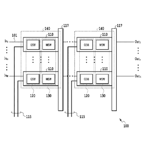
waveguides. An MZI optical switch can change a path through which an optical
signal
passes by providing thermooptic phase shifters (thin-film heaters) near two
arm
waveguides and controlling activation/deactivation of the thin-film heaters.
[0005] FIG. 1 is a diagram showing an example of a conventional MZI optical
switch.
The MZI optical switch shown in FIG. 1 comprises input optical waveguides 11 a
and 11b,
thin-film heaters 12a and 12b, directional couplers 13-1 and 13-2, two arm
waveguides
1
CA 03094929 2020-09-23
14a and 14b, leads 15a to 15d as drive electrical wiring for feeding the thin-
film heaters
12a and 12b, and output optical waveguides 16a and 16b. In the case of using
the MZI
optical switch shown in FIG. 1 as a 1 x2 optical switch, one of the input
optical
waveguides 11 a and lib becomes an unconnected waveguide. In the case of using
the
switch as a 2x 1 optical switch, one of the output optical waveguides 16a and
16b becomes
an unconnected waveguide.
[0006] In the MZI optical switch shown in FIG. 1, the two arm waveguides 14a
and 14b
are generally designed to have a half-wave optical path length difference.
Accordingly,
in a case where the thin-film heaters 12a and 12b are not driven (fed) and the
half-wave
optical path length difference between the two arm waveguides 14a and 14b is
not
cancelled, an optical signal path is a bar path (from the input optical
waveguide 11 a to the
output optical waveguide 16a / from the input optical waveguide lib to the
output optical
waveguide 16b). In a case where the thin-film heaters 12a and 12b are driven
and the
half-wave optical path length difference is cancelled by the thermooptic
effect, an optical
signal path is a cross path (from the input optical waveguide 11 a to the
output optical
waveguide 16b / from the input optical waveguide lib to the output optical
waveguide
16a). In a case where the half-wave optical path length difference is not
provided
between the two arm waveguides 14a and 14b, the above operation is reversed in
the MZI
optical switch shown in FIG. 1. That is, activation/deactivation of the MZI
optical
switch can be controlled via activation/deactivation of the thin-film heaters
12a and 12b
by controlling feeding by the leads 15a to 15d.
[0007] Since the MZI has no directivity, the terms "input port" and "output
port" are
used only for the sake of identification and each of them can be used for both
input and
output.
[0008] FIG. 2 is a diagram showing an example of an MCS formed by a
conventional
MCS having four inputs and four outputs (hereinafter referred to as a 4x4 MCS)
using
MZI optical switches. FIG. 2 shows an MCS comprising four input ports Ini to
In4 and
2
CA 03094929 2020-09-23
output ports Outi to 0ut4 each connected to an optical waveguide, 1 x2
splitters SP, gate
switches GSWi , 1 to GSW4,4 that are 1 x2 switches, main switches MSW1,1 to
MSW4,4
that are 2x1 switches, leads 15 for controlling activation/deactivation of GSW
and MSW,
and ground lines 17 for grounding GSW and MSW. As GSW and MSW, MZI optical
switches as shown in FIG. 1 are used. In a conventional MCS, a bend radius of
an
optical waveguide is large. Thus, for downsizing, it has been advantageous to
use the
structure of reducing the longitudinal direction, not the structure of
bending.
Accordingly, there has been a need for an arrangement in which GSW and MSW are
staggered vertically to make up gaps (nested arrangement).
[0009] The 1 x2 splitters SP are asymmetrical splitters and a splitting ratio
is sequentially
set at 3:1, 2:1, and 1:1 from a 1x2 splitter SP in the first line onward. This
is to prevent
a difference in optical output between the output ports.
[0010] The 4x4 MCS shown in FIG. 2 has a pair of GSW and MSW whose
activation/deactivation is controlled in a case where an optical signal input
to a specific
input port is output from a specific output port, and this pair constitutes an
optical switch
unit SU. For example, an optical signal input to the input port Ini can be
output from
the output port Outi by controlling activation/deactivation of GSWi , 1 and
MSW1, 1 .
The optical switch unit SU can be classified into a configuration of SUa shown
in FIG. 3
and a configuration of SUb shown in FIG. 4.
[0011] FIG. 3 is a diagram showing a configuration of conventional SUa. FIG. 3
shows SUa including a 1x2 splitter SP, GSW, and MSW. As shown in FIG. 3, SUa
is a
1 x2 switch combined with a splitter having first and second input ends a and
b and first
and second output ends c and d.
[0012] GSW and MSW are connected to different leads 15 and ground lines 17 and
each
have one output end connected to a termination waveguide e. GSW and MSW have
the
function of a crossbar switch, that is, each of them enters a bar state
(connected to the
termination waveguide e) in an inactive state in which no voltage is applied
and enters a
3
CA 03094929 2020-09-23
cross state (transmission state) in an active state in which voltage is
applied via the lead
15.
[0013] As shown in FIG. 3, a first optical signal input from the first input
end a of SUa
is branched into two by the 1 x2 splitter SP. One branch of the first optical
signal is
coupled to the first output end c of SUa and the other branch of the first
optical signal is
coupled to the input end of GSW. GSW enters the bar state and outputs the
first optical
signal to the termination waveguide e in the inactive state, and enters the
cross state and
outputs the optical signal to MSW in the active state.
[0014] MSW receives input of the first optical signal from the first input end
a of SUa
via GSW and input of a second optical signal from the second input end b of
SUa. MSW
enters the bar state and outputs the second optical signal to the second
output end d of
SUa in the inactive state, and enters the cross state, outputs the second
optical signal to
the termination waveguide e, and outputs the first optical signal to the
second output end
d of SUa in the active state.
[0015] FIG. 4 is a diagram showing a configuration of conventional SUb. FIG. 4
shows SUb including a gate switch GSW, a main switch MSW, and leads 15. As
shown
in FIG. 4, SUb is a 2x1 switch having first and second input ends a and b and
an output
end d. GSW and MSW are connected to different leads 15 and ground lines 17.
[0016] As shown in FIG. 4, a first optical signal input from the first input
end a of SUb
is coupled to the input end of GSW. GSW enters the bar state and outputs the
first optical
signal to the termination waveguide e in the inactive state, and enters the
cross state and
outputs the optical signal to MSW in the active state.
[0017] MSW receives input of the first optical signal from the first input end
a of SUb
via GSW and input of the second optical signal from the second input end b of
SUb.
MSW enters the bar state and outputs the second optical signal to the output
end d of SUb
in the inactive state, and enters the cross state, outputs the second optical
signal to the
termination waveguide e, and outputs the first optical signal to the output
end d of SUb
4
CA 03094929 2020-09-23
in the active state.
Citation List
Patent Literature
[0018]
PTL 1: Japanese Patent No. 5913139
Summary of Invention
Technical Problem
[0019] In the case of the conventional 4x4 MCS shown in FIG. 2, since it is
necessary
to connect GSW and MSW to different leads 15, the necessary number of leads 15
is
(4x4)x2 = 32. In the conventional 4x4 MCS shown in FIG. 2, the leading
direction of
leads 15 is a direction perpendicular to the direction of input/output of
signal light because
of necessity to lay out the leads 15 without any intersection on the substrate
and ease of
work/process. Accordingly, there has been a problem that 32 leads 15 are
arrayed and a
large area is occupied by the 32 leads 15. Further, in the case of an MxN MCS,
since
the necessary number of leads is (mx-N) x2, there has been a problem that the
number of
leads increases with the number of input/output ports and their footprint
becomes larger.
[0020] In addition, in the conventional 4x4 MCS shown in FIG. 2, a ground line
17 is
provided for each array of MZI optical switches connected to the leads 15.
Thus, the
footprint of electrical wiring further becomes larger by including the ground
lines 17.
[0021] On the other hand, a reduction in the line width of the leads 15 or the
interval
between the leads 15 is considered as a measure to suppress an increase in
footprint of
electrical wiring. However, in consideration of the amount of current
necessary for
driving the thin-film heaters 12, there is a limit due to a high possibility
of a break or short
circuit caused by heater driving current and it is difficult to further reduce
the line width
or interval.
[0022] As described above, there is a problem that as the scale of an optical
circuit and the
number of channels are increased, the ratio of electrical wiring such as leads
15 and ground
lines 17 to the substrate is also increased, which becomes an obstacle to
downsizing of an
optical switch
[0023] The present invention has been accomplished in view of the above
problem. The
object of the present invention is to provide a small multicast switch with a
reduced number
of leads.
Solution to Problem
[0024] A multicast switch according to an aspect of the present invention is
formed on a
high-refractive-index waveguide substrate, comprising; M input ports to which
optical
signals are input, the input ports being associated with different numbers out
of first numbers
1, M;
N output ports from which the optical signals are output, the output ports
being
associated with different numbers out of second numbers 1, N,
MxN optical switch units
associated with different pairs of numbers [m, n], where m is an integer
satisfying 1 < m <
M and corresponds to the first numbers and n is an integer satisfying 1 < n <
N and
corresponds to the second number, optical waveguides optically connecting the
M input ports,
the MxN optical switch units; and the N output ports, and leads connected to
the MxN optical
switch units, respectively, to control activation/deactivation of the optical
switch units,
wherein by activating one optical switch unit of the MxN optical switch units,
an optical
signal input to the input port associated with the first number associated
with the activated
optical switch unit is output from the output port associated with the second
number
associated with the activated optical switch unit, the MxN optical switch
units include at least
a gate switch that is a 1 xl switch and a main switch that is a 2x1 switch
provided in a
subsequent stage of the gate switch, and in each of the optical switch units,
the gate switch
and the main switch are connected to a common lead. The optical switch units
include a first
optical switch unit comprising a 1 x2 splitter in a preceding stage and a
second optical switch
6
Date Recue/Date Received 2022-02-02
unit not comprising the 1x2 splitter, and optical switch units connected to
the output ports
are second optical switch units.
6a
Date Recue/Date Received 2022-02-02
CA 03094929 2020-09-23
Advantageous Effects of Invention
[0025] According to the multicast switch of the present invention, downsizing
of the
MCS can be realized.
Brief Description of Drawings
[0026]
[FIG. 1] FIG. 1 is a diagram showing an example of a conventional MZI optical
switch;
[FIG. 2] FIG. 2 is a diagram showing an example of an MCS using conventional
4x4 MZI optical switches;
[FIG. 3] FIG. 3 is a diagram showing an example of a configuration of
conventional SU;
[FIG. 4] FIG. 4 is a diagram showing an example of a configuration of
conventional SU;
[FIG. 5] FIG. 5 is a diagram for explaining the operation of a 4><4 MCS;
[FIG. 6] FIG. 6 is a diagram for explaining the operation of a 4x4 MCS having
a different configuration;
[FIG. 7] FIG. 7 is a diagram showing a simplified example of a configuration
of
an MxN MCS according to a first embodiment of the present invention;
[FIG. 8] FIG. 8 is a diagram showing an example of a configuration of SU
according to the first embodiment of the present invention;
[FIG. 9] FIG. 9 is a diagram showing an example of a configuration of SU
according to the first embodiment of the present invention;
[FIG. 10] FIG. 10 is a diagram showing another example of a
configuration of SU according to the first embodiment of the present
invention;
[FIG. 11] FIG. 11 is a diagram showing another example of a
configuration of SU according to the first embodiment of the present
invention;
7
CA 03094929 2020-09-23
[FIG. 12] FIG. 12 is a diagram showing yet another example of a
configuration of SU according to the first embodiment of the present
invention;
[FIG. 13] FIG. 13 is a diagram showing yet another example of a
configuration of SU according to the first embodiment of the present
invention;
[FIG. 14] FIG. 14 is a diagram showing further another example of a
configuration of SU according to the first embodiment of the present
invention;
[FIG. 15] FIG. 15 is a diagram showing further another example of a
configuration of SU according to the first embodiment of the present
invention;
[FIG. 16] FIG. 16 is a diagram showing a simplified example of an
MxN
MCS according to a second embodiment of the present invention;
[FIG. 17] FIG. 17 is a diagram showing an example of a configuration
of
a 4x4 MCS according to a third embodiment of the present invention;
[FIG. 18] FIG. 18 is a diagram showing a simplified example of a
configuration of a 4x4 MCS according to the third embodiment of the present
invention.
[FIG. 19] FIG. 19 is a diagram showing an example of a 4>4 MCS
according to a fourth embodiment of the present invention; and
[FIG. 20] FIG. 20 is a diagram showing an example of a configuration
of
an 8 x 16 MCS according to a fifth embodiment of the present invention.
Description of Embodiments
[0027] As a result of careful consideration of an operation state of an
optical switch, the
inventors have found out that active MZI optical switches are not totally
randomly present
on an M xN matrix but are present under a certain restriction. That is, the
inventors have
found out that in a case where either one of GSW and MSW in SU is activated,
the other
is simultaneously activated, and similarly, in a case where either one is
deactivated, the
other is simultaneously deactivated. In view of such a restriction condition,
if leads of
GSW and MSW in SU can be shared and concentrated, the footprint of the leads
can be
8
CA 03094929 2020-09-23
reduced.
[0028] FIG. 5 is a diagram for explaining the operation of a 4 x 4 MCS. In
FIG. 5,
illustration of wiring is omitted. FIG. 5 shows 16 optical switch units SU 1,1
to SU 4, 4 =
In the 4 x 4 MCS, SU 3,1, SU 4,2, SU 1,3, and SU 2,4 connected to output ports
Outi to
0ut4, respectively, are SUb and the other optical switch units are SUa. An
optical signal
input from an optical switch unit SUa passes through two optical switch units
SUa and is
then output from an output side optical switch unit SUb.
[0029] In a case where voltage is applied to none of the optical switch units
SU, since
all optical signals from input ports Ini to In4 are connected to the
termination waveguides
e, the signals are not output to the output ports Outi to 0ut4. For example,
since an
optical signal from the input port Ini is connected to the termination
waveguide e at SU
1,3, the signal is not output to the output ports Out' to 0ut4 . Similarly,
since the input
ports In2 to In4 are connected to the termination waveguides e at SU 2,4, SU
3, 1, and SU
4, 2 , respectively, signals are not output to the output ports Outi to 0ut4
[0030] For example, an optical signal from the input port In2 can be output to
the output
port 0ut3 by applying voltage to SU 2, 3 . At this time, the optical signal
from the input
port In2 passes through SU 2,2 and SU 2, 1 in the bar state, active SU 2, 3 in
cross state,
and SU 1,3 in the bar state, and is then output from the output port 0ut3 .
[0031] In a case where the setting of the function of SU is reversed such that
a switch
enters the cross state (connected to the termination waveguide) in a normal
state in which
no voltage is applied and enters the bar state (transmission state) in a
voltage-applied state,
the layout is as shown in FIG. 6.
[0032] In the case of an MxN MCS, SU includes Mx (N-1) optical switch units
(SUa)
and M optical switch units (SUb) connected to output ports. An optical signal
input
from In can be output to Outn by controlling activation/deactivation of SUni n
=
[First Embodiment]
[0033] FIG. 7 is a diagram showing a simplified example of a configuration of
an MxN
9
CA 03094929 2020-09-23
MCS 100 (each of M and N is an integer not less than two) of the first
embodiment of the
present invention. FIG. 7 shows the MxN MCS 100 obtained by forming, on a high-
refractive-index waveguide substrate, M input ports Ini to Inm to which
optical signals
are input, N output ports Outi to OutN from which optical signals are output,
MxN optical
switch units SU 110, optical waveguides 101 optically connecting the input
ports Ini to
Inm , SU 110, and output ports Outi to OutN , MxN leads 115 connected to the
respective
optical switch units SU 110 so as to control activation/deactivation of each
SU 110 by
feeding each SU 110, and ground lines 117 for grounding SU 110.
[0034] SU 110 [m, n], the input port In, and the output port Outn are
associated with
one another such that an optical signal input to the input port Inm is output
to the output
port Outn by activating SU 110 [m, n]. Here, m is an integer satisfying 1 < m
< M and
corresponds to the first number relating to the input port, and n is an
integer satisfying 1
< n < N and corresponds to the second number relating to the output port.
[0035] As shown in FIG. 7, the MxN MCS 100 of the first embodiment includes a
plurality of optical switch unit arrays (hereinafter referred to as SU arrays)
140, each of
which includes a plurality of optical switch units SU 110 arrayed vertically
(in parallel
with the leads 115 and ground 117). The ground line 117 is arranged in
parallel with
each SU array 140. The ground line 117 arranged in parallel is connected to
each SU
110 of each SU array 140.
[0036] Each SU 110 includes GSW that is a 1 x 1 switch and MSW that is a 2 x 1
switch
provided in the subsequent stage of GSW. In each SU array 140, a plurality of
gate
switches GSW and a plurality of main switches MSW included in the respective
optical
switch units SU 110 are arrayed vertically to form a GSW array 120 and an MSW
array
130. GSW and MSW included in each SU 110 are connected to the same single
lead.
In the MxN MCS 100 of the first embodiment, the optical switch units SU 110
are arrayed
like vertical and horizontal lines on the high-refractive-index waveguide
substrate and
arranged in a lattice pattern. However, the positions of SU 110 may be shifted
within
CA 03094929 2020-09-23
an allowable range of layout of common electrical wiring such as leads. As
shown in
FIG. 7, the GSW arrays 120 and the MSW arrays 130 are alternately arrayed from
the
input ports to the output ports. The input ports Ini to Inm are connected to
GSW and
the output ports Outi to OutN are connected to MSW.
[0037] FIG. 8 and FIG. 9 are diagrams showing examples of configurations of
SUa and
SUb, respectively, according to the first embodiment of the present invention.
As shown
in FIG. 8 and FIG. 9, in SUa and SUb of the first embodiment, GSW and MSW are
connected in series by a common lead 115 and ground line 117 such that
activation/deactivation of the switches is simultaneously controlled. Wiring
of GSW
and MSW is laid out so as to connect without any intersection. SUa and SUb of
the first
embodiment are identical to SUa and SUb shown in FIG. 3 and FIG. 4 except that
they
are connected by the common lead 115 and ground line 117.
[0038] In the MxN MCS 100 of the first embodiment shown in FIG. 7, among the
MxN
optical switch units SU, optical switch units SU connected to Outi to OutN are
SUb
shown in FIG. 9 and the other optical switch units SU are SUa shown in FIG. 8
(the 1 x2
splitter SP connected in the preceding stage of SUa is omitted for
simplification). In the
embodiments described below, SUa and SUb have the same configurations as SUa
and
SUb shown in FIG. 8 and FIG. 9.
[0039] In the MxN MCS 100 of the first embodiment, by activating one of MxN
optical
switch units SU, an optical signal input to an input port associated with the
first number
associated with activated SU is output from an output port associated with the
second
number associated with activated SU. For example, by activating an optical
switch unit
SU associated with any number [m, n], an optical signal input to an input port
Inn, can be
output from an output port Outn
[0040] FIG. 10 and FIG. 11 are diagrams showing other examples of
configurations of
SUa and SUb, respectively, according to the first embodiment of the present
invention.
As shown in FIG. 10 and FIG. 11, in SUa and SUb, GSW and MSW may be connected
11
CA 03094929 2020-09-23
in parallel by the common lead 115 and ground line 117.
[0041] FIG. 12 and FIG. 13 are diagrams showing yet other examples of
configurations
of SUa and SUb, respectively, according to the first embodiment of the present
invention.
FIG. 12 and FIG. 13 show SUa and SUb each comprising two or more switches GSWi
to GSWN. In the examples shown in FIG. 12 and FIG. 13, a plurality of gate
switches
GSWi to GSWN and a main switch MSW are connected in parallel by the common
lead
115 and ground line 117 such that activation/deactivation of the switches is
simultaneously controlled.
[0042] According to the examples shown in FIG. 12 and FIG. 13, in the case of
two or
more gate switches GSW, noise can be reduced since light leakage in the
inactive
operation of the first switch GSWi can be shut off by the subsequent switch
GSW. In
addition, according to the examples shown in FIG. 12 and FIG. 13, the number
of wiring
can be reduced by N with respect to the number N of gate switches GSW as
compared
with the case of increasing the number of gate switches GSW in the
conventional method
not using a common lead.
[0043] FIG. 14 and FIG. 15 are diagrams showing further other examples of
configurations of SUa and SUb, respectively, according to the first embodiment
of the
present invention. In the examples shown in FIG. 12 and FIG. 13, a plurality
of gate
switches GSWi to GSWN and a main switch MSW are connected in parallel.
However,
the configuration is not limited to this. Like the examples shown in FIG. 14
and FIG.
15, a plurality of gate switches GSWi to GSWN and a main switch MSW may be
connected in series by the common lead 115 and ground line 117.
[0044] According to the MCS of the first embodiment, downsizing of the MCS can
be
realized since the number of leads can be reduced by half as compared with the
conventional configuration by using a common lead for GSW and MSW of each
optical
switch unit.
[Second Embodiment]
12
CA 03094929 2020-09-23
[0045] FIG. 16 is a diagram showing a simplified example of a configuration of
an MxN
MCS 200 according to the second embodiment of the present invention. FIG. 16
shows
the MxN MCS 200 obtained by forming, on a high-refractive-index waveguide
substrate,
M input ports Ini to Inm to which optical signals are input, N output ports
Outi to OutN
from which optical signals are output, MxN optical switch units SU 210,
optical
waveguides 201 optically connecting the input ports Ini to Inm , SU 210, and
output ports
Outi to OutN, MxN leads 215 connected to the respective optical switch units
SU 210 so
as to control activation/deactivation of each SU 210, and ground lines 217 for
grounding
SU 210.
[0046] As shown in FIG. 16, the MxN MCS 200 of the second embodiment includes
a
plurality of SU arrays 240 constituted of SU arrays 2401 to 240,, . Each SU
array 240 is
formed by vertically arraying a plurality of optical switch units SU 210.
[0047] The MxN MCS 200 of the second embodiment comprises a folded waveguide
portion 202 formed by folding an optical waveguide 201 between adjacent SU
arrays 240.
[0048] In the second embodiment, x, which is the number of SU arrays 240, is
an even
number not less than two. Further, in the MxN MCS 200 of the second
embodiment,
two SU arrays 240 are folded and thereby vertically arrayed to form an SU
array 250.
Depending on the position of the folded waveguide portion 202, the SU array
250
comprises at least M+M, M+N, or N+N optical switch units SU 210. Since it is
advantageous to fold near the middle of the SU array 240 for downsizing of the
MCS, it
is preferable to include M+N optical switch units SU 210 in the SU array 250.
In the
case of folding in the middle, the number of SU arrays 250 is x/2.
[0049] Each SU 210 includes GSW and MSW provided in the subsequent stage of
GSW.
Each of the SU arrays 2401 to 240õ has a GSW array 220 and an MSW array 230.
The
GSW arrays 220 and the MSW arrays 230 are alternately arrayed from the input
ports to
the output ports. The input ports Ini to Inm are connected to GSW and the
output ports
Outi to OutN are connected to MSW.
13
CA 03094929 2020-09-23
[0050] In the MxN MCS 200 of the second embodiment, the folded waveguide
portion
202 for converting an optical path 180 is provided between the x/2th SU array
240x/2
and the (x/2)+1th SU array 240( x/2)+1 . Half of the SU arrays 2401 to 240x
are thus
folded, whereby the input ports Ini to Inm and the output ports Outi to OutN
are arranged
on the same side. The folded waveguide portion 202 can be configured to
convert an
optical path 180 by, for example, providing the waveguide with two bent
waveguide
portions for 90 optical path conversion having an arbitrary bend radius.
[0051] Here, on the assumption that k is an integer satisfying 1 < k < x/2, as
shown in
FIG. 16, the output port side is folded, whereby the input port side SU array
2401 and the
output port side SU array 240k, the input port side SU array 2402 and the
output port side
SU array 240x _1, ..., the input port side SU array 240k and the output port
side SU array
240x_ k + 1, ..., and the input port side SU array 240x/2 and the output port
side SU array
240( x/2)+1 are further vertically arrayed to form SU arrays 250. Two SU
arrays 240
are vertically arrayed to form an SU array 250. A single common ground line
217 is
connected to each SU 210 in each SU array 250.
[0052] In the MxN MCS 200 of the second embodiment, in addition to using the
common leads 215, the optical waveguide 201 is folded at the center of the SU
arrays
2401 to 240x , and the single common ground line 217 is used for each SU array
250.
Therefore, according to the MxN MCS 200 of the second embodiment, the number
of
leads can be reduced by half as compared with the conventional technique by
using the
common leads 215. Furthermore, the length of the SU arrays 240 in the array
direction
between the input and output ports is reduced from x to x/2 by the folding
structure, that
is, the length in the array direction can be reduced by about half. Moreover,
the number
of ground lines can be reduced by using the common ground line 217 for an
input port
side SU array and an output port side SU array. As a result, further
downsizing of the
MCS can be realized.
[0053] Here, although the number of SU arrays 240 is an even number in the
second
14
CA 03094929 2020-09-23
embodiment, the folding structure of the second embodiment is also applicable
to the case
where the number of SU arrays 240 is an odd number. In this case, on the
assumption
that the number of SU arrays 240 is y (y is an odd number), it is preferable
to provide the
folded waveguide portion 202 in an optical waveguide between the (y 1)/2th SU
array
240 and the (y 1)/2 }+Ph SU array 240.
[0054] Further, although the second embodiment shows the folding structure in
which
the folded waveguide portion 202 is provided between the x/2' SU array 240x/2
and the
(x/2)+1th SU array 240(x72)+1, the folding structure is not limited to this
and the folded
waveguide portion 202 may be provided between any SU arrays 240. Furthermore,
at
least one pair of an input port side SU array 240 before being folded by the
folding
structure and an output port side SU array 240 after being folded by the
folding structure
forms an SU array 250, and the common ground line 217 can be used in each SU
210 in
the SU array 250. This can bring about the advantageous effects of this
embodiment,
that is, a reduction in length of the SU arrays 240 in the array direction and
a reduction in
number of ground lines.
[Third Embodiment]
[0055] FIG. 17 is a diagram showing a configuration of a 4x4 MCS according to
the
third embodiment of the present invention. FIG. 17 shows a 4x4 MCS 300
obtained by
forming, on a high-refractive-index waveguide substrate, four input ports Ini
to In4, four
output ports Outi to 0ut4, 16 optical switch units SU 310, optical waveguides
301
optically connecting the input ports Ini to In4, SU 310, and output ports Outi
to Outi,
16 leads 315 connected to the respective optical switch units SU 310, and four
ground
lines 317.
[0056] As shown in FIG. 17, the 4x4 MCS 300 of the third embodiment includes
four
SU arrays 3401 to 3404 each including four vertically arrayed optical switch
units SU
310. Each SU 310 includes GSW and MSW provided in the subsequent stage of GSW.
Each of the SU arrays 3401 to 3404 has a GSW array 320 and an MSW array 330.
The
CA 03094929 2020-09-23
GSW arrays 320 and the MSW arrays 330 are alternately arrayed from the input
ports to
the output ports. The input ports Ini to In4 are connected to GSW and the
output ports
Outi to 0ut4 are connected to MSW. A common lead 315 is connected to GSW and
MSW of each SU 310.
[0057] Each SU 310 in the first to third SU arrays 3401 to 3403 is equipped
with a 1 x2
splitter SP in the preceding stage of GSW. The 1 x2 splitter SP is an
asymmetrical
splitter and a splitting ratio is sequentially set at 3:1, 2:1, and 1:1 in the
order of the first
SU array 3401, the second array, and the third SU array 3403.
[0058] FIG. 18 is a diagram showing a simplified example of a configuration of
a 4x4
MCS 300 according to the third embodiment of the present embodiment. FIG. 18
shows
16 optical switch units SU 1,1 to SU 4,4. In the 4 x 4 MCS 300 of the third
embodiment,
SU 4,1, SU 2,2, SU 3,3, and SU 1,4 connected to the respective output ports
Outi to Out4
are SUb and the other optical switch units are SUa.
[0059] In the 4x4 MCS 300 of the third embodiment, for example, an optical
signal
from the input port In2 can be output to the output port 0ut3 by applying
voltage to SU
2,3. At this time, the optical signal from the input port In2 passes through
SU 2,4 in the
bar state, active SU 2,3 in the cross state, and SU 4,3 and SU 3.3 in the bar
state, and is
then output from the output port 0ut3.
[0060] According to the 4x4 MCS 300 of the third embodiment, the number of
leads
can be reduced by half as compared with the configuration of the conventional
4><4 MCS
shown in FIG. 2. Therefore, the footprint of leads can be reduced and
downsizing of the
MCS can be realized.
[Fourth Embodiment]
[0061] FIG. 19 is a diagram showing a configuration of a 4x4 MCS according to
the
fourth embodiment of the present invention. FIG. 19 shows a 4x4 MCS 400
obtained
by forming, on a high-refractive-index waveguide substrate, four input ports
Ini to 1n4,
four output ports Outi to 0ut4, 16 optical switch units SU 410, optical
waveguides 401
16
CA 03094929 2020-09-23
optically connecting the input ports Ini to In4, SU 410, and output ports Outi
to 0ut4,
16 leads 415 connected to the respective optical switch units SU 410, and two
ground
lines 417.
[0062] As shown in FIG. 19, the 4x4 MCS 400 of the fourth embodiment includes
four
SU arrays 4401 to 4404, each SU array 440 including four optical switch units
SU 410.
The SU arrays 4401 to 4404 have a folded waveguide portion 402 in an optical
waveguide
401 between the SU arrays 4402 and 4403 to form a U-shaped array. Since the
4x4
MCS 400 of the fourth embodiment has the folded waveguide portion 402 between
the
SU arrays 4402 and 4403, which correspond to the center of the SU arrays 4401
to 4404,
two SU arrays 440 are vertically arrayed, with the result that two SU arrays
450 are
formed.
[0063] Each SU 410 includes GSW and MSW provided in the subsequent stage of
GSW.
Each of the SU arrays 4401 to 4404 has a GSW array 420 and an MSW array 430.
The
GSW arrays 420 and the MSW arrays 430 are alternately arrayed from the input
ports to
the output ports. The input ports Ini to In4 are connected to GSW and the
output ports
Outi to 0ut4 are connected to MSW.
[0064] Further, each SU 410 in the SU arrays 4401 to 4403 is equipped with a
1x2
splitter SP in the preceding stage of GSW. The 1 x2 splitter SP is an
asymmetrical
splitter and a splitting ratio is sequentially set at 3:1, 2:1, and 1:1 in the
order of the first
SU array 4401, the SU array 4402, and the SU array 4403.
[0065] In the 4x4 MCS 400 of the fourth embodiment, the folded waveguide
portion
402 is provided in an optical waveguide 401 connecting the SU array 4402 and
SU array
4403. The optical waveguide 401 is thus folded between the second SU array
4402 and
the third SU array 4403, whereby the input ports Ini to In4 and the output
ports Outi to
0ut4 are arranged on the same side.
[0066] As shown in FIG. 19, the input port side SU array 4401 and the output
port side
SU array 4404, and the input port side SU array 4402 and the output port side
SU array
17
CA 03094929 2020-09-23
4403 are vertically arrayed by introducing the folded waveguide portion 402 to
form SU
arrays 450. Eight optical switch units SU 410 included in each SU array 450 is
connected by a single common ground line 417.
[0067] As described above, in the 4x4 MCS 400 of the fourth embodiment, in
addition
to using the common leads 415, the optical waveguide 401 is folded between the
SU array
4402 and the SU array 4403, which correspond to the center of the SU arrays
4401 to
4404, and the single common ground line 417 is used for each SU array 450.
Therefore,
according to the 4x4 MCS 400 of the fourth embodiment, the number of leads can
be
reduced by half as compared with the conventional technique by using the
common leads
415 and the length of the SU arrays 440 in the array direction between the
input and output
ports can be reduced by the folding structure. Further, the number of ground
lines can
be reduced by using the common ground lines 417 for the SU array 4401 and the
SU array
4404 and for the SU array 4402 and the SU array 4403. As a result, further
downsizing
of the MCS can be realized.
[Fifth Embodiment]
[0068] FIG. 20 shows a configuration of an 8x 16 MCS according to the fifth
embodiment of the present invention. FIG. 20 shows an 8x 16 MCS 500 obtained
by
forming, on a high-refractive-index waveguide substrate, eight input ports Ini
to Ins, 16
output ports Outi to Outi 6, 128 optical switch units SU 510, optical
waveguides 501
optically connecting the input ports Ini to Ins, SU 510, and output ports Outi
to Outi 6,
128 leads 515 connected to the respective optical switch units SU 510, and
four ground
lines 517.
[0069] As shown in FIG. 20, the 8x 16 MCS 500 of the fifth embodiment includes
eight
SU arrays 5401 to 5408 each including the same number of vertically arrayed
optical
switch units SU 510. The SU arrays 5401 to 5408 form a U-shaped array by
folding the
optical waveguide 501 between the SU arrays by a folded waveguide portion 502.
In
addition, the 8x16 MCS 500 of the fifth embodiment has four SU arrays 550 each
18
CA 03094929 2020-09-23
including two SU arrays 540 vertically arrayed by introducing the folded
waveguide
portion.
[0070] Each SU 510 includes GSW and MSW provided in the subsequent stage of
GSW.
Each of the SU arrays 5401 to 5408 has a GSW array 520 and an MSW array 530.
[0071] As shown in FIG. 20, in the 8 x 16 MCS 500 of the fifth embodiment, the
folded
waveguide portion 502 is provided in the optical waveguide 501 connecting the
SU array
5404 and the SU array 5405 from the input port side. This is because an
optimum way
for downsizing is to provide the folded waveguide portion 502 in a portion
corresponding
to the center of the SU arrays 5401 to 5408. The optical waveguide 501 is thus
folded
between the SU array 5404 and the SU array 5405, whereby the input ports Ini
to Ins and
the output ports Outi to Outi 6 are arranged on the same side.
[0072] In the fifth embodiment, since the number of inputs is 8 and the number
of
outputs is 16, it is necessary to branch input light. Thus, 1x2 splitters SP
in which a
splitting ratio is set at 1:1 are provided between the input ports Ini to Ins
and the
respective optical switch units SU 510 included in the SU array 5401. The 1><2
splitter
SP in each SU is an asymmetrical splitter and a splitting ratio is
sequentially set at 7:1,
6:1, 5:1, 4:1, 3:1, 2:1, and 1:1 from the SU array 5401 to the SU array 5407.
[0073] As shown in FIG. 20, even in the case of the 8x16 MCS, the principle of
the
present invention is applicable and an 8x 16 MCS smaller than a conventional
8x 16 MCS
can be realized.
Industrial Applicability
[0074] The present invention is usable in an optical communications system.
19