Note: Descriptions are shown in the official language in which they were submitted.
CA 03095662 2020-09-30
WO 2019/201576 PCT/EP2019/058027
1
Description
Optical assembly
The inventiorl relates to optical assemblies and methods of
fabricating optical assemblies.
Background of the invention
An optical assembly is disclosed for instance in US Patent
8,168,939 B2. The optical assembly supports direct coupling
to a photonically enabled complementary metal-oxide
semiconductor (CMOS) chip. The assembly includes a laser, a
microlens, a turning mirror, reciprocal and/or non-reciprocal
polarization rotators, and an optical bench.
Objective of the present invention
An objective of the present invention is to provide an
optical assembly that can be reliably manufactured. More
specifically, an objective is to achieve small tolerances
regarding the optical adjustment of a beam path between
components of the optical assembly.
A further objective of the present invention is to provide a
method of fabricating optical assemblies that have small
tolerances regarding the optical adjustment between
components of the optical assembly.
Brief summary of the invention
An embodiment of the present invention relates to an optical
assembly comprising an optical emitter configured to generate
a beam of optical radiation, a cap unit holding the optical
emitter, a photonic chip comprising a coupler, and an
intermediate chip arranged between the cap unit and the
CA 03095662 2020-09-30
WO 2019/201576 PCT/EP2019/058027
2
photonic chip, wherein the cap unit comprises a recess having
a bottom section and a sidewall, wherein the optical emitter
is mounted on the bottom section of the recess, wherein a
section of the sidewall forms a mirror section angled with
respect to the bottom section and configured to reflect said
beam of optical radiation towards the coupler, and wherein
the intermediate chip comprises a lens formed at a lens
section of the intermediate chip's surface that faces the cap
unit, said lens being configured to focus the reflected
optical beam towards the coupler.
The optical emitter is preferably an edge-emitting laser.
The lens may comprise a first axis and a second axis that is
perpendicular to the first axis.
The radius of the curvature of the lens along the first axis
preferably differs from the radius of the curvature along the
second axis.
The emission direction of the optical emitter preferably
corresponds to the direction of the first axis.
The radius of the curvature along the first axis is
preferably between 2% and 15 % larger than the radius along
the second axis.
According to a preferred embodiment, an interposer chip is
arranged between the intermediate chip and the photonic chip.
The interposer chip may have a front surface that faces the
intermediate chip and a backside surface that faces the
photonic chip. The backside surface preferably comprises a
CA 03095662 2020-09-30
WO 2019/201576 PCT/EP2019/058027
3
hole that is located in the beam path between the lens and
the coupler.
The hole may be a through-hole that extends from the front
surface to the backside surface of the interposer chip.
A rotator is preferably arranged within said hole.
Alternatively or additionally, a X/2-waveplate - with respect
to the wavelength of the optical radiation - may be arranged
within said hole.
Alternatively or additionally, a polarizer may be arranged
within said hole.
The interposer chip and the intermediate chip are preferably
bonded together by a buried oxide layer.
The hole preferably extends from the backside surface of the
interposer chip through the interposer chip and through the
buried oxide layer to the intermediate chip.
The interposer chip, the intermediate chip and the buried
oxide layer may be formed by or comprised by an SOI-chip.
Further, the cap unit preferably comprises an SOI-Chip having
a silicon top layer, a buried oxide layer, and a bottom
layer.
The recess preferably extends from the outer surface of the
silicon top layer to the buried oxide layer or through the
buried oxide layer to the bottom layer. The bottom of the
CA 03095662 2020-09-30
WO 2019/201576 PCT/EP2019/058027
4
recess is preferably formed by a section of the buried oxide
layer or a section of the bottom layer.
The cap unit preferably comprises a semiconductor substrate
having a front side in which the recess is formed. The
surface of the intermediate chip, in which said lens is
formed, preferably comprises at least one bonding section on
which the front side of the cap unit is bonded.
The semiconductor substrate (of the cap unit) is preferably a
(110)-oriented substrate with the front side being formed by
a (110) surface.
The mirror section is preferably a (111) surface.
According to a further preferred embodiment, a first
electrical contact of the optical emitter is connected to a
conductive layer of the cap unit.
The conductive layer of the cap unit preferably extends from
the bottom section of the recess to a first bonding section
of the cap unit.
The first bonding section of the cap unit is preferably
located outside the recess and bonded to a first bonding
section of the intermediate chip.
A second electrical contact of the optical emitter is
preferably directly bonded on a second bonding section of the
intermediate chip.
CA 03095662 2020-09-30
WO 2019/201576 PCT/EP2019/058027
The conductive layer of the cap unit is preferably thicker in
the contact area where the optical emitter is located than
outside this contact area.
5 The conductive layer of the cap unit preferably consists of
two or more sublayers in the contact area.
Alternatively or additionally, a conductive pad may be
located between the optical emitter and the conductive layer.
The conductive layer preferably forms a reflection coating on
the mirror section.
The conductive layer preferably forms an electrical
connection section between the bottom section of the recess
and the first bonding section of the cap unit.
The intermediate chip preferably comprises a first conductive
layer, a second conductive layer and an isolation layer.
The isolation layer is preferably arranged between the first
and second conductive layer and insulates the first and
second conductive layer from one another.
The isolation layer of the intermediate chip preferably forms
an antireflection layer for the lens.
A heat spreader is preferably mounted on a backside of the
cap unit, the backside being opposed to the front side where
the recess is formed.
A further embodiment of the invention relates to a method of
fabricating an optical assembly comprising the steps of
CA 03095662 2020-09-30
WO 2019/201576
PCT/EP2019/058027
6
¨ fabricating a cap unit and mounting an optical emitter
thereon, the optical emitter being configured to generate
a beam of optical radiation, wherein said step of forming
the cap unit comprises etching a recess having a bottom
section and a sidewall, and mounting the optical emitter
on the bottom section of the recess,
¨ forming a photonic chip comprising a coupler,
¨ forming an intermediate chip comprising a lens and
arranging the intermediate chip between the cap unit and
the photonic chip,
¨ wherein a section of the sidewall forms a mirror section
that is angled with respect to the bottom section and
configured to reflect said beam of optical radiation
towards the coupler, and
¨ wherein the lens is formed at a lens section of the
intermediate chip's surface that faces the cap unit, said
lens being configured to focus the reflected optical beam
towards the coupler.
Said step of fabricating the cap unit preferably further
comprises depositing a conductive layer,
¨ wherein the conductive layer extends from the bottom
section of the recess to a first bonding section of the
cap unit located outside of the recess and forms an
electric connection section, and
¨ wherein the conductive layer further forms a reflection
coating on the mirror section.
The thickness of the conductive layer is preferably made
thicker in the contact area where the optical emitter is
located than outside this contact area.
CA 03095662 2020-09-30
WO 2019/201576 PCT/EP2019/058027
7
Said step of fabricating the cap unit may further comprise
depositing solder on the bottom section of the recess before
mounting the optical emitter on the bottom section of the
recess.
Said step of fabricating the cap unit may further comprise
providing a solder stop between the bottom section of the
recess and the mirror section.
Said step of fabricating the cap unit may further comprise
providing a solder stop that completely surrounds the mirror
section.
The recess is preferably deeper than the thickness of the
optical emitter.
The cap unit preferably comprises an 501-Chip having a (110)-
silicon top layer, a buried oxide layer, and a bottom layer.
The recess is preferably anisotropically etched from the
outer surface of the silicon top layer to the buried oxide
layer or through the buried oxide layer to the bottom layer.
The bottom of the recess is preferably formed by a section of
the buried oxide layer or a section of the bottom layer.
The mirror section is preferably provided by a (111)-surface
of the etched recess.
The step of forming the intermediate chip preferably
comprises etching the lens at one side of the intermediate
chip.
CA 03095662 2020-09-30
WO 2019/201576 PCT/EP2019/058027
8
The step of forming the intermediate chip may comprise
depositing an antireflection coating on the other side of the
intermediate chip.
The step of forming the intermediate chip preferably
comprises depositing an antireflection coating on the lens.
Said step of fabricating the intermediate chip preferably
comprises depositing a first conductive layer, an isolation
layer and a second conductive layer wherein the isolation
layer is arranged between the first and second conductive
layer and insulates the first and second conductive layer
from one another.
The isolation layer of the intermediate chip preferably forms
an antireflection layer on the lens.
The recess or at least the mirror section are preferably
etched using KOH or TMAH.
Further, the method may comprise the step of fabricating an
interposer chip and arranging the interposer chip between the
intermediate chip and the photonic chip.
According to a preferred embodiment, the method may further
comprise the steps of etching a hole in the backside surface
of the interposer chip and positioning the hole in the beam
path between the lens and the coupler.
Said step of etching the hole may comprise etching a through-
hole extending from the front surface to the backside surface
of the interposer chip.
CA 03095662 2020-09-30
WO 2019/201576 PCT/EP2019/058027
9
Said step of etching the recess may include etching alignment
marks that facilitate mounting the silicon cap in a
predefined position onto the intermediate chip.
According to a further preferred embodiment, the interposer
chip may comprise SOT material having a silicon substrate, a
buried oxide layer and a top silicon layer. Said step of
etching the hole may comprise etching a blind hole extending
from the backside surface to the buried oxide layer.
According to a further preferred embodiment, the method may
comprise the steps of etching a hole in an interposer chip,
and bonding the interposer chip and the intermediate chip.
The lens may be formed in the intermediate chip after or
before bonding the interposer chip and intermediate chip.
According to a further preferred embodiment, the method may
comprise the steps of bonding an interposer chip and the
intermediate chip via an intermediate oxide layer and forming
a sandwich, etching a through-hole in the interposer chip
using the intermediate oxide layer as an etch-stop-layer, and
removing the etch-stop-layer in the hole and forming a pot-
hole, the bottom of which is formed by the intermediate chip.
The intermediate chip and the interposer chip may each have a
thickness of about 500 pm.
The depth of the recess may be about 120 pm.
The angle at which the beam falls onto the coupler is
preferably about 19,5 .
CA 03095662 2020-09-30
WO 2019/201576 PCT/EP2019/058027
The above recited method steps may be carried out on a chip
scale or wafer scale. In the latter case, a plurality of
chips are processed simultaneously and separated from one
another at a later stage of the entire manufacturing process.
5
Brief description of the drawings
In order that the manner in which the above-recited and other
advantages of the invention are obtained will be readily
understood, a more particular description of the invention
10 briefly described above will be rendered by reference to
specific embodiments thereof which are illustrated in the
appended drawings. Understanding that these drawings depict
only typical embodiments of the invention and are therefore
not to be considered to be limiting of its scope, the
invention will be described and explained with additional
specificity and detail by the use of the accompanying
drawings in which
Fig. 1-5,12,22 illustrate exemplary embodiments of optical
assemblies according to the present
invention,
Fig. 6-8 illustrate portions of the exemplary
embodiments of Figures 1-5 and 12,
Fig. 9-11 illustrate an exemplary embodiment of a
lens,
Fig. 13-16 illustrate exemplary embodiments of method
steps according to the present invention,
Fig. 17-21 exemplary embodiments of recesses and
markers in a cap unit of optical assemblies,
CA 03095662 2020-09-30
WO 2019/201576
PCT/EP2019/058027
11
Fig. 23 an exemplary embodiment of an externally
magnetized rotator, and
Fig. 24-25 illustrate further exemplary embodiments of
method steps according to the present
invention.
Detailed description of the preferred embodiments
The preferred embodiments of the present invention will be
best understood by reference to the drawings. It will be
readily understood that the present invention, as generally
described and illustrated in the figures herein, could vary
in a wide range. Thus, the following more detailed
description of the exemplary embodiments of the present
invention, as represented in the figures, is not intended to
limit the scope of the invention, as claimed, but is merely
representative of presently preferred embodiments of the
invention.
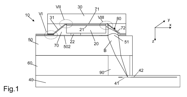
Figure 1 shows a first exemplary embodiment of an optical
assembly 10 according to the present invention. The optical
assembly 10 comprises an optical emitter 20 capable of
generating a beam B of optical radiation. The beam B is
oriented parallel to the space coordinate x in Figure 1 when
it leaves the optical emitter 20. A cap unit 30 carries the
optical emitter 20.
The optical assembly 10 further comprises a photonic chip 40,
an intermediate chip 50 and an interposer chip 60. The
intermediate chip 50 is arranged between the cap unit 30 and
the photonic chip 40. The interposer chip 60 is arranged
between the intermediate chip 50 and the photonic chip 40.
CA 03095662 2020-09-30
WO 2019/201576 PCT/EP2019/058027
12
The cap unit 30 comprises a recess 70 with a bottom section
71 and a sidewall 72. The optical emitter 20 is mounted on
the bottom section 71 of the recess 70. A section of the
sidewall 72 forms a mirror section 80 that is angled with
respect to the bottom section 71 and configured to reflect
the beam B of optical radiation towards a coupler 41 of the
photonic chip 40. The coupler is connected to a waveguide 42
that extends in the space coordinate x in Figure 1 and
therefore in the same direction as the beam B before the beam
B is reflected by the mirror section 80.
The cap unit 30 preferably comprises a (110)-oriented
semiconductor substrate in which the recess 70 is preferably
etched. If the recess 70 is fabricated by anisotropic
etching, the mirror section 80 is formed by a (111)-oriented
surface. In a (110)-oriented semiconductor substrate, the
(111)-oriented mirror section 80 has an angle of 54,75 with
respect to the space coordinate z in Figure 1 and an angle of
35,25 with respect to the space coordinate x in Figure 1.
In order to improve the coupling efficiency between the
mirror section 80 and the coupler 41, the intermediate chip
50 may comprise a lens 51. The lens 51 is formed at a lens
section of the intermediate chip's surface that faces the cap
unit 30. The lens 51 is configured to focus the reflected
optical beam B towards the coupler 41.
The interposer chip 60 has a front surface that faces the
intermediate chip 50 and a backside surface that faces the
photonic chip 40. In the backside surface, a hole 90 has been
fabricated. The hole 90 is situated in the beam path between
the lens 51 and the coupler 41.
CA 03095662 2020-09-30
WO 2019/201576 PCT/EP2019/058027
13
The hole 90 may be a through-hole that extends from the front
surface to the backside surface of the interposer chip 60.
The hole 90 may be empty as shown in Figure 1.
The front side of the cap unit 30 may be bonded on the outer
surface of the intermediate chip 50, i.e. the surface where
the lens 51 is formed. The bonding section is marked by
reference numeral VI in Figure 1 and will be explained in
further detail with reference to Figure 6.
Figure 1 further shows that a first electrical contact 21 of
the optical emitter 20 is connected to a conductive layer 31
of the cap unit 30. The conductive layer 31 extends from the
bottom section 71 of the recess 70 to the bonding section VI.
A portion of the first electrical contact 21 and the
conductive layer 31 is marked by reference numeral VII in
Figure 1 and will be explained in further detail with
reference to Figure 7.
Figure 1 further shows that the conductive layer 31 of the
cap unit 30 may cover the sidewall 72 and form the mirror
section 80. A portion of the conductive layer 31 is marked by
reference numeral VIII in Figure 1 and will be explained in
further detail with reference to Figure 8.
An advantage of the embodiment of Figure 1 is that the
vertical sandwich structure in combination with the
integrated lens provides a high coupling efficiency at low
manufacturing costs.
Figure 2 shows a second exemplary embodiment of an optical
assembly 10 according to the present invention. In this
embodiment, a rotator 110 is arranged within the hole 90 of
CA 03095662 2020-09-30
WO 2019/201576 PCT/EP2019/058027
14
the interposer chip 60. The rotator 110 preferably rotates
the polarization of the optical radiation by 45 and may
reduce the feedback of radiation into the optical emitter 20.
Figure 3 shows a third exemplary embodiment of an optical
assembly 10 according to the present invention. In this
embodiment, a rotator 110 and a X/2 waveplate 111 are
arranged within the hole 90 of the interposer chip 60. The
rotator 110 preferably rotates the polarization of the
optical radiation by 45 . The rotator 110 and the X/2
waveplate 111 may reduce the feedback of radiation into the
optical emitter 20.
Figure 4 shows a fourth exemplary embodiment of an optical
assembly 10 according to the present invention. In this
embodiment, a rotator 110, a polarizer 112 and a X/2
waveplate 111 are arranged within the hole 90 of the
interposer chip 60. The rotator 110 preferably rotates the
polarization of the optical radiation by 45 . The rotator
110, the polarizer 112 and the X/2 waveplate 111 may reduce
the feedback of radiation into the optical emitter 20.
In the embodiments of Figures 2, 3 and 4, the rotator 110 can
either be self-magnetized or externally magnetized. As shown
in Figure 23, the rotator 110 may be located inside a micro-
package 110a and one or more external magnets 110b may be
placed outside of the micro-package 110a. In the latter case
preferably two external magnets 110b are preferably glued
onto the outer sidewalls of the micro-package 110a opposite
to each other.
Figure 5 shows a further exemplary embodiment of an optical
assembly 10 according to the present invention. In this
CA 03095662 2020-09-30
WO 2019/201576 PCT/EP2019/058027
embodiment, the intermediate chip 50 and the interposer chip
60 are bonded together by an intermediate oxide layer 120.
The interposer chip 60, the intermediate chip 50 and the
intermediate oxide layer 120 can therefore be formed by a
5 single pre-processed SOI-chip (sandwich). The hole 90 may be
a blind hole that is etched into the pre-processed SOI-chip.
The hole 90 may extend from the backside surface of the
interposer chip 60 through the interposer chip 60 and through
10 the intermediate oxide layer 120 to the intermediate chip 50.
The hole 90 may be at least partly filled with a rotator 110
as shown in Figure 2, a rotator 110 and a X/2 waveplate 111
as shown in Figure 3, or a rotator 110, a polarizer 112 and a
X/2 waveplate 111 as shown in Figure 4.
Figure 6 shows the bonding section VI of Figure 1 in further
detail. In the embodiment of Figure 6, the intermediate chip
50 comprises a first conductive layer 501, a second
conductive layer 502, an isolation layer 503 and a silicon
substrate 504. The isolation layer 503 is arranged between
the first and second conductive layer 501, 502 and insulates
the first and second conductive layer 501, 502 from one
another. The isolation layer 503 of the intermediate chip 50
may form an antireflection layer on top of the lens 51.
The first conductive layer 501 is bonded with the conductive
layer 31 of the cap unit 30 via solder 150 and therefore
electrically connected with the first electrical contact 21
of the optical emitter 20.
The second conductive layer 502 may be electrically connected
with a second electrical contact 22 of the optical emitter 20
(see Figure 1).
CA 03095662 2020-09-30
WO 2019/201576 PCT/EP2019/058027
16
Figure 7 shows the section VII of Figure 1 in further detail.
The conductive layer 31 is connected to the first electrical
contact 21 of the optical emitter 20.
In order to provide a platform for the optical emitter 20,
the conductive layer 31 of the cap unit 30 may be thicker in
the contact area where the optical emitter 20 is located than
outside this contact area. To this end, the conductive layer
31 of the cap unit 30 may consist of two or more sublayers
31a, 31b in the contact area as shown. Additionally or
alternatively, a conductive pad may located between the
optical emitter 20 and the conductive layer 31.
Figure 8 shows the portion VIII of Figure 1 in further
detail. A solder-stop during the fabrication avoids that
solder 150 fills the gap 160 between the mirror section 80
and the first electrical contact 21 of the optical emitter
20. The conductive layer 31 forms a reflection coating on the
mirror section 80.
An exemplary embodiment of the lens 51 of Figure 1 is
depicted in further detail in Figures 9, 10 and 11.
Figure 9 shows a top view of the lens 51. The lens 51
comprises a first axis Al parallel to the space coordinate x
and a second axis A2 that is perpendicular to the first axis
Al and parallel to the space coordinate y. The direction of
the first axis corresponds to the emission direction of the
optical emitter 20.
In Figures 10 and 11, the height H of the lens 51 is depicted
over the space coordinates x and y, respectively. The radius
CA 03095662 2020-09-30
WO 2019/201576 PCT/EP2019/058027
17
R1 of the curvature of the lens 51 along the first axis Al
differs from the radius R2 of the curvature along the second
axis A2. Preferably, the radius R1 of the curvature along the
first axis Al is between 5% and 15 % larger than the radius
R2 along the second axis A2.
The following parameters are considered advantageous:
250 pm R2 310 pm
250 pm R1 330 pm
1.02 Al/A2 1.15
Figure 12 shows a further exemplary embodiment of an optical
assembly 10 according to the present invention. In this
embodiment, a heat spreader 180 is mounted on a backside of
the cap unit 30. The backside is located opposite to the
front side where the recess 70 is formed.
Figure 13 shows an exemplary embodiment of a process flow
that allows fabricating parts of the optical assembly 10. The
method according to Figure 13 refers to a wafer scale process
where an intermediate wafer (also referred to as lens wafer)
and an interposer wafer are bonded before etching holes 90.
The method according to Figure 13 comprises the steps of:
¨ bonding an intermediate wafer (for the future intermediate
chips 50) and an interposer wafer (for the future
interposer chips 60) by an intermediate oxide layer 120
(step 1001),
¨ etching holes 90 into the intermediate wafer (step 1002),
¨ providing an antireflection coating on the backside of the
intermediate wafer (step 1003),
¨ etching lenses 51 on the outside surface of the
intermediate wafer (step 1004),
CA 03095662 2020-09-30
WO 2019/201576 PCT/EP2019/058027
18
¨ depositing the second conductive layer 502 (for the n-
contacts of the optical emitters 20) on the outside
surface of the intermediate wafer (step 1005),
¨ depositing the isolation layer 503 on top of the second
conductive layer 502 (step 1006),
¨ depositing the first conductive layer 501 (for the p-
contacts of the optical emitters 20) on top of the
isolation layer 503 (step 1007),
¨ depositing solder 150 on top of the first conductive layer
501 (step 1008),
¨ masking a cap wafer (step 2001),
¨ etching recesses 70 into the cap wafer (step 2002),
¨ depositing a conductive layer 31 (step 2003),
¨ providing platforms for the optical emitters 20 (step
2004),
¨ depositing solder-stops adjacent to mirror sections 80
(step 2005),
¨ depositing solder 150 (step 2006),
¨ mounting optical emitters 20 (e.g. a lasers) in the
recesses 70 and forming cap units 30 that carry the
optical emitters 20 (step 2007),
¨ mounting the cap wafer on the intermediate wafer (step
2008),
¨ separating the resulting composite for micro-packages
(step 2009),
¨ optionally mounting rotators 110 (step 2010).
Figure 14 shows another exemplary embodiment of a process
flow that allows fabricating parts of the optical assembly
10. The method according to Figure 14 refers to a chip scale
process where an intermediate wafer (also referred to as lens
wafer) and an interposer wafer are bonded before etching
CA 03095662 2020-09-30
WO 2019/201576
PCT/EP2019/058027
19
holes 90. The method according to Figure 14 comprises the
steps of:
¨ bonding an intermediate wafer (for the future intermediate
chips 50) and an interposer wafer (for the future
interposer chips 60) by an intermediate oxide layer 120
(step 1001),
¨ etching holes 90 into the intermediate wafer (step 1002),
¨ providing an antireflection coating on the backside of the
intermediate wafer (step 1003),
¨ etching lenses 51 on the outside surface of the
intermediate wafer (step 1004),
¨ depositing the second conductive layer 502 (for the n-
contacts of the optical emitters 20) on the outside
surface of the intermediate wafer (step 1005),
¨ depositing the isolation layer 503 on top of the second
conductive layer 502 (step 1006),
¨ depositing the first conductive layer 501 (for the p-
contacts of the optical emitters 20) on top of the
isolation layer 503 (step 1007),
¨ depositing solder 150 on top of the first conductive layer
501 (step 1008),
¨ separating the intermediate wafer to form separate base
units (step 1009),
¨ masking a cap wafer (step 2001),
¨ etching recesses 70 into the cap wafer (step 2002),
¨ depositing a conductive layer 31 (step 2003),
¨ providing platforms for the optical emitters 20 (step
2004),
¨ depositing solder-stops adjacent to mirror sections 80
(step 2005),
¨ depositing solder 150 (step 2006),
CA 03095662 2020-09-30
WO 2019/201576 PCT/EP2019/058027
¨ mounting optical emitters 20 (e.g. a lasers) in the
recesses 70 and forming cap units 30 that carry the
optical emitters 20 (step 2007),
¨ separating the resulting cap wafer in order to form
5 separate cap units 30 (step 3000),
¨ mounting the cap units 30 of step 3000 on the base units
of step 1009 (step 3001),
¨ optionally mounting rotators 110 (step 2010).
10 Figure 15 shows another exemplary embodiment of a wafer scale
process to fabricate parts of the optical assembly 10. The
method according to Figure 15 largely corresponds to the
wafer scale process of Figure 13. In contrast to Figure 13,
step 1002 is carried out before 1001. In other words, the
15 intermediate wafer and the interposer wafer are bonded after
etching the holes 90.
Figure 16 shows another exemplary embodiment of a chip scale
process to fabricate parts of the optical assembly 10. The
20 method according to Figure 16 largely corresponds to the chip
scale process of Figure 14. In contrast to Figure 14, step
1002 is carried out before 1001. In other words, the
intermediate wafer and the interposer wafer are bonded after
etching the holes 90.
The wafer-scale fabrication as described above with reference
to Figures 13 and 15 allows a cost-efficient mass production
of optical assemblies according to the present invention.
Figure 17 shows an exemplary embodiment of a silicon cap
wafer 200 consisting of (110)-Material. The recess 70 is
etched anisotropically without etch-stop layer. The mirror
section 80 is formed by a (111)-plane.
CA 03095662 2020-09-30
WO 2019/201576 PCT/EP2019/058027
21
Figure 18 shows an exemplary embodiment of a silicon cap
wafer 200 consisting of SOI-material having a silicon top
layer 201, an oxide layer 202, and a bottom layer 203. At
least the silicon top layer 201 consists of (110)-Material.
The recess 70 is etched anisotropically. The oxide layer 202
serves as an etch-stop layer. Again, the mirror section 80 is
formed by a (111)-plane.
Figures 19 and 20 show a recess 70 after applying a solder-
stop 161. In Figure 19, the solder-stop 161 is arranged
between the bottom of the recess 70 and the mirror section
80. In Figure 20, the solder-stop 161 surrounds the mirror
section 80.
Figure 21 shows an exemplary embodiment of a marker 210 that
is etched in the (110)-surface of the silicon cap wafer 200.
The marker 210 is delimited by (111)-oriented surfaces. The
marker 210 facilitates the mounting of the cap unit 30 with
respect to the interposer chip 60. The marker 210 is
preferably located adjacent to the recess 70.
Figure 22 shows a further exemplary embodiment of an optical
assembly 10 according to the present invention. In this
embodiment, the entire lens 51 is embedded in a recess 51a in
the outer surface of the intermediate chip 50. The lens 51 is
formed by the bottom of the recess 51a and located below the
plane of the second conductive layer 502.
An advantage of the exemplary embodiments of optical
assemblies as described above with reference to Figures 1-22
is that the vertical sandwich structure thermally separates
the optical emitter 20 from the photonic chip 40. Therefore,
CA 03095662 2020-09-30
WO 2019/201576 PCT/EP2019/058027
22
the thermal impact of the optical emitter 20 on the photonic
chip 40 is very small. The thermal impact may be further
reduced by means of the heat spreader 180 as explained with
reference to Figure 12.
Figure 24 shows an exemplary embodiment of a partly chip
scale and partly wafer scale process to fabricate parts of
the optical assembly 10. The method according to Figure 24
largely corresponds to the wafer scale process of Figure 13.
In contrast to Figure 13, the step 1009a of separating the
lenses is introduced before carrying out step 2008a of
mounting the lenses on the cap wafer. In other words, the
lenses are separated and soldered onto the cap wafer, before
the laser micropackages are separated.
Figure 25 shows an exemplary embodiment of a partly chip
scale and partly wafer scale process to fabricate parts of
the optical assembly 10. The method according to Figure 25
largely corresponds to the wafer scale process of Figure 13.
In contrast to Figure 13, a step 3000a of cap separation is
introduced before carrying out step 2008b of mounting the
caps on the lens wafer. In other words, the caps are
separated and soldered onto the lens wafer, before the laser
micropackages are separated.
The various embodiments and aspects of embodiments of the
invention disclosed herein are to be understood not only in
the order and context specifically described in this
specification, but to include any order and any combination
thereof. Whenever the context requires, all words used in the
singular number shall be deemed to include the plural and
vice versa. Whenever the context requires, all options that
CA 03095662 2020-09-30
WO 2019/201576 PCT/EP2019/058027
23
are listed with the word "and" shall be deemed to include the
world "or" and vice versa, and any combination thereof.
In the drawings and specification, there have been disclosed
a plurality of embodiments of the present invention. The
applicant would like to emphasize that each feature of each
embodiment may be combined with or added to any other of the
embodiments in order to modify the respective embodiment and
create additional embodiments. These additional embodiments
form a part of the present disclosure and, therefore, the
applicant may file further patent claims regarding these
additional embodiments at a later stage of the prosecution.
Further, the applicant would like to emphasize that each
feature of each of the following dependent claims may be
combined with any of the present independent claims as well
as with any other (one ore more) of the present dependent
claims (regardless of the present claim structure).
Therefore, the applicant may direct further patent claims
towards other claim combinations at a later stage of the
prosecution.
CA 03095662 2020-09-30
WO 2019/201576
PCT/EP2019/058027
24
Reference Signs
optical assembly
optical emitter
5 21 first electrical contact
22 second electrical contact
cap unit
31 conductive layer
31a sublayer
10 31b sublayer
photonic chip
41 coupler
42 waveguide
intermediate chip
15 51 lens
51a recess
interposer chip
recess
71 bottom section
20 72 sidewall
mirror section
hole
110 rotator
110a micro-package
25 110b external magnet
111 X/2 waveplate
112 polarizer
120 intermediate oxide layer
150 solder
30 160 gap
161 solder-stop
180 heat spreader
200 silicon cap wafer
CA 03095662 2020-09-30
WO 2019/201576
PCT/EP2019/058027
201 silicon top layer
202 oxide layer
203 bottom layer
210 marker
5 501 first conductive layer
502 second conductive layer
503 isolation layer
504 substrate
Al first axis
10 A2 second axis
R1 radius
R2 radius
B beam of optical radiation
x space coordinate
15 y space coordinate
z space coordinate