Note: Descriptions are shown in the official language in which they were submitted.
1
RECONFIGURABLE QUANTUM ROUTING
RELATED APPLICATIONS
[0001] This application claims priority from U.S. Patent Application
Serial
No. 16/012543, filed 19 June 2018.
[0002] U.S. Patent Application Serial No. 16/012543 issued 21 January
2020 as U.S.
Patent No. 10,540,603.
TECHNICAL FIELD
[0003] The present invention relates generally to quantum and classical
digital
superconducting circuits, and specifically to reconfigurable quantum routing.
BACKGROUND
[0004] A fundamental challenge for quantum computation and simulation is
to construct
a large-scale system of highly connected coherent qubits to perform various
operations.
Superconducting qubits utilize macroscopic circuits to process quantum
information and are a
promising candidate towards this end. Recently, materials research and circuit
optimization has
led to significant progress in qubit coherence. Superconducting qubits can now
perform
hundreds of operations within their coherence times, allowing for research
into complex
algorithms such as error correction. In many applications, it is desirable to
combine these high-
coherence qubits with tunable inter-qubit coupling, since it would allow for
both coherent local
operations and dynamically varying qubit interactions. For quantum
computation, this would
provide isolation for single-qubit gates while at the same time enabling fast
two-qubit gates that
minimize errors from decoherence.
Date Recue/Date Received 2022-01-13
CA 03096490 2020-10-06
WO 2019/245740 PCT/1JS2019/035607
2
SUMMARY
[0005] One example includes a reconfigurable quantum router system. The
system
includes first, second, and third quantum objects respectively connected to
first, second, and
third ports of a quantum router. The quantum router includes two variable-
inductance coupling
elements each in an RF-SQUID, at least two of the variable-inductance coupling
elements being
connected to at least one shared inductor such that their respective RF-SQUIDs
share the
inductor in common. The quantum router further includes first and second
control flux lines,
wherein one of the flux control lines is configured to inductively provide a
static current to at
least two of the variable-inductance coupling elements and the other of the
control flux lines is
configured to provide a dynamic current to at least two of the variable-
inductance coupling
elements. The quantum router further includes first, second, and third
resonators by which the
first, second. and third quantum objects are respectively each connected to at
least one of the RE-
SQUIDs, such that each quantum object can be placed arbitrarily distantly from
the RF-SQUIDs
on a chip. Actuation of the direction of the dynamic current couples at least
the first quantum
object to only one of the first or second quantum objects based on the dynamic
current direction
to provide reconfigurable quantum routing.
[0006] Another example includes a method of reconfigurable quantum routing.
A static
control signal is provided to one of a first flux line that is inductively
coupled to two
RF-SQUIDs via at least one common inductor to induce a current split between
variable
inductance coupling elements in respective ones of the RF-SQUIDs, or a second
flux line that is
inductively coupled to at least two RF-SQUIDs via other inductors in each of
them. A dynamic
control signal is provided to the other of the first flux line or the second
flux line, such that the
difference between induced common flux current and induced dynamic flux
current places at
least one of the variable inductance coupling elements in one of a high or low
inductance state
and places at least another of the variable inductance coupling elements in
the other of the high
or low inductance state. The direction of the dynamic control signal is
actuated to couple at least
a first quantum object (e.g., a qubit) to only one of at least two other
quantum objects, based on
the dynamic control signal direction.
CA 03096490 2020-10-06
WO 2019/245740 PCT/1JS2019/035607
3
[0007] Yet another example includes a reconfigurable quantum router. The
quantum
router includes first, second, and third ports each coupleable to a respective
qubit, and first,
second, and third resonators each respectively connected between the first,
second, and third
ports and an RF-SQUID bridge. The RF-SQUID bridge includes a first Josephson
junction
connected between the first resonator and the second resonator, and a second
Josephson junction
connected between the first resonator and the third resonator. First and
second flux lines are
arranged to switch the inductance of the Josephson junctions between high and
low inductance
states to selectively couple or uncouple qubits connected to the ports.
BRIEF DESCRIPTION OF THE DRAWINGS
[0008] FIG. lA is a block diagram of an example reconfigurable quantum
router system.
[0009] FIG. 1B is a diagram showing both of two alternate muting states of
a first
example reconfigurable quantum router.
[0010] FIG. IC is a diagram showing a first of two alternate routing states
of a second
example reconfigurable quantum router (a "bar" state).
[0011] FIG. 1D is a diagram showing a second of two alternate routing
states of the
second example reconfigurable quantum router (a "cross" state).
[0012] FIG. 2 is a circuit diagram of an example reconfigurable quantum
router.
[0013] FIG. 3 is a diagram showing hybridized resonators producing
frequency-split
even and odd modes.
[0014] FIG. 4 is a logical-level quantum circuit illustration for a parity
check operation
between two logical qubits.
[0015] FIG. 5 is a quantum circuit segment illustration for the operation
of FIG. 4.
[0016) FIG. 6 is a circuit diagram of an example reconfigurable quantum
router.
[0017] FIG. 7 is an annotated logical-level quantum circuit illustration
for Toff li
distillation.
[0018] FIGS. 8A, 8B, and 8C are flow charts illustrating example methods of
reconfigurable quantum routing.
4
DETAILED DESCRIPTION
[0019] Performing quantum algorithms on a physical quantum processor can
present a
challenge when different circuit blocks, which can be remotely located on the
chip, need to
interact sequentially with another circuit block. This situation may arise,
for example, in
performing parity check operations on a logical level, or in state
distillation routines on both
physical and logical levels. One challenge of routing of quantum information
is that "signal
path" (i.e., the connectivity) of quantum objects must be reconfigurable in
real time.
[0020] A 2-port, tunable bus-mediated coupling that uses a radio frequency
superconducting quantum interference device (RF-SQUID) as a tunable coupling
element
embedded in the center point of a half-wave bus resonator is described in U.S.
patent application
publication No. 2017/0212860 Al. The effective coupling between a qubit
connected to the Port
1 of the bus and a qubit connected to Port 2 of the bus is observable as a
balance between two
contributions (even and odd modes of the bus) having opposite signs and
variable strengths.
This coupling does not permit routing of quantum information between quantum
objects, or for
more than two quantum objects to be connected together to exchange
information. Thus, even
with such a coupling, connectivity between qubits is fixed in the design of
the chip: although the
strength of the coupling can be field-tunable, the topology of the circuit
cannot be changed. As
described herein, the sought-after real-time reconfigurability of quantum
object connectivity can
be provided with either or both of a single-pole double-throw switch and a
cross-point switch.
[0021] Thus, this disclosure relates generally to reconfigurable quantum
routing in
superconducting circuits, for example, to provide reconfigurable connectivity
between qubits or
other quantum objects. This disclosure particularly provides both a single-
pole double-throw
switch and a cross-point switch for the connectivity configuration of a
quantum circuit. In
various examples, one or more variable inductance coupling elements are placed
between qubits
or other quantum objects that may reside in separate remote superconducting
systems. The
variable inductance coupling elements can each be adjusted between a strongly
coupled state and
a decoupled (or isolation) state between quantum objects in addition to
various states of
Date Recue/Date Received 2022-01-13
CA 03096490 2020-10-06
WO 2019/245740 PCT/US2019/035607
intermediate coupling strengths in between. In this manner, manipulation can
be performed on
state information of isolated qubits in a decoupled state, while this state
information can be
exchanged between qubits during a strongly coupled state, for example.
Furthermore, state
information can be manipulated and passed between qubits without destroying
the state
inlbrrnation of the originating qubit in an intermediate coupling strength
state between qubits. In
some examples, the variable inductance coupling elements can be Josephson
junctions. Each
variable inductance coupling element can be arranged as a single Josephson
junction or a series
array of N Josephson junctions, each having a critical current N times larger
than the original
(single) Josephson junction.
[0022] Some example reconfigurable quantum routers can include one or more
Josephson junctions embedded at a dovetail node of a split half-wave resonator
bus. The
RRSQUID facilitates bus-mediated dispersive interaction between connected
qubits or other
quantum objects for coupling. The advantage of bus-mediated coupling, as
opposed to direct
inductive coupling, is that the quantum objects can be physically placed
remotely from each
other, for example, in separate circuit blocks on the quantum processor chip.
The advantage of a
reconfigurable quantum router is that it permits signals to be routed between
quantum objects as
desired and at the coupling or interaction strengths desired. Thus, for
example, interaction
strengths can be calibrated and trimmed in the field to compensate for
variability in
manufacturing processes, and can be controlled in real time as part of a
computation protocol.
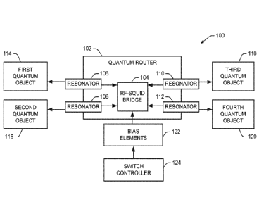
[0023] FIG. 1A illustrates an example superconducting system 100 with
reconfigurable
quantum routing. The superconducting system 100 includes three or four quantum
objects (e.g.,
qubits) 114, 116, 118, 120. As illustrated, one pair of quantum objects is
connected on each side
of router 102, but one side of router 102 may be connected to only one quantum
object. Each
quantum object can, for example, be part of a qubit system that belongs to a
logical block that
can perform different logical operations such as different gate operations,
error correction
operations, memory operations, or any of a variety of other superconducting
operations.
Connections between the quantum objects 114, 116, 118, 120 can be bus-
mediated, allowing the
quantum objects 114, 116, 118, 120 to reside at arbitrarily distant parts of a
chip on which they
6
are fabricated, for example. Router 102 thus couples or uncouples the quantum
objects via a
reconfigurable RF-SQUID bridge 104 (consisting, for example, of two or four RF-
SQUIDs) and
further via resonators (e.g., transmission lines) 106, 108, 110, 112. Router
can thereby couple
one quantum object (e.g., 114) to one of two other quantum objects (e.g.,
either of 118 or 120),
as shown in FIG. 1B, or can couple two quantum objects (e.g., 114, 116) to two
other quantum
objects (e.g., 118, 120) in bar or cross fashions, as shown in FIGS. 1C and
1D, respectively. (In
FIG. 1B, the two broken lines in router 102 indicate alternate couplings,
whereas those in
FIG. 1C indicate simultaneous couplings, as do those in FIG. 1D.)
[0024] Quantum router 102 can thus, for example, constitute a compound
bus composed
of three resonators (e.g., 106, 110, 112) and a two-Josephson-junction coupler
104, or of four
resonators (106, 108, 110, 112) and a four-Josephson-junction coupler 104, in
either case having
bias elements 122 (e.g., a static flux bias and a control flux) to activate
the switching
functionality of the router 102. The system 100 can be implemented in any of a
variety of
superconducting circuit systems to provide coupling and decoupling between
quantum objects.
The signals between the coupled objects can be, for example, microwave signals
that are
implemented in a control scheme for a quantum circuit, such as performing a
gate or a readout
operation on a qubit, or to perform one of a variety of algorithms, such as
those discussed herein.
As another example, the signals can be a signal pulse, a communication signal,
or a control
command signal. The system 100 can operate at cryogenic temperatures, can
dissipate
substantially no power, and can be controlled with single flux quantum (SFQ)
compatible
signals.
[0025] System 100 can include a switch controller 124 and bias elements
122. The
RF-SQUID bridge 104 can employ variable inductance coupling elements
controlled by
magnetic flux via the bias elements 122 and the switch controller 124 to
couple and decouple
connected quantum objects based on a selected mode (i.e., between either of
the modes depicted
in FIG. 1B, or between the modes separately depicted in FIGS. 1C and 1D,
depending on the
configuration of the router 102). The variable inductance coupling elements
can each include,
for example, one or more Josephson junctions. The one or more Josephson
junctions can have a
Date Recue/Date Received 2022-01-13
CA 03096490 2020-10-06
WO 2019/245740 PCT/1JS2019/035607
7
first inductance when no current or a low current is induced in the respective
RF-SQUID, and a
second inductance when a current or a higher current is induced in the
respective RF-SQUID that
is at a predetermined threshold that generates or induces a flux, for example,
greater than
about 0.1 (Do and less than about 0.45 00, where (1)0 is equal to a flux
quantum. The first such
inductance (e.g., fi/2eIc., where It is Planck's constant divided by 22t, e is
electron charge and Ic
is the critical current of the Josephson junction) can provide coupling
between quantum objects,
while the second such inductance (e.g., a large inductance value) can provide
decoupling
between the quantum objects.
[0026] FIG. 2 illustrates an example reconfigurable quantum router 200
arranged as a
single-pole double-throw (SPDT) reconfigurable bus coupler, which can
function, for example,
as a one-to-two multiplexer. Resonators TLI, TL2, and TL3 are coupleable via
respective
capacitors CI. C2 and C3 to quantum objects (e.g., qubits) that can be
connected at Ports 1-3
respectively. Each resonator can support coupling to a plurality of qubits,
either capacitively, as
illustrated in FIG. 2, or inductively, or combination of both, as described in
U.S. patent
No. 9,501,748, which is herein incorporated by reference. Each of the
resonators TL1, TL2, and
TL3 can be, for example, a quarter-wave shorted transmission line resonator,
configured such
that resonator TLI and TL-, are both connected via RF-SQUID couplers to
resonator TL3. In the
illustrated example, a first RF-SQUID is composed of Josephson junction J1
connected to
inductors Li and L3 to form a first superconducting loop, and a second RF-
SQU1D is composed
of Josephson junction J2 connected to inductors L2 and L3 to form a second
superconducting
loop, where both loops share a common inductor L3. The Josephson inductance of
each of the
Josephson junctions Ji and J2 is greater than the total linear inductance of
the respective loops
(i.e., Lji > Li + L3 and LI2 > L2 -I- L3).
[0027] In circuit 200, Josephson junctions J1 and J2 function as variable
inductance
elements, as determined by the magnetic flux enclosed in each respective RF-
SQUID loop.
When an RF-SQUID encloses a flux clkm that is substantially zero, the
inductance of the junction
in the RF-SQUID has a value equal to ftl2e1c, where It is Planck's constant
divided by 2x, e is the
electron charge, and lc is the junction critical current. When the RF-SQUID
encloses a flux
CA 03096490 2020-10-06
WO 2019/245740
PCT/1JS2019/035607
8
(1:00FF that is a significant fraction of 00/2, e.g., greater than about 0.1
(100 and less than about
0.45 (Do, the inductance of the junction diverges. Therefore, when the RF-
SQUID formed by Ji,
Li, and L3, encloses a flux (Dorf, the coupling between resonators TL1 and TL3
is essentially
zero, and the qubits connected to the respective resonators do not interact
(e.g., they do not
exchange information). However when the same RF-SQUID encloses a flux ON, the
resonators
TLI and TL3 become coupled with a coupling strength gc, and hybridize to
support two
oscillation modes as shown in diagram 300 FIG. 3. The qubits that are
connected to the
respective resonators experience a non-zero effective coupling, geff in FIG.
3. Similarly, the
coupling between resonators TL, and TL3 can be turned on or off based on a
flux (1:00N or Om
enclosed by the RF-SQUID formed by junction J2 and inductors L2 and L3, and
similarly the
effective coupling between the qubits that connect to the respective
rcsonators can be turned on
or off.
[0028] The
fluxes applied to the two RF-SQUIDs can be controlled via two flux-bias
lines, indicated in FIG. 2 by differential flux line 202 (between nodes DF+
and DF-) and
common flux line 204 (between nodes CF+ and CF-). A current flowing in the
differential flux
control line 202 induces a current in inductors Li and L2 through respective
mutual inductances
Mi and M2. A current flowing in the common flux control line 204 induces a
current in inductor
L3 through mutual inductance M3. The current induced in inductor L3 splits to
flow through
inductors Li and L2 such that in one of the inductors the current adds to that
induced by the
differential flux control line, and in the other it subtracts. In other words,
the two control
currents can combine to produce any flux configuration in the two RF-SQUIDs.
In particular,
the common flux can be static and set at (41:00FF + (DoN) /2 and the
differential flux can be toggled
between (4001,r, - (DoN) /2 and -(1)ow - (DoN) /2, so that in a first
configuration the first RF-SQUID
encloses a total flux (1)0N and the second RF-SQUID encloses a flux (1:00EF,
whereas in a second
configuration the first RF-S QUID encloses a flux cloorr, while the second RF-
SQUID encloses a
flux ON. Therefore, in the first configuration qubits connected to TL3 have an
effective
coupling to qubits connected to TLI (but not to qubits connected to TL2),
whereas in the second
configuration the qubits connected to TL3 have an effective coupling to those
connected to Th.)
CA 03096490 2020-10-06
WO 2019/245740 PCT/1JS2019/035607
9
(but not to qubits connected to TIA). The functionalities of common flux line
204 and
differential flux line 202 can be interchanged, with differential line 202
being held static and
common line 204 being toggled, to result in a circuit that functions
similarly. In either case,
because no net power is delivered between the ports, the functioning of
circuit 200 differs from
the actuation of a SPDT microwave switch to control delivery of microwave
power in that
circuit 200 can control an effective dispersive bus-mediated coupling between
quantum objects
without power delivery between ports.
[0029] Thus in an example functioning of circuit 200, two RF-SQUIDs
commonly
coupled by inductor L3 can be provided common flux via line 204 that yields an
induced current
coming out of inductor L3 that in turn is shared in opposite directions
between Josephson
junctions J1 and J2. Such current is therefore either contributorily added or
subtracted from the
current induced by differential flux line 202, which flows in the same
direction through each of
inductors Li and L2. Thus, one of Josephson junctions J1, J2 is in a high
inductance state while
the other is in a low inductance state, the inductance states of the
respective Josephson junctions
being based entirely on the direction of the current flowing through
differential flux line 202 in
this example. Common flux current through line 204 stays steady, while
differential flux current
through line 202 is actuated in each of two directions, depending on the
intended configuration
of switch 202 to change the coupling between one of the qubits (for example)
on one of Port 1 or
Port 2 with the qubit (for example) on Port 3. However, as already noted, the
roles of lines 202
and 204 are interchangeable.
[0030] FIGS. 4 and 5 together show an example of a logical-level quantum
circuit that
can use circuit 200 to provide reconfigurable quantum routing. Quantum circuit
segment 500 in
FIG. 5 performs a parity check operation between two logical qubits 502, 504,
using a logical
ancilla 506. Each of the logical qubits 502, 504 may be composed of an error-
corrected
collection of physical qubits, and as such may be located at a separate
physical circuit block on a
quantum processor chip. Circuit 200, with its dual RE-SQUID construction
represented by
circuit portion 508 in FIG. 5. allows for a remote connection (i.e., over a mm-
scale distances)
between the circuit blocks. The circuit 400 of FIG. 4 illustrates the sequence
of connections.
CA 03096490 2020-10-06
WO 2019/245740 PCT/1JS2019/035607
The first logical CNOT gate 402 corresponds to the control fluxes being
configured such that the
ancilla 506, whose physical qubits are connected to TL3, is coupled via the RF-
SQUIDs 508 to
the second logical data qubit 504, whose physical qubits are connected to TL2.
After the
function of the first CNOT gate 402 is performed, the control fluxes can be
switched so that the
first logical data qubit 502, whose physical qubits are connected to TLI, is
coupled to the
ancilla 506 and the function of the second logical CNOT gate 404 can thereby
be performed.
[0031] FIG. 6 illustrates another example reconfigurable quantum router 600
arranged as
a cross-point reconfigurable bus coupler. Similar to reconfigurable quantum
router 200 of
FIG. 2, circuit 600 also uses RF-SQUIDs to couple resonators, in this case
resonators TL1, TL2,
TL3, TL, which can be, for example, short-terminated quarter-wave resonators.
In the illustrated
example, a first RF-SQUID is composed of Josephson junction Ji connected to
inductors Li and
L3 to form a first superconducting loop, a second RF-SQUID is composed of
Josephson junction
J2 connected to inductors L2 and L4 to form a second superconducting loop, a
third RF-SQU1D is
composed of Josephson junction J3 connected to inductors Li and 14 to form a
third
superconducting loop, and a fourth RF-SQUID is composed of Josephson junction
J4 connected
to inductors L, and L3 to form a fourth superconducting loop, where the first
and third loops
share a common inductor Li, the second and fourth loops share a common
inductor L2, the first
and fourth loops share a common inductor L3, the second and third loops share
a common
inductor L4. Circuit 600 is also controlled by two flux lines, fluxl 602 and 1
ux2 604, one of
which can be configured as a static DC flux offset while the other is
configured to be controlled
in real time. Thus, for example, fluxl 602 can serve as a common flux line
while flux2 604
serves as a differential flux line, or vice versa.
[0032] Under the condition that equal magnitude currents flow in flux
control
lines 602, 604 in the same direction, the currents induced through Josephson
junctions Ji and J2
cancel, while the currents through Josephson junctions J3 and J4 sum. The
total currents induced
through Josephson junctions J3 and J4 put these Josephson junctions in a high
inductance state,
causing the effective coupling between resonators TL4 and TLI, as well as
between resonators
TL3 and TL2, to vanish. Under such condition, since the currents in Josephson
junctions Ji and J4
CA 03096490 2020-10-06
WO 2019/245740 PCT/1JS2019/035607
11
cancel, these Josephson junctions exhibit a low inductance state and there
exists an appreciable
effective coupling between resonators TL3 and TL1, as well as between
resonators TL4 and TL,.
This condition, wherein Ports I and 3 are coupled. Ports 2 and 4 are coupled,
Ports I and 4 are
uncoupled, and Ports 2 and 3 are uncoupled, may be referred to as a bar state.
[00331 Under the condition that equal magnitude currents flow in flux
control
lines 602, 604 in opposite directions, the induced currents will, by contrast,
add on Josephson
junctions Ji and J2 and cancel on Josephson junctions J3 and J4. In this
configuration there exists
an effective coupling between resonators TL3 and TL2 as well as between
resonators TL4 and
TLI. while the coupling between resonators TL3 and TLI, as well as between
resonators TL4 and
TL2, vanishes. This condition, wherein Ports 1 and 4 are coupled, Ports 2 and
3 are coupled,
Ports 1 and 3 are uncoupled, and Ports 2 and 4 are uncoupled, may be referred
to as a cross state.
[0034] Reconfigurable quantum router 600 in FIG. 6 therefore functions as
a cross point
rcconfigurable bus that can selectively connect pairs of qubits (or groups of
qubits) in response
to two control currents having the same or opposite sign. Thus in an example
of the functioning
of circuit 600, when flux is provided in the same direction through lines 602,
604, pairs of RF-
SQUIDs exhibit respective high or low inductance states to place the switch
600 in a bar
configuration (as shown in FIG. IC), while changing the polarity of one of the
flux lines relative
to the other alters the respective inductance states to place the switch 600
in a cross configuration
(as shown in FIG. 1D). Thus, the Josephson junctions in the RF-SQUIDs of
router 600 are
switched in pairwise fashion.
100351 FIG. 7 illustrates an example quantum algorithm for which cross-
point
reconfigurable bus 600 may be applied. H-to-Toffoli distillation circuit 700
is shown in terms of
the I H)-state implementation of Margolus-Toffoli gates. The algorithm uses
pairwise CNOT
gates 708/710, 712/714, 716/718 with alternating operands, where the circuit
600 facilitates the
swapping of the operands as shown in FIG. 7. CNOT gates 708, 710 are achieved
by bar
state 702; CNOT gates 712, 714 are achieved by cross state 704; and CNOT gates
716, 718 are
achieved by bar state 706. The last CNOT gate 720 in the algorithm can be
achieved using a
fixed coupling between member qubits. Performing the algorithm using circuit
600 alleviates
CA 03096490 2020-10-06
WO 2019/245740 PCT/1JS2019/035607
12
complications that arise due to frequency crowding of the qubits and errors
that may occur when
qubit frequencies are swept across each other. Any algorithm that requires
similar operand
swapping can similarly benefit from the use of circuit 600.
[00361 Multiple of the switches 100, 200, 600 can be concatenated to create
higher-
connectivity configurations. For example, two "Port 3"s of second and third
instances of
router 200 could be connected, respectively, to Port 1 and Port two of a first
instance of
router 200 to result in a one-to-four multiplexer. As another example,
multiple switches 600
could be connected to each other, or one or more routers 200 could be
connected to one or more
routers 600, extending the number of "input" and "output" ports and creating a
greater variety of
switching solutions. In such concatenated examples a single switch controller
124 could be
configured to control the multiple bias elements 122 for multiple or all
concatenated routers.
[0037] FIG. 8A shows an example method 800 of recontigurable quantum
routing. A
static control signal is provided 802 to one of a common flux line that is
inductively coupled to
two RF-SQUIDs via a common inductor to induce a current split between first
and second
variable inductance coupling elements in the respective RF-SQUIDs, or a
differential flux line
that is inductively coupled to the two RF-SQUIDs via other inductors in each
of the RF-SQUIDs
to induce a current flowing unsplit through the first and second variable
inductance coupling
elements. A dynamic control signal is provided 804 to the other of the common
flux line or the
differential flux line, such that the difference between induced common flux
current and induced
dynamic flux current places 806 the first variable inductance coupling element
(e.g., a first
Josephson junction in the first RF-SQUID) in one of a high or low inductance
state and
places 806 the second variable inductance coupling element (e.g., a second
Josephson junction in
the second RF-SQUID) in the other of the high or low inductance state. The
differential and
common flux lines can be configured, for example, like lines 202 and 204 of
circuit 200 shown
in FIG. 2. The direction of the dynamic control signal (provided to one of the
common flux line
or the differential flux line) is actuated 808 to couple a first quantum
object (e.g., a qubit) to
either a second quantum object or a third quantum object, based on the dynamic
control signal
direction. Reconfigurable quantum routing is thereby achieved between the
quantum objects.
CA 03096490 2020-10-06
WO 2019/245740 PCT/1JS2019/035607
13
[0038] FIG. 8B shows another example method 850 of reconfigurable quantum
routing.
A static control signal is provided 852 to one of a first flux line that is
inductively coupled to first
and second RF-SQUIDs via a common first inductor and third and fourth RF-
SQUIDS via a
common second inductor to induce currents split between first and second
variable inductance
coupling elements in the respective first and second RF-SQUIDs and between
third and fourth
variable inductance coupling elements in the respective third and fourth RF-
SQUIDs, or a second
flux line that is inductively coupled to the first and fourth RF SQUIDs via a
common third
inductor and the second and third RF-SQUIDs via a common fourth inductor to
induce currents
split between the first and fourth variable inductance coupling elements and
between the second
and third variable inductance coupling elements. A dynamic control signal is
provided 854 to
the other of the first flux line or the second flux line, such that the
difference between induced
first flux current and induced second flux current in each of the RF-SQUIDs
places 856 two of
the variable inductance coupling elements in one of a high or low inductance
state and
places 856 the other two variable inductance coupling elements in the other of
the high or low
inductance state. The first and second flux lines can be configured, for
example, like lines 602
and 604 of circuit 600 shown in FIG. 6. The direction of the dynamic control
signal is
actuated 858 to couple a first quantum object (e.g., a qubit) to one of a
second quantum object or
a third quantum object and to couple a fourth quantum object to the other of
the second quantum
object or the third quantum object, based on the dynamic control signal
direction.
Reconfigurable quantum routing (in either "bar" or "cross" states) is thereby
achieved between
the quantum objects.
10039] FIG. 8C shows an example method 870 of reconfigurable quantum
routing. A
static control signal is provided 872 to one of a first flux line that is
inductively coupled to at
least two RF-SQUIDs via at least one common inductor to induce at least one
current split
between variable inductance coupling elements in respective ones of the RF-
SQUIDs, or a
second flux line that is inductively coupled to the or another at least two RF-
SQUIDs via other
inductors in each of the RF-SQUIDs. A dynamic control signal is provided 874
to the other of
the first flux line or the second flux line, such that the difference between
induced common flux
CA 03096490 2020-10-06
WO 2019/245740 PCT/1JS2019/035607
14
current and induced dynamic flux current places 876 at least one of the
variable inductance
coupling elements in one of a high or low inductance state and places 876 at
least another of the
variable inductance coupling elements in the other of the high or low
inductance state. The first
and second flux lines can be configured, for example, like lines 204 and 202
of circuit 200
shown in FIG. 2 or like lines 602 and 604 of circuit 600 shown in FIG. 6. The
direction of the
dynamic control signal is actuated 878 to couple at least a first quantum
object (e.g., a qubit) to
only one of at least two other quantum objects, based on the dynamic control
signal direction.
Reconfigurable quantum routing is thereby achieved between the quantum
objects.
[0040] What have been described above are examples of the invention. It is,
of course,
not possible to describe every conceivable combination of components or
methodologies for
purposes of describing the invention, but one of ordinary skill in the art
will recognize that many
further combinations and permutations of the invention are possible.
Accordingly, the invention
is intended to embrace all such alterations, modifications, and variations
that fall within the
scope of this application, including the appended claims. Additionally, where
the disclosure or
claims recite "a," "an," "a first," or "another" element, or the equivalent
thereof, it should be
interpreted to include one or more than one such element, neither requiring
nor excluding two or
more such elements. As used herein, the term Includes" means includes but not
limited to, and
the term "including" means including but not limited to. The term "based on"
means based at
least in part on.