Note: Descriptions are shown in the official language in which they were submitted.
FILTERING CABLE
TECHNICAL FIELD
[0001] The present application relates to the technical field of cables, in
particular to a
.. filtering cable.
BACKGROUND
[0002] With the gradual deepening of the information age and the advent of the
intelligent
age, various electronic devices have been applied to the production and life
of people. When
electronic devices are in operation, they will possibly be susceptible by
electromagnetic
interference from other devices in the surrounding environment and also have
certain
electromagnetic interference on other devices in the environment. Based on
this, the
electromagnetic compatibility of electrical devices is a very important
indicator.
Electromagnetic compatibility refers to the capability that the devices
operate in compliance
with the requirements in their electromagnetic environment and do not have
intolerable
electromagnetic interference on other devices in the environment. The stronger
the
electromagnetic compatibility is, the more stable the devices operate in the
electromagnetic
environment.
[0003] In the related art, various solutions have been proposed in order to
meet the
electromagnetic compatibility of the device, for example, by designing the
cable. Generally
speaking, the basic structure of a cable comprises one or more mutually
insulated conductors
and an outer insulation protection layer. Based on the basic structure of the
cable, power or
information can be transmitted from one place to another. Currently, based on
the basic
structure, the solutions to electromagnetic compatibility are as follows:
.. [0004] First, a shielding layer is provided in the cable. The shielding
layer comprises a typical
aluminum film shielding layer and a copper braided mesh nickel-plated
shielding layer. Almost
all cables with a complete shielding structure can only shield electromagnetic
radiation
interference from the outside. There is no significant filtering effect on the
signal transmitted on
the cable.
[0005] Second, the specific structure of the cable of twisted pair structure
comprises two
copper conductors with an insulating protective layer, and the two copper
conductors are twisted
together according to a certain density. The electric wave radiated by each
conductor during
transmission will be canceled by the electric wave emitted from another
conductor, which
effectively reduces the degree of differential mode signal interference.
However, almost all
1
Date Recue/Date Received 2020-10-20
twisted pair cables have functional defects in the filtering function.
[0006] Third, the filtering function is added by an external filter between
the cable and the
electronic device, an interface filter circuit installed in the cable
interface inside the electronic
device, a filter magnetic ring, a suspension filter rubber pad, a feed-through
filter, a cavity filter,
a microstrip filter and other structures. However, the complexity of the
structure will be
increased, and there are some problems such as crosstalk at the front and rear
ends of the cable.
[0007] For example, the patent document with publication number
CN201120412731.9
discloses a cable that implements a filtering function through a filter
connector. Taking a cable
with a filter connector as an example, almost all the cables with a filter
connector have the
following defects: 1. the filtering position is concentrated at one end or
both ends of the cable, it
is not the filter distributed in the axial direction of the cable, and the
filtering performance is
poor; 2. the design of the filtering function greatly increases the size and
weight of the
connector, and there are certain restrictions during use; 3. low-pass filters
dominate, which is
difficult to achieve high-pass, band-pass, band-stop filtering functions.
[0008] As another example, the patent document with publication number
US5686697
discloses a method for filtering a signal transmitted by a cable by installing
a rubber pad
carrying a suspended filter circuit inside cable connectors. The typical
technology is a
line-to-ground common mode filter mounted in a silicon rubber substrate in
such a way that the
X2Y capacitor is connected in series through a thin conductor between a plug-
in core wire and
the external shield, or an inter-wire differential mode filter formed in such
a way that the X2Y
capacitor is connected through a thin conductor between two plug-in core
wires. Taking the
suspended filter circuit device as an example, almost all the suspended filter
circuits have the
following defects: 1. the filter circuit built with lumped components has a
weak filtering
performance for a high frequency since the size of the components used is
limited and the
number of stages of the formed filter network is very small; 2. there is a
large coupling between
the input and output cables of the filter circuit, which greatly reduces the
filtering effect; 3. the
position of the filter circuit is near the connector at one end or both ends
of the cable, and the
concentrated filtering position leads to a poor effect; 4. the size of the
lumped filtering
component used is small, the lines constituting the circuit are thin, and
there are the problems
that heat is dissipated, the filterable interference power is small and the
reliability is poor.
[0009] As another example, the patent document with publication number
CN205790739-U
discloses an anti-interference cable assembly, which is implemented by
independently installing
a ceramic feed-through filter on the core wire at one end or both ends of the
shielded cable to
achieve the filtering function. Taking the shielded filtering cable installed
with ceramic
2
Date Recue/Date Received 2020-10-20
feed-through filter as an example, almost all the shielded filtering cables
based on ceramic
feed-through filters have the following defects: 1. The feed-through filter
takes up more space,
and increases the weight and the volume of the plug, which brings great
inconvenience to actual
use; 2. the position of the filter circuit is near the connector at one end or
both ends of the cable,
and the concentrated filtering position leads to a poor effect; 3. the filter
performance of the
feed-through filter is poor, and especially the high-frequency filtering
performance is poor; 4.
low-pass filters dominate, which is difficult to achieve high-pass, band-pass,
band-stop filtering
functions.
[0010] As another example, the patent documents with publication numbers
CN201620666446.2, CN201610365454.8, CN201620087019.9, and CN201521009514.X
disclose that the filtering function is achieved by adding magnetic materials,
carbon fibers, and
metal mixtures inside the cable. Magnetic materials can comprise ferrites,
nanocrystalline
magnets, or polymer magnets. Taking this type of electromagnetic energy
absorption materials
as an example, almost all the filtering cables based on electromagnetic energy
absorption
materials have the following defects: 1. the weight of the cable has increased
significantly; 2.
there is a certain hardness or brittleness in the material layer, and the
turning radius and the
number of bending without damage of the cable are limited; 3. the added
material layer affects
the temperature stability of the cable.
SUMMARY
[0011] The purpose of the present application is to provide a filtering cable,
which solves the
problem that the cable in the related art cannot ensure a simple and
reasonable structural design
while having good filter performance.
[0012] The purpose of the present application is achieved through the
following technical
solutions:
[0013] A filtering cable, wherein a core wire and N defective conductor layers
surrounding
the core wires are sequentially provided from inside to outside in the cross
section in the radial
direction of the filtering cable; wherein the defective conductor layer has an
etching pattern; the
etching pattern is distributed in the axial direction of the filtering cable;
the etching pattern is
used to make the filtering cable equivalent to a preset filter circuit to
filter the signal transmitted
in the filtering cable; where the value of N is a positive integer.
[0014] Through the above filtering cable, the signal transmitted in the
filtering cable can be
filtered. On the one hand, the filter is realized through the structure of the
cable itself without
3
Date Recue/Date Received 2020-10-20
additional components, and the etching patterns are distributed on the cable,
so that each part of
the cable has good filtering characteristics. During implementation, the
etching pattern on the
defective conductor layer can be provided as needed, and the etching pattern
is used to make the
filtering cable equivalent to a preset filter circuit to achieve any desired
filtering effect. On the
other hand, the input and output terminals of the filter circuit are
distributed at both ends of the
filtering cable, there will be no large coupling, and the filter effect is
very good. On the other
hand, the filtering cable is of a certain size, and the heat dissipation
effect, filterable interference
power and reliability are also improved. In this way, the cable has good
electromagnetic signal
filtering characteristics in the case of ensuring the normal power or signal
transmission of the
cable without excessively increasing the weight and size of the cable. In
addition, the defective
conductor layer has temperature stability and does not affect the temperature
stability of the
filtering cable. The defective conductor layer has certain toughness and does
not affect
performance due to bending.
[0015] In a possible design, the etching pattern is periodically or non-
periodically distributed
in the axial direction of the filtering cable.
[0016] In a possible design, the etching area of the etching pattern is hollow
or filled with
insulating material.
[0017] In a possible design, the N defective conductor layers are insulated
from or connected
with each other.
[0018] In a possible design, if the value of N is 1, the etching pattern
comprises: a plurality of
first patterns;
[0019] the first patterns comprise: a first hollow line segment provided in
the radial direction
of the filtering cable, one end of the first hollow line segment is provided
with a first spiral
hollow pattern, and the other end is provided with a second spiral hollow
pattern;
[0020] the second spiral hollow pattern and the first spiral hollow pattern
are provided
symmetrically.
[0021] In a possible design, the etching pattern comprises: a plurality of
second patterns;
[0022] the second patterns comprise: a first double-ring hollow pattern and a
second
double-ring hollow pattern spaced from each other;
[0023] the first double-ring hollow pattern and the second double-ring hollow
pattern are
symmetrical and the axis of symmetry is provided in the radial direction of
the filtering cable;
[0024] the first double-ring hollow pattern and the second double-ring hollow
pattern have a
first non-hollow area at the middle of the side of the outer ring close to the
axis of symmetry;
4
Date Recue/Date Received 2020-10-20
[0025] the first double-ring hollow pattern and the second double-ring hollow
pattern have a
second non-hollow area at the middle of the side of the inner ring away from
the axis of
symmetry.
[0026] In a possible design, the preset filter circuit comprises a low-pass
filter circuit, a
band-stop filter circuit or a band-pass filter circuit.
[0027] In a possible design, if the value of N is 1, and the preset filter
circuit comprises a
low-pass filter circuit;
[0028] the etching pattern comprises: a plurality of third patterns; the third
patterns comprise:
a second hollow line segment in the axial direction of the filtering cable;
the second hollow line
segment comprises a third hollow line segment, a fourth hollow line segment
and a fifth hollow
line segment which are symmetrical at both ends of the third hollow line
segment and in which
the axis of symmetry is provided along the diameter of the filtering cable; a
sixth hollow line
segment that is spaced side by side with the second hollow line segment; an
area on the sixth
hollow line segment corresponding to the third hollow line segment has a third
non-hollow area,
the area on the sixth hollow line segment corresponding to the fourth hollow
line segment has a
first narrowed hollow area communicated with the fourth hollow line segment,
and the area on
the sixth hollow line segment corresponding to the fifth hollow line segment
has a second
narrowed hollow area communicated with the fifth hollow line segment;
[0029] alternatively, the etching pattern comprises: a plurality of fourth
patterns; the fourth
patterns comprise: two sub-patterns which are symmetrically spaced from each
other and in
which the axis of symmetry is provided in the radial direction of the
filtering cable; and the
sub-patterns of the fourth pattern comprise a seventh hollow line segment and
an eighth hollow
line segment provided side by side in the radial direction of the filtering
cable; both ends of the
seventh hollow line segment are provided with a first single-ring hollow
pattern, respectively;
the middle of the side of the first single-ring hollow pattern away from the
seventh hollow line
segment is provided with a non-hollow area; both ends of the eighth hollow
line segment are
provided with a second single-ring hollow pattern, respectively; the middle of
the side of the
second single-ring hollow pattern away from the eighth hollow line segment is
provided with a
non-hollow area; the area surrounded by the second single-ring hollow pattern
is larger than the
area surrounded by the first single-ring hollow pattern;
[0030] alternatively, the etching pattern comprises: a plurality of fifth
patterns; the fifth
patterns comprise: a ninth hollow line segment and a tenth hollow line segment
that are
provided crosswise; the ninth hollow line segment is provided in the axial
direction of the
filtering cable and is provided with a first widened hollow area at both ends;
the tenth hollow
5
Date Recue/Date Received 2020-10-20
line segment is provided in the radial direction of the filtering cable and is
provided with a
second widened hollow area at both ends; an area surrounded by the second
widened hollow
area is larger than the area surrounded by the first widened hollow area;
[0031] alternatively, the etching pattern comprises: a plurality of sixth
patterns; the sixth
patterns comprise: a first U-shaped hollow pattern, a second U-shaped hollow
pattern, and a
third U-shaped hollow pattern that are sequentially provided; the openings of
the first U-shaped
hollow pattern, the second U-shaped hollow pattern and the third U-shaped
hollow pattern are
provided in the radial direction of the filtering cable; wherein the opening
direction of the
second U-shaped hollow pattern is opposite to the opening direction of the
first U-shaped
hollow pattern and the third U-shaped hollow pattern; one end of the second U-
shaped hollow
pattern is communicated with one end of the first U-shaped hollow pattern, and
the other end
thereof is communicated with one end of the third U-shaped hollow pattern;
[0032] alternatively, the etching pattern comprises: a plurality of seventh
patterns; the seventh
patterns comprise: an eleventh hollow line segment in the radial direction of
the filtering cable;
both ends of the eleventh hollow line segment are provided with a third
widened hollow area,
respectively.
[0033] In a possible design, if the value of N is 1, and the preset filter
circuit comprises a
band-stop filter circuit;
[0034] the etching pattern comprises: a plurality of eighth patterns; the
eighth patterns
comprise: a twelfth hollow line segment in the radial direction of the
filtering cable; both ends
of the twelfth hollow line segment are provided with a third single-ring
hollow pattern,
respectively; the third single-ring hollow pattern has a non-hollow area on
the side close to the
twelfth hollow line segment;
[0035] alternatively, the etching pattern comprises: a plurality of ninth
patterns; the ninth
.. patterns comprise: a thirteenth hollow line segment provided in the radial
direction of the
filtering cable, a third spiral hollow pattern is provided at one end of the
thirteenth hollow line
segment, and a fourth spiral hollow pattern is provided at the other end
thereof; the third spiral
hollow pattern is asymmetrical with the fourth spiral hollow pattern;
[0036] alternatively, the etching pattern comprises: a plurality of tenth
patterns; the tenth
patterns comprise: a fourteenth hollow line segment and a fifteenth hollow
line segment spaced
side by side in the axial direction of the filtering cable; a sixteenth hollow
line segment provided
between the fourteenth hollow line segment and the fifteenth hollow line
segment in the radial
direction of the filtering cable; the middle of the fourteenth hollow line
segment is
communicated with the middle of the fifteenth hollow line segment through the
sixteenth
6
Date Recue/Date Received 2020-10-20
hollow line segment; a third single-ring hollow pattern is provided between
the fourteenth
hollow line segment and the fifteenth hollow line segment and at both sides of
the sixteenth
hollow line segment; the middle of the side of the third single-ring hollow
pattern close to the
sixteenth hollow line segment is provided with a non-hollow area;
[0037] alternatively, the etching pattern comprises: a plurality of eleventh
patterns; the
eleventh patterns comprise: a rectangular fourth single-ring hollow pattern;
one pair of sides of
the fourth single-ring hollow pattern are provided in the radial direction of
the filtering cable,
and the other pair of sides thereof is provided in the axial direction of the
filtering cable; a
seventeenth hollow line segment is provided outside the fourth single-ring
hollow pattern, and
at both ends of and the middle of one pair of sides provided in the axial
direction of the filtering
cable, respectively; one end of the seventeenth hollow line segment is
communicated with the
fourth single-ring hollow pattern; two symmetric L-shaped hollow patterns are
provided
between the two seventeenth hollow line segments; the corner of the L-shaped
hollow pattern is
close to the fourth single-ring hollow pattern, one side thereof is close to
the seventeenth hollow
line segment, is provided in the radial direction of the filtering cable, and
is communicated with
the close seventeenth hollow line segment through the hollow line segment
which is provided in
the axial direction of the filtering cable, and the other side thereof is
close to the fourth
single-ring hollow pattern and is provided in the axial direction of the
filtering cable; the area of
the core wire corresponding to the fourth single-ring hollow pattern is
provided with a
through-hole in the radial direction of the filtering cable.
[0038] In a possible design, the preset filter circuit comprises a band-pass
filter circuit;
[0039] the etching pattern comprises: a plurality of twelfth patterns; the
twelfth patterns
comprise: a first sub-pattern and a second sub-pattern spaced from each other;
the first
sub-pattern of the twelfth pattern comprises: a fourth U-shaped hollow
pattern, a fifth U-shaped
hollow pattern and a sixth U-shaped hollow pattern, which are sequentially
provided; the
openings of the fourth U-shaped hollow pattern, the fifth U-shaped hollow
pattern and the sixth
U-shaped hollow pattern are provided in the radial direction of the filtering
cable; wherein the
opening direction of the fifth U-shaped hollow pattern is opposite to the
opening direction of the
fourth U-shaped hollow pattern and the sixth U-shaped hollow pattern; one end
of the fifth
U-shaped hollow pattern is communicated with one end of the fourth U-shaped
hollow pattern,
and the other end thereof is communicated with one end of the sixth U-shaped
hollow pattern;
the second sub-pattern of the twelfth pattern is a pattern obtained in such a
way that the first
sub-pattern of the twelfth pattern rotates by 180 degrees in the radial
direction of the filtering
cable; the area of the core wire corresponding to the interval between the
first sub-pattern and
7
Date Recue/Date Received 2020-10-20
the second sub-pattern of the twelfth pattern is provided with a first cut-off
area; the first cut-off
area is filled with a first dielectric; the boundary of the first sub-pattern
and the second
sub-pattern of the twelfth pattern corresponding to the core wire is provided
with a non-hollow
area; the core wires on both sides of the first cut-off region are connected
with the defective
conductor layer;
[0040] alternatively, the etching pattern comprises: a plurality of thirteenth
patterns; the
thirteenth patterns comprise: a -shaped hollow pattern; the first vertical
side of the -shaped
hollow pattern is provided in the radial direction of the filtering cable, the
first horizontal side
and the second horizontal side are provided in the axial direction of the
filtering cable,
.. respectively; the length of the first horizontal side is shorter than the
length of the second
horizontal side; one end of the second horizontal side is provided with a
fifth spiral hollow
pattern, and the other end thereof is provided with a sixth spiral hollow
pattern completely
symmetrical with the fifth spiral hollow pattern; one end of the first
horizontal side is provided
with a seventh spiral hollow pattern, the seventh spiral hollow pattern is
located in the
non-hollow area of the fifth spiral hollow pattern, and the other end thereof
is provided with an
eighth spiral hollow pattern completely symmetrical with the seventh spiral
hollow pattern, the
eighth spiral hollow pattern is located in the non-hollow area of the sixth
spiral hollow pattern,
the area of the core wire corresponding to the vertical side is provided with
a second cut-off
area, and the second cut-off area is filled with a second dielectric;
[0041] alternatively, the number of the core wires is 2, the etching pattern
comprises: a
plurality of fourteenth patterns; the fourteenth patterns comprise: a 0-shaped
hollow pattern; and
the 0-shaped hollow pattern comprises a third horizontal side, a fourth
horizontal side and a fifth
horizontal side provided in the axial direction of the filtering cable, and a
second vertical side
and a third vertical side provided in the radial direction of the filtering
cable; the fourth
horizontal side is located between the third horizontal side and the fifth
horizontal side; the
middle of the side of the fourth horizontal side close to the third horizontal
side is provided with
a non-hollow line segment provided in the radial direction of the filtering
cable; the fourth
horizontal side is further provided with a first L-shaped non-hollow area, a
second L-shaped
non-hollow area, and a third L-shaped non-hollow area with a long side in the
axial direction of
the filtering cable; the long side of the first L-shaped non-hollow area is
communicated with the
non-hollow line segment, and the short side thereof is communicated with the
long side of the
second L-shaped non-hollow area; the short side of the second L-shaped non-
hollow area is
communicated with the long side of the third L-shaped non-hollow area; one of
the two core
wires is located in the non-hollow area between the third horizontal side and
the fourth
8
Date Recue/Date Received 2020-10-20
horizontal side and is provided with a third cut-off area, and the other core
wire is located in the
non-hollow area between the third horizontal side and the fifth horizontal
side, and is provided
with a fourth cut-off area; the third cut-off area is filled with a third
dielectric; and the fourth
cut-off area is filled with a fourth dielectric;
[0042] alternatively, the etching pattern comprises: a plurality of fifteenth
patterns; the
fifteenth patterns comprise: a square wave hollow pattern; both ends of the
square wave hollow
pattern are provided with a fourth widened hollow area in the radial direction
of the filtering
cable, respectively.
[0043] In a possible design, the defective conductor layer is provided in a
wound form.
[0044] In a possible design, the filtering cable further comprises M shielding
layers provided
outside the N defective conductor layers and insulated from the N defective
conductor layers;
wherein the value of M is a positive integer.
BRIEF DESCRIPTION OF THE DRAWINGS
[0045] FIG. 1 is a schematic structural diagram of a cable according to an
embodiment of the
present application;
[0046] FIG. 2 is a schematic structural side diagram of a first defective
conductor layer
according to another embodiment of the present application;
[0047] FIG. 3 is a schematic structural front diagram of a first defective
conductor layer
according to another embodiment of the present application;
[0048] FIG. 4 is a schematic diagram of an etching pattern of a first
defective conductor layer
according to another embodiment of the present application;
[0049] FIG. 5 is a schematic diagram of an equivalent circuit of an etching
pattern of a first
defective conductor layer according to another embodiment of the present
application;
[0050] FIG. 6 is a schematic structural side diagram of a second defective
conductor layer
according to another embodiment of the present application;
[0051] FIG. 7 is a schematic structural front diagram of a second defective
conductor layer
according to another embodiment of the present application;
[0052] FIG. 8 is a schematic diagram of an etching pattern of a second
defective conductor
layer according to another embodiment of the present application;
[0053] FIG. 9 is a schematic diagram of an equivalent circuit of an etching
pattern of a
defective conductor layer according to another embodiment of the present
application;
9
Date Recue/Date Received 2020-10-20
[0054] FIG. 10 is a filter effect diagram of a filtering cable according to
another embodiment
of the present application;
[0055] FIG. 11 is a schematic structural side diagram of a defective conductor
layer according
to another embodiment of the present application;
[0056] FIG. 12 is a schematic structural diagram of an etching pattern of a
defective
conductor layer shown in FIG. 11 according to another embodiment of the
present application;
[0057] FIG. 13 is a schematic structural diagram of an etching pattern of a
defective
conductor layer according to another embodiment of the present application;
[0058] FIG. 14 is a schematic diagram of an equivalent circuit structure of an
etching pattern
of a defective conductor layer shown in FIG. 13 according to another
embodiment of the present
application;
[0059] FIG. 15 is a schematic structural diagram of an etching pattern of a
defective
conductor layer according to another embodiment of the present application;
[0060] FIG. 16 is a schematic diagram of an equivalent circuit structure of an
etching pattern
of a defective conductor layer shown in FIG. 15 according to another
embodiment of the present
application;
[0061] FIG. 17 is a schematic structural diagram of an etching pattern of a
defective
conductor layer according to another embodiment of the present application;
[0062] FIG. 18 is a schematic diagram of an equivalent circuit structure of an
etching pattern
of a defective conductor layer shown in FIG. 17 according to another
embodiment of the present
application;
[0063] FIG. 19 is a schematic structural diagram of an etching pattern of a
defective
conductor layer according to another embodiment of the present application;
[0064] FIG. 20 is a schematic diagram of an equivalent circuit structure of an
etching pattern
of a defective conductor layer shown in FIG. 19 according to another
embodiment of the present
application;
[0065] FIG. 21 is a schematic structural diagram of an etching pattern of a
defective
conductor layer according to another embodiment of the present application;
[0066] FIG. 22 is a schematic diagram of an equivalent circuit structure of an
etching pattern
of a defective conductor layer shown in FIG. 21 according to another
embodiment of the present
application;
[0067] FIG. 23 is a schematic structural diagram of an etching pattern of a
defective
Date Recue/Date Received 2020-10-20
conductor layer according to another embodiment of the present application;
[0068] FIG. 24 is a schematic diagram of an equivalent circuit structure of an
etching pattern
of a defective conductor layer shown in FIG. 23 according to another
embodiment of the present
application;
[0069] FIG. 25 is a schematic structural diagram of an etching pattern of a
defective
conductor layer according to another embodiment of the present application;
[0070] FIG. 26 is a schematic structural diagram of an etching pattern of a
defective
conductor layer according to another embodiment of the present application;
[0071] FIG. 27 is a schematic structural diagram of an etching pattern of a
defective
conductor layer according to another embodiment of the present application;
[0072] FIG. 28 is a schematic diagram of an equivalent circuit structure of an
etching pattern
of a defective conductor layer shown in FIG. 27 according to another
embodiment of the present
application;
[0073] FIG. 29 is a schematic structural diagram of an etching pattern of a
defective
conductor layer according to another embodiment of the present application;
[0074] FIG. 30 is a schematic structural diagram of an etching pattern of a
defective
conductor layer according to another embodiment of the present application;
[0075] FIG. 31 is a schematic diagram of an equivalent circuit structure of an
etching pattern
of a defective conductor layer shown in FIG. 30 according to another
embodiment of the present
application;
[0076] FIG. 32 is a schematic structural diagram of an etching pattern of a
defective
conductor layer according to another embodiment of the present application;
[0077] FIG. 33 is a schematic diagram of an equivalent circuit structure of an
etching pattern
of a defective conductor layer shown in FIG. 31 according to another
embodiment of the present
application.
[0078] FIG. 34 is a schematic structural diagram of an etching pattern of a
defective
conductor layer according to another embodiment of the present application.
[0079] FIG. 35 is a schematic structural diagram of an etching pattern of a
defective
conductor layer according to another embodiment of the present application.
DESCRIPTION OF THE EMBODIMENTS
[0080] In order to make the purpose, technical solutions and advantages of the
present
11
Date Recue/Date Received 2020-10-20
application clearer, the present application will be described in further
detail below with
reference to the accompanying drawings.
[0081] Embodiments
[0082] This embodiment provides a filtering cable, wherein one or several core
wires and N
defective conductor layers surrounding the core wires are sequentially
provided from inside to
outside in the cross section in the radial direction of the filtering cable;
wherein the defective
conductor layer has an etching pattern; the etching pattern is distributed in
the axial direction of
the filtering cable; the etching pattern is used to make the filtering cable
equivalent to a preset
filter circuit to filter the signal transmitted in the filtering cable; where
the value of N is a
positive integer.
[0083] During implementation, the specific value of N can be provided
according to actual
needs.
[0084] The distributed provision indicates that the etching patterns are
dispersed at different
positions in the axial direction of the cable. Specifically, the etching
pattern may be periodically
or non-periodically distributed in the axial direction of the filtering cable.
[0085] This solution provides a brand new filtering cable, which is
implemented based on the
defective conductor layer. In the related art, there is no solution to realize
a cable with a filtering
function based on a defective conductor layer. The inventor of the present
application mainly
overcomes the following technical difficulties: first, adding periodic or non-
periodic etching
conductor layer outside the core of the cable can be equivalent to the added
inductance and
capacitance, and change the distributed capacitance and distributed inductance
characteristics of
transmission lines. However, due to the complexity of the defect structure,
the traditional
transmission line theory cannot be used for calculation and analysis, and
specific design
guidance cannot be given through the basic theory of transmission lines.
Moreover, simulation
analysis through a computational electromagnetism method also has the problems
of complex
modeling, limited simulation accuracy, and long calculation time. It is often
impossible to
obtain the specific structure of the appropriate defective conductor layer.
Second, the cable has a
specific low-pass, band-pass, band-stop or high-pass filter performance
through the defective
conductor layer, which requires a very complex structure of the defective
conductor layer. A
more complex structure needs to be etched on the conductor and there is mutual
influence
between each structure. There are distributed capacitance and inductance among
any structures,
which have a great impact on the function of the filtering cable. Third, the
filtering function
realized by the single-layer defective conductor layer is relatively limited.
In the case of high
filtering performance requirements, a multi-layer defective conductor layer
needs to be used to
12
Date Recue/Date Received 2020-10-20
achieve the high-performance filtering function. The multi-layer defective
conductor layers
must be collaboratively designed, and the impact of specific interlayer
coupling problems on the
filtering performance is analyzed. Fourth, the impact of the bending,
dragging, stretching and
other operations, high and low temperature, and humidity in the cable
environment on the
performance of the filtering cable should be controlled to a small range,
which requires the use
of a lightweight, distributed parameter structure to meet the requirements.
The inventor of the
present application overcomes the above technical difficulties and provides a
filtering cable
based on a defective conductor layer to achieve a good filter effect.
[0086] In the filtering cable provided by this solution, by adding a defective
conductor layer
outside the core wire, the defective conductor layer has an etching pattern.
Since the etching
pattern can make the filtering cable equivalent to a preset filter circuit,
the signal transmitted in
the filtering cable can be filtered. On the one hand, the filter is realized
through the structure of
the cable itself without additional components, and the etching patterns are
distributed on the
cable, so that each part of the cable has good filtering characteristics.
During implementation,
the etching pattern on the defective conductor layer can be provided as
needed, and the etching
pattern is used to make the filtering cable equivalent to a preset filter
circuit to achieve any
desired filtering effect. On the other hand, the input and output terminals of
the filter circuit are
distributed at both ends of the filtering cable, there will be no large
coupling, and the filter effect
is very good. On the other hand, the filtering cable is of a certain size, and
the heat dissipation
effect, filterable interference power and reliability are also improved. In
this way, the cable has
good electromagnetic signal filtering characteristics in the case of ensuring
the normal power or
signal transmission of the cable without excessively increasing the weight and
size of the cable.
In addition, the defective conductor layer has temperature stability and does
not affect the
temperature stability of the filtering cable. The defective conductor layer
has certain toughness
and does not affect performance due to bending.
[0087] The filtering cable provided by this solution can be, but not limited
to, used for the
interconnection between electronic devices, the interconnection between
electronic devices and
power supply devices, the interconnection between modules within electronic
devices, the
interconnection between modules within an intelligent robot, and the
interconnection between
the inside and the outside of an intelligent numerically-controlled machine
tool that requires
power and signal wired transmission. The connector of the filtering cable of
the present
application is installed, which can form an electromagnetic connection with
the housing of the
electronic devices, and can effectively filter out electromagnetic
interference signals. In the case
of electromagnetic pulse interference such as electronic countermeasure
interference, lightning,
13
Date Recue/Date Received 2020-10-20
static electricity, nuclear explosion, high-power microwave weapons,
electromagnetic pulse
bombs, etc., the filtering cable of the present application can effectively
suppress the
electromagnetic stress coupled on the filtering cable to realize the function
of protecting
electronic devices from electromagnetic interference.
[0088] The above core wire is located at the innermost layer of the cross
section of the cable.
There may be one or more core wires. The specific structure of each core wire
may comprise a
solid columnar shape (such as a cylinder) or a hollow tubular shape. Each core
wire may further
comprise single-strand core wires or multiple-strand core wires. Specifically,
the material of the
core wire may include, but is not limited to, metal, graphene, metal alloy,
metal plating, or
conductive polymer. For example, the material of the metal wire may comprise
pure copper,
silver-plated copper, or steel ladle silver-plated copper.
[0089] During implementation, a first filler layer may be provided between the
defective
conductor layer and the core wire. The material of the first filler layer may
include, but is not
limited to, polytetrafluoroethylene or polyethylene, and may be uniformly
wrapped outside the
core wire by winding or extrusion foaming.
[0090] If the value of the number N of defective conductor layers is greater
than or equal to 2,
the N defective conductor layers are insulated or communicated with each
other. Specifically, a
second filling layer is provided between the N defective conductor layers. The
material of the
second filling layer may include, but is not limited to,
polytetrafluoroethylene or polyethylene,
or a flexible printed circuit board made of a flexible medium such as a
polyimide film or a
Liquid Crystal Polymer (LCP) film may be used.
[0091] A typical implementation of the defective conductor layer is a flexible
printed circuit
board made of a flexible medium such as a polyimide film or a LCP film. The
flexible printed
circuit board can be substrates for radio frequency, microwave or millimeter
wave applications
because they combine excellent electrical performance and good processing
performance. The
material of the flexible dielectric substrate is uniform, so the dielectric
properties of the flexible
dielectric substrate are very uniform. For different material formulas, the
relative dielectric
constant of the polyimide film can be between 2.2 and 3.8, and the dielectric
loss tangent can be
less than 0.008. The relative dielectric constant of the industrialized liquid
crystal polymer film
is 3.3, and the dielectric loss tangent is less than 0.005. In addition, the
water absorption rate of
the flexible dielectric substrate material is very low (less than 0.04% at 23
C and 50% relative
humidity), so the size and dielectric properties do not change much under
humid conditions.
Based on these properties, it is very easy to design and fabricate different
types of defective
conductor layers with a flexible dielectric substrate and apply them to
filtering cables with
14
Date Recue/Date Received 2020-10-20
different characteristics.
[0092] The etching area of the above etching pattern in the defective
conductor layer may be
hollow without any treatment, or may be filled with an insulating material,
wherein the filled
insulating material may include, but is not limited to,
polytetrafluoroethylene or polyethylene.
[0093] In a possible design, the cable further comprises M shielding layers
provided outside
the N defective conductor layers and insulated from the N defective conductor
layers. The value
of M is a positive integer. During implementation, the value of M can be set
according to actual
needs.
[0094] The shielding layer may include, but is not limited to, a silver-plated
copper tape, an
ultra-light silver-plated metal braided layer, or a silver-plated copper
braided mesh.
[0095] During implementation, a third filling layer is provided between the
shielding layer
and the defective conductor layer for filling. The material of the third
filling layer may be, but
not limited to, polytetrafluoroethylene or polyethylene, and may be unifoinily
wrapped outside
the defective conductor layer by winding or extrusion foaming.
[0096] If the value of the number M of the shielding layers is greater than or
equal to 2, the M
shielding layers are insulated from or connected to each other. Specifically,
a fourth filling layer
is provided between the M defective conductor layers for insulating. The
material of the fourth
filling layer may include, but is not limited to, fluorinated ethylene
propylene polymer, etc.
[0097] In order to protect the filtering cable, the filtering cable may
further comprise an outer
sheath provided outside the M shielding layers. The outer sheath is a
structure that physically
protects the filtering cable at the outermost layer of the filtering cable and
prolongs the service
life of the filtering cable. The material of the outer sheath may be, but not
limited to,
polytetrafluoroethylene, polyethylene, fluorinated ethylene propylene polymer,
silicone rubber,
polyurethane, stainless steel, RADOX, neoprene or low-smoke halogen-free
materials.
[0098] During implementation, connectors can be installed at both ends of the
filtering cable,
which is convenient to use.
[0099] A specific structure of a filtering cable is exemplified hereinafter.
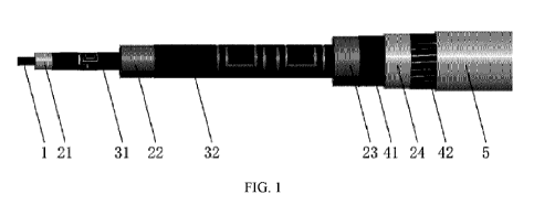
[00100] As shown in FIG. 1, the filtering cable provided in this embodiment
sequentially
comprises a core wire 1, a first filling layer 21 surrounding the core wire 1,
a first defective
conductor layer 31, a second filling layer 22, a second defective conductor
layer 32, a third
filling layer 23, a first shielding layer 41, a fourth filling layer 24, a
second shielding layer 42,
and an outer sheath 5 from inside to outside in the cross section in the
radial direction of the
filtering cable. The structure of a filtering cable shown in FIG. 1 is only an
example, and is not
Date Recue/Date Received 2020-10-20
limited, and other structures may also be used.
[00101] As shown in FIGS. 2, 3 and 4, the first defective conductor layer 31
etches a
periodically or non-periodically etching pattern 312 of a first defective
conductor layer on the
conductor 311 of the first defective conductor layer on the cylindrical
surface of the first filling
layer 21, and the etched part may be hollow or filled with insulating material
in situ. In this
embodiment, as shown in FIG. 4, the etching pattern 312 obtained by
periodically etching a part
of the first defective conductor layer on the cylindrical surface of the
conductor 311 of the first
defective conductor layer comprises a spiral etching pattern. Specifically,
the etching pattern
comprises: a plurality of first patterns; in FIG. 4, the first pattern
comprises: a first hollow line
segment 601 provided in the radial direction of the filtering cable, one end
of the first hollow
line segment 601 is provided with a first spiral hollow pattern 602, and the
other end is provided
with a second spiral hollow pattern 603; the second spiral hollow pattern 603
and the first spiral
hollow pattern 601 are provided symmetrically. Based on this, as shown in FIG.
5, the etching
pattern of the first defective conductor layer 31 can make the filtering cable
equivalent circuit to
be: the transmission line intrinsic impedance ZO (the equivalent electric
length (p) between the
first node Pi and the second node P2 is connected in parallel with a short-
circuit short-harmonic
line with the impedance Z2 and the equivalent electrical length 0, the
impedance Zi and the
equivalent electrical length 20, and the impedance Z2 and the equivalent
electrical length 0,
and is connected in parallel with the first inductor Li and the first resistor
Ri.
[00102] The first node is the input terminal of the filtering cable, the
second node is the
output terminal of the filtering cable, and the equivalent circuit between the
first node Pi and the
second node P2 varies with the etching pattern.
[00103] The second filling layer 22 tightly wraps the first defective
conductor layer 31 to
form a cylindrical structure together. Specifically, the second filling layer
22 is uniformly
wrapped outside the first defective conductor layer 31 using an insulating
material such as
polytetrafluoroethylene or polyethylene by winding or extrusion foaming.
[00104] As shown in FIGS. 6, 7 and 8, the second defective conductor layer 32
etches a
periodically or non-periodically etching pattern 322 of a first defective
conductor layer on the
conductor 321 of the second defective conductor layer on the cylindrical
surface of the second
filling layer 22, and the etched part may be hollow or filled with insulating
material such as
polytetrafluoroethylene or polyethylene in situ. In this embodiment, the
etching pattern 322
obtained by periodically etching a part of the second defective conductor
layer on the
cylindrical surface of the conductor 321 of the second defective conductor
layer is shown in
FIG. 8. The etching pattern comprises: a plurality of second patterns; in FIG.
8, the second
16
Date Recue/Date Received 2020-10-20
patterns comprise: a first double-ring hollow pattern 604 and a second double-
ring hollow
pattern 605 spaced from each other; the first double-ring hollow pattern 604
and the second
double-ring hollow pattern 605 are symmetrical and the axis of symmetry is
provided in the
radial direction of the filtering cable; the first double-ring hollow pattern
604 and the second
double-ring hollow pattern 605 have a first non-hollow area 606 at the middle
of the side of the
outer ring close to the axis of symmetry; the first double-ring hollow pattern
604 and the second
double-ring hollow pattern 605 have a second non-hollow area 607 at the middle
of the side of
the inner ring away from the axis of symmetry.
[00105] There are various shapes of the first double-ring hollow
patterns 604 and the
second double-ring hollow patterns 605, which may be, but not limited to,
rectangular, which
are illustrated by rectangles in the figure.
[00106] The second defective conductor layer 32 can make the filtering cable
equivalent to
the equivalent circuit shown in FIG. 9. The equivalent circuit in FIG. 9
comprises a second
inductor L2, a third inductor L3, a fourth inductor La, a fifth inductor Ls, a
sixth inductor L6, a
seventh inductor L7, a first capacitor Ci, a second capacitor C2, a third
capacitor C3, a fourth
capacitor C4, a fifth capacitor Cs, a sixth capacitor C6, and a seventh
capacitor C7. The first end
of the second inductor L2 is connected to the first node Pi and the first end
of the first capacitor
Cl, respectively, and the second end of the second inductor L2 is connected to
the first end of
the third inductor L3 and the first end of the second capacitor C2,
respectively; the second end of
the third inductor L3 is connected to the first end of the fourth inductor La
and the first end of
the fourth capacitor C4, respectively; the second end of the fourth inductor
La is connected to
the first end of the fifth inductor Ls and the first end of the fifth
capacitor Cs, respectively, and
the second end of the fifth inductor Ls is connected to the first end of the
seventh capacitor C7
and the second node P2, respectively. The second end of the second capacitor
C2 is connected to
the first end of the sixth inductor L6 and the first end of the third
capacitor C3, respectively; the
second end of the fifth capacitor Cs is connected to the first end of the
seventh inductor L7 and
the first end of the sixth capacitor C6, respectively; the second end of first
capacitor Ci, the
second end of the sixth inductor L6, the second end of third capacitor C3, the
second end of
fourth capacitor C4, the second end of seventh inductor L7, the second end of
the sixth capacitor
C6 and the second end of the seventh capacitor C7 are all grounded.
[00107] The third filling layer 23 tightly wraps the second defective
conductor layer 32 to
form a cylindrical structure together. Specifically, the third filling layer
23 is uniformly wrapped
outside the second defective conductor layer using an insulating material such
as
polytetrafluoroethylene or polyethylene by winding or extrusion foaming.
17
Date Recue/Date Received 2020-10-20
[00108] The first shielding layer 41 wraps one or more metal shielding
layers outside the
third insulating layer 23. For example, the first shielding layer is a silver-
plated copper tape.
[00109] The fourth insulating layer 24 tightly wraps the first
shielding layer 41 to form a
cylindrical structure. For example, the material of the fourth filling layer
comprises fluorinated
ethylene propylene polymer.
[00110] The second shielding layer 42 wraps one or more metal shielding layers
on the
outside of the fourth insulating layer 24. For example, the second shielding
layer is an
ultra-light silver-plated metal braided layer or a silver-plated copper
braided mesh.
[00111] The first defective conductor layer 31, the second defective
conductor layer 32, the
first shielding layer 41, and the second shielding layer 42 may be connected
together as needed
to form a common ground connection.
[00112] As shown in FIG. 10, from the insertion loss effect diagram achieved
by the
filtering cable based on the defective conductor layer in this embodiment, it
can be seen that the
filtering cable based on the defective conductor layer is a low-pass filtering
cable. The insertion
.. loss effect achieved by the filtering cable based on the defective
conductor layer with the length
of 0.1 m is as follows: the insertion loss at 0-2GHz is less than 0.5dB, and
the insertion loss at
2.2-8GHz is greater than 30dB. In FIG. 10, the abscissa represents frequency
in units of GHz
(i.e., GH), and the ordinate represents insertion loss in units of dB (i.e.,
difference loss).
[00113] In specific implementation, etching patterns of various
structures can be designed
according to actual needs to achieve the various required effects of the
filter circuit. In a
possible design, the preset filter circuit may comprise a low-pass filter
circuit, a band-stop filter
circuit, or a band-pass filter circuit. The structure of different etching
patterns is exemplified
hereinafter.
[00114] Structure one:
[00115] If the value of N is 1, and the preset filter circuit comprises a
low-pass filter
circuit, the etching pattern comprises: a plurality of third patterns.
[00116] As shown in FIGS. 11 and 12, FIG. 12 shows a specific structure of one
period of
the etching pattern (the third pattern shown by the dotted frame A). The third
patterns comprise:
a second hollow line segment 608 in the axial direction of the filtering
cable; the second hollow
line segment 608 comprises a third hollow line segment 609, a fourth hollow
line segment 610
and a fifth hollow line segment 611 which are symmetrical at both ends of the
third hollow line
segment and in which the axis of symmetry is provided along the diameter of
the filtering cable;
a sixth hollow line segment 612 that is spaced side by side with the second
hollow line segment
18
Date Recue/Date Received 2020-10-20
608; an area on the sixth hollow line segment 612 corresponding to the third
hollow line
segment 609 has a third non-hollow area 613, the area on the sixth hollow line
segment 612
corresponding to the fourth hollow line segment 610 has a first narrowed
hollow area 614
communicated with the fourth hollow line segment 610, and the area on the
sixth hollow line
segment 612 corresponding to the fifth hollow line segment 611 has a second
narrowed hollow
area 615 communicated with the fifth hollow line segment 611, wherein the
width of the first
narrowed hollow area 614 and the second narrowed hollow area 615 in the radial
direction of
the filtering cable is smaller than the width of other positions on the sixth
hollow line segment
612.
[00117] This embodiment provides a low-pass filtering cable based on an
asymmetric PI
(i.e., 70-shaped defective conductor layer, as shown in FIG. 11. In specific
implementation, a
copper layer with 10 cascaded asymmetric PI-shaped third patterns can be
constructed on a
polyimide film substrate and is wrapped around the insulating layer of the
filtering cable, which
realizes the low-pass filtering function of the filtering cable. The third
pattern in FIG. 12 is a
structural diagram of a resonance unit A. Typical values of the structural
parameters are as
follows: the relative dielectric constant of the polyimide film substrate is
Er = 3.8, the loss
tangent is tans = 0.008, and the substrate size is length Lsub x width Wsub x
height Hsub =
100mm x 2.6mm x 0.254mm. The size of the resonance unit is as follows: the
length of the
second hollow line segment 608 in the axial direction of the filtering cable
is Di = 9.3mm, the
period interval distance of the third pattern is D2 = 0.7mm, the length of the
fourth hollow line
segment 610 in the axial direction of the filtering cable is D3 = 3.9mm, the
length of the area of
the first narrowed hollow 614 for communication and the area of the second
narrowed hollow
area 615 for communication in the axial direction of the filtering cable is at
= 0.3mm, the
length on the sixth narrowed line segment 612 located between the first
narrowed hollow area
614 and the third non-hollow area 613 and the length on the sixth hollow line
segment 612
located between the second narrowed hollow area 615 and the third non-hollow
area 613 are D5
= 1.5mm, the diameter of the filtering cable insulating layer is Dr = 1.07mm,
the diameter of the
inner conductor is Di = 0.5mm. The length of the second hollow line segment
608 in the radial
direction of the filtering cable is Wi = 0.465mm, the distance between both
sides of the second
.. hollow line segment 608 close to the sixth hollow line segment 612 is W2 =
lmm, the line width
of the first narrowed hollow area 614 and the second narrowed hollow area 615
is narrower than
the line width of other positions on the sixth hollow line segment 612 by W3 =
0.4mm, the
distance between both sides of the second hollow line segment 608 away from
the sixth hollow
line segment 612 is W4=1.965mm, and the side of the sixth hollow line segment
612 away from
the second hollow line segment 608 has at least a length W5 = 0.45 mm of the
non-hollow area
19
Date Recue/Date Received 2020-10-20
in the radial direction of the filtering cable. The parameters Di and D3
become larger, which can
reduce the frequency of response. If the radius of the filtering cable is
small, the resonant
frequency of the filter is lower and the effect becomes better. The filtering
cable implemented
by the structure of this embodiment has a strong transition band (TB), an
ultra-wide stop-band
(SB) and a very high stop-band performance. The defective conductor layer with
10 cascaded
resonance units provided in this embodiment has a compact size of 100mm x
2.6mm x
0.254mm, the insertion loss is less than 1.9dB at 2.2GHz, and a wide SB
greater than 50dB is
provided in the range of 2.7GHz to 12GHz. The flexible low-pass filtering
cable proposed in
this embodiment has a function of good transmission and low-pass filtering,
and it is possible to
replace traditional RF coaxial cables in wireless terminals.
[00118] Structure two:
[00119] If the value of N is 1, and the preset filter circuit comprises
a low-pass filter
circuit, the etching pattern comprises: a plurality of fourth patterns.
[00120] As shown in FIG. 13, the fourth patterns comprise: two sub-patterns
616 which are
symmetrically spaced from each other and in which the axis of symmetry is
provided in the
radial direction of the filtering cable. The sub-patterns 616 of the fourth
pattern comprise a
seventh hollow line segment 617 and an eighth hollow line segment 618 provided
side by side
in the radial direction of the filtering cable; both ends of the seventh
hollow line segment 617
are provided with a first single-ring hollow pattern 619, respectively; the
middle of the side of
the first single-ring hollow pattern 619 away from the seventh hollow line
segment 617 is
provided with a non-hollow area; both ends of the eighth hollow line segment
618 are provided
with a second single-ring hollow pattern 620, respectively; the middle of the
side of the second
single-ring hollow pattern 620 away from the eighth hollow line segment 618 is
provided with a
non-hollow area; the area surrounded by the second single-ring hollow pattern
620 is larger than
.. the area surrounded by the first single-ring hollow pattern 619, wherein
the widths of the
corresponding hollow line segments of the first ring hollow pattern 619 and
the second ring
hollow pattern 620 are the same. The widths of the seventh hollow line
segment, the eighth
hollow line segment, the non-hollow area of the first ring hollow pattern and
the non-hollow
area of the second ring hollow pattern in the axial direction of the filtering
cable are the same.
.. [00121] It can be seen from FIG. 13 that the fourth pattern is very similar
to a dumbbell
structure as a whole. It can be considered that the defective conductor layer
of the low-pass
filtering cable provided in this embodiment embeds a T-shaped region on the
basis of the
dumbbell-shaped structure. The two transmission zeros produced by the new
defective
conductor layer structure are both lower than those produced by etching a
dumbbell-shaped
Date Recue/Date Received 2020-10-20
defective conductor layer of the same square area size. During implementation,
the shapes of
the second single-ring hollow pattern 620 and the first single-ring hollow
pattern 619 may be,
but not limited to, rectangular, which are illustrated by rectangles in the
figure. The
corresponding size can be set according to actual needs. For example, the size
of the structure
shown in FIG. 13 is as follows: the axial length of the outer ring of the
first single-ring hollow
pattern 619 is D6 = 5mm, the distance between the first single-ring hollow
pattern 619 and the
second single-ring hollow pattern 620 is D7 = 6mm, the width of the outer ring
of the second
single-ring hollow pattern 620 is Ds = 8mm, the distance between the second
single-ring hollow
patterns 620 of the two sub-patterns is D9 = 6mm, the length of the inner ring
of the first
single-ring hollow pattern 619 in the axial direction of the filtering cable
is Dio = 4mm, the
length of the inner ring of the second single-ring hollow pattern 620 in the
axial direction of the
filtering cable is Dii = 7mm, the length of the outer ring of the first single-
ring hollow pattern
619 in the radial direction of the filtering cable is W6 = 3mm, the length of
the outer ring of the
second single-ring hollow pattern 620 in the radial direction of the filtering
cable is W7 = 5mm,
the length of one side of the first single-ring hollow pattern 619 with a non-
hollow area in the
radial direction of the filtering cable is Ws = 1 mm, the length of one side
of the second
single-ring hollow pattern 620 with a non-hollow area in the radial direction
of the filtering
cable is W9 = imm, the length of the inner ring of the first single-ring
hollow pattern 619 in the
radial direction of the filtering cable is Wio = 1.5mm, the length of the
inner ring of the second
single-ring hollow pattern 620 in the radial direction of the filtering cable
is Wii = 3.5mm, the
length of the seventh hollow line segment and the eighth hollow line segment
in the radial
direction of the filtering cable is Wi2= 1.5mm, and the width of the seventh
hollow line segment
in the radial direction of the filtering cable gi = the width of the eighth
hollow line segment in
the radial direction of the filtering cable g2 = the length of the non-hollow
area provided in the
first single-ring hollow pattern 619 in the radial direction of the filtering
cable g3 = the length of
the non-hollow area provided in the second single-ring hollow pattern 620 in
the radial direction
of the filtering cable ga = 0.4mm. The structure of this embodiment can make
the filtering cable
equivalent to the equivalent circuit shown in FIG. 14. The equivalent circuit
shown in FIG. 14
comprises a second resistor R2, an eighth capacitor Cs, a ninth capacitor C9,
a tenth capacitor
cio, an eleventh capacitor Cii, an eighth inductor Ls, and a ninth inductor
L9. The first end of
the second resistor R2 is connected to the first node Pi, the first end of the
eighth inductor Ls,
the first end of the eighth capacitor Cs, and the first end of the ninth
capacitor C9, respectively,
and the second end thereof is connected to the second nodes P2, the second end
of the eighth
inductor Ls, the second end of the eighth capacitor Cs, and the first end of
the tenth capacitor
cio, respectively; the second end of the ninth capacitor C9 is connected to
the first end of the
21
Date Recue/Date Received 2020-10-20
eleventh capacitor C11, the first end of the ninth inductor L9 and the second
end of the tenth
capacitor Cio, respectively; the second end of the eleventh capacitor Cii and
the second end of
the ninth inductor L9 are both grounded. The filtering performance based on
this structure
comprises: obtaining a low-pass filter with a cutoff frequency of 3 dB,
showing a very sharp
cutoff frequency response and an ultra-wide stop-band at 4 GHz, and having the
suppression at
4.2 to 23 GHz higher than 25 dB.
[00122] Structure three:
[00123] If the value of N is 1, and the preset filter circuit comprises
a low-pass filter
circuit, the etching pattern comprises: a plurality of fifth patterns. As
shown in FIG. 15, the fifth
patterns comprise: a ninth hollow line segment 621 and a tenth hollow line
segment 623 that are
provided crosswise; the ninth hollow line segment 621 is provided in the axial
direction of the
filtering cable and is provided with a first widened hollow area 622 at both
ends; the tenth
hollow line segment 623 is provided in the radial direction of the filtering
cable and is provided
with a second widened hollow area 624 at both ends; an area surrounded by the
second widened
hollow area 623 is larger than the area surrounded by the first widened hollow
area 622.
[00124] This embodiment provides a low-pass filtering cable based on a crossed
dumbbell-shaped defective conductor layer. As can be seen from FIG. 15, the
low-pass filtering
cable based on a crossed dumbbell-shaped defective conductor layer implements
the low-pass
filtering function by two cross-shaped dumbbell-shaped structures, which can
achieve higher
stop-band suppression and wider band stop-band characteristics than dumbbell-
shaped
structures. Based on the structure of FIG. 15, specific parameters can be set
according to actual
needs. For example, in some embodiments, the specific parameters are as
follows: the length of
the second widened hollow area 624 in the axial direction of the filtering
cable is W13 = 12 mm,
the length of the first widened hollow area 622 in the axial direction of the
filtering cable is Wm
.. = 3mm, the length of the tenth hollow section 623 in the axial direction of
the filtering cable
Wis = the length of the ninth hollow section 621 in the radial direction of
the filtering cable W16
= 2mm, the length of the second widened hollow area 624 in the radial
direction of the filtering
cable is W17 = 5mm, and the length of the first widened hollow area 622 in the
radial direction
of the filtering cable is Wis = 5mm. The structure of this embodiment can make
the filtering
cable equivalent to the equivalent circuit shown in FIG. 16. The circuit in
FIG. 16 comprises a
tenth inductor Lio, an eleventh inductor Lii, a twelfth inductor Li2, a
thirteenth inductor L13, a
fourteenth inductor Li4, a fifteenth inductor Lis, a twelfth capacitor Ci2, a
thirteenth capacitor
C13, a fourteenth capacitor C14, a fifteenth capacitor Cis, a sixteenth
capacitor C16, a seventeenth
capacitor C17, and a eighteenth capacitor Cis. The first end of the tenth
inductor Lio is connected
22
Date Recue/Date Received 2020-10-20
to the first node Pi and the first end of the twelfth capacitor C12,
respectively, and the second
end thereof is connected to the first end of the thirteenth capacitor C13, the
first end of the
eleventh inductor Lii, and the first end of the fourteenth capacitor C14; the
second end of the
eleventh inductor Lii is connected to the second end of the fourteenth
capacitor C14 and the first
end of the twelfth inductor L12, respectively; the second end of the twelfth
inductor Li2 is
connected to the first end of the thirteenth inductor L13 and the first end of
the fifteenth capacitor
Cis, respectively; the second end of the thirteenth inductor L13 is connected
to the first end of
the fourteenth inductor Li4 and the first end of the sixteenth capacitor C16,
respectively; the
second end of the fourteenth inductor Li4 is connected to the second end of
the sixteenth
capacitor C16, the first end of the fifteenth inductor Lis, and the first end
of the seventeenth
capacitor C17, respectively; the second end of the fifteenth inductor Lis is
connected to the
second node P2 and the first end of the eighteenth capacitor C18,
respectively; the second end of
the twelfth capacitor C12, the second end of the thirteenth capacitor C13, the
second end of the
fifteenth capacitor Cis, the second end of the seventeenth capacitor C17, and
the second end of
the eighteenth capacitor Cis are grounded, respectively. The filtering
performance based on this
structure comprises: insertion loss from DC to 3.5GHz less than 2dB, and
suppression from 4.3
to 15.8GHz higher than 20dB.
[00125] Structure four:
[00126] If the value of N is 1, and the preset filter circuit comprises
a low-pass filter
circuit, the etching pattern comprises: a plurality of sixth patterns; as
shown in FIG. 17, the
sixth patterns comprise: a first U-shaped hollow pattern 625, a second U-
shaped hollow pattern
626, and a third U-shaped hollow pattern 627 that are sequentially provided;
the openings of the
first U-shaped hollow pattern 625, the second U-shaped hollow pattern 626 and
the third
U-shaped hollow pattern 627 are provided in the radial direction of the
filtering cable; wherein
the opening direction of the second U-shaped hollow pattern 626 is opposite to
the opening
direction of the first U-shaped hollow pattern 625 and the third U-shaped
hollow pattern 627;
one end of the second U-shaped hollow pattern 626 is communicated with one end
of the first
U-shaped hollow pattern 625, and the other end thereof is communicated with
one end of the
third U-shaped hollow pattern 627. The sizes of the first U-shaped hollow
pattern 625, the
second U-shaped hollow pattern 626, and the third U-shaped hollow pattern 627
may be the
same.
[00127] The sixth pattern is very much like a W as a whole. It can be
considered that this
embodiment provides a low-pass filtering cable based on a W-type defective
conductor layer. As
can be seen from FIG. 17, the low-pass filtering cable based on a W-type
defective conductor
23
Date Recue/Date Received 2020-10-20
layer realizes the low-pass filtering function through the structure similar
to W, which can
realize three transmission zeros, sharp roll-off and wider stop-band
characteristics. The specific
parameters of the structure shown in FIG. 17 are as follows: the length of the
sixth pattern in the
radial direction of the filtering cable is Diz = 5mm, the length of one end of
the U-shaped
hollow pattern in the axial direction of the filtering cable D13 = the length
of the other end of the
U-shaped hollow pattern in the axial direction of the filtering cable D14 =
0.2mm, the distance
between both ends of the U-shaped hollow pattern is Dis = 1.4mm, the length of
the U-shaped
hollow pattern in the radial direction of the filtering cable W19 = 1 3.64mm,
the length of one
end of the U-shaped hollow pattern in the radial direction of the filtering
cable is W21, and the
length of the other end thereof in the radial direction of the filtering cable
is Wzo = 7.76mm. The
structure of this embodiment can make the filtering cable equivalent to the
equivalent circuit
shown in FIG. 18. The equivalent circuit in FIG. 18 comprises a sixteenth
inductor L16, a
seventeenth inductor L17, a eighteenth inductor Lis, a nineteenth inductor
L19, a nineteenth
capacitor C19, a twentieth capacitor C20, a twenty-first capacitor C21, a
twenty-second capacitor
Czz, a twenty-third capacitor C23, a twenty-fourth capacitor C24, a twenty-
fifth capacitor C25, a
twenty-sixth capacitor C26, a twenty-seventh capacitor C27, and a twenty-
eighth capacitor C28.
The first end of the sixteenth inductor L16 is connected to the first end of
the first node Pi and
the nineteenth capacitor C19, respectively, and the second end thereof is
connected to the second
node Pz and the first end of the twenty-second capacitor Czz, respectively;
the second end of the
nineteenth capacitor C19 is connected to the first end of the twentieth
capacitor Czo and the first
end of the twenty-third capacitor C23, respectively; the second end of the
twentieth capacitor Czo
is connected to the first end of the twenty-first capacitor C21 and the first
end of the
twenty-fourth capacitor C24, respectively; the second end of the twenty-first
capacitor C21 is
connected to the second end of the twenty-second capacitor Czz and the first
end of the
twenty-fifth capacitor C25, respectively; the second end of the twenty-third
capacitor C23 is
connected to the first end of the twenty-sixth capacitor C26 and the first end
of the seventeenth
inductor L17, respectively; the second end of the twenty-fourth capacitor Cza
is connected to the
first end of the twenty-seventh capacitor C27 and the first end of the
eighteenth inductor Lis,
respectively; the second end of the twenty-fifth capacitor C25 is connected to
the first end of the
twenty-eighth capacitor C28 and the first end of the nineteenth inductor L19,
respectively; the
second end of the twenty-sixth capacitor C26, the second end of the
seventeenth inductor L17, the
second end of the twenty-seventh capacitor C27, the second end of the
eighteenth inductor L18,
the second end of the twenty-eighth capacitor C28 and the second end of the
nineteenth inductor
L19 are grounded, respectively. The filtering performance achieved based on
the above structure
comprises: the transition band is from 3.11 GHz (which is the cutoff
frequency) to 3.23 GHz,
24
Date Recue/Date Received 2020-10-20
the insertion loss changes from -3.02 dB to -22.5 dB; the insertion loss of
the stop-band is 25
dB, and the frequency band of the stop-band can be extended to 3.4GHz (which
is the cutoff
frequency).
[00128] Structure five:
[00129] If the value of N is 1, and the preset filter circuit comprises a
low-pass filter
circuit, the etching pattern comprises: a plurality of seventh patterns; as
shown in FIG. 19, the
seventh patterns comprise: an eleventh hollow line segment 628 in the radial
direction of the
filtering cable; both ends of the eleventh hollow line segment 628 are
provided with a third
widened hollow area 629, respectively. The length of the third widened hollow
area 629 in the
.. axial direction of the filtering cable is greater than the length of other
areas of the eleventh
hollow line segment 628 in the axial direction of the filtering cable, which
looks like a
dumbbell.
[00130] This embodiment provides a low-pass filtering cable based on a
dumbbell-shaped
defective conductor layer. As can be seen from FIG. 19, in this embodiment,
the low-pass
filtering cable based on a dumbbell-shaped defective conductor layer realizes
the low-pass
filtering function through a dumbbell-like (or I-type) structure, which can
realize sharp roll-off
and wider stop-band characteristics. The specific parameters of the structure
shown in FIG. 19
are as follows: the length of the third widened hollow region 629 in the axial
direction of the
filtering cable is D16 = 2.5mm, the length of the eleventh hollow line segment
628 in the axial
.. direction of the filtering cable is D17 = 0.5mm, the length of the third
widened hollow area 629
in the radial direction of the filtering cable is W22 = 2.6mm, and the length
of the eleventh
hollow section 628 in the radial direction of the filtering cable is W23 =
2.0mm. The structure of
this embodiment can make the filtering cable equivalent to the equivalent
circuit shown in FIG.
20. The equivalent circuit in FIG. 20 comprises a twentieth inductor Lzo and a
twenty-ninth
capacitor C29. The first end of the twentieth inductor Lzo is connected to the
first node Pi and the
first end of the twenty-ninth capacitor C29, respectively, and the second end
thereof is
connected to the second node P2 and the second end of the twenty-ninth
capacitor C29,
respectively. The filtering performance based on this structure comprises: the
transition band is
from the pass-band as DC to 4GHz, the insertion loss is less than 0.2dB, and
the stop-band is
from 4.3GHz to 16.2GHz.
[00131] Structure six:
[00132] If the value of N is 1, and the preset filter circuit comprises
a band-stop filter
circuit, the etching pattern comprises: a plurality of eighth patterns; as
shown in FIG. 21, the
eighth patterns comprise: a twelfth hollow line segment 630 in the radial
direction of the
Date Recue/Date Received 2020-10-20
filtering cable; both ends of the twelfth hollow line segment 630 are provided
with a third
single-ring hollow pattern 631, respectively; the third single-ring hollow
pattern 631 has a
non-hollow area 632 on the side close to the twelfth hollow line segment 630,
wherein the third
single-ring hollow pattern 631 may be, but not limited to, a ring hollow
pattern.
[00133] This embodiment provides a band-stop filtering cable based on a double-
ring
bridge-connected defective conductor layer. As can be seen from the figure,
the band-stop
filtering cable based on a double-ring bridge-connected defective conductor
layer realizes the
band-stop filtering function through two etched ring-shaped groove and a
narrow etching gap
bridge-connected structure. The specific parameters of the structure of this
embodiment are as
follows: the length of the twelfth hollow line segment 630 in the axial
direction of the filtering
cable W24 = the width of the ring-shaped line of the third single-ring hollow
pattern 631 W25 =
0.4 mm, the length of the non-hollow area of the third single-ring hollow
pattern 631 is Si =
0.2mm, the radius of the outer ring of the third single-ring hollow pattern 63
us R = 4mm, and
the length of the twelfth hollow line segment 630 in the radial direction of
the filtering cable is
Di8= 2mm. The structure of this embodiment can make the filtering cable
equivalent to the
equivalent circuit shown in FIG. 22. The circuit of FIG. 22 comprises a twenty-
first inductor
L2i, a twenty-second inductor L22, a third resistor R3, a thirty capacitor
C30, a thirty-first
capacitor C31, and a thirty-second capacitor C32. The first end of the twenty-
first inductor L21 is
connected to the first node Pi and the first end of the thirtieth capacitor
C30, respectively, and the
.. second end thereof is connected to the third resistor R3, the first end of
the twenty-second
inductor L22, and the first end of the thirty-first capacitor C31,
respectively; the second end of the
third resistor R3 is connected to the second node P2, the second end of the
twenty-second
inductor L22, the second end of the thirty-first capacitor C31, and the first
end of the
thirty-second capacitor C32, respectively; the second end of the thirtieth
capacitor C30, and the
second end of the thirty-second capacitor C32 are grounded, respectively. The
filtering
performance based on this structure comprises: in the case of a single
resonance unit, obtaining
the stop-band insertion loss of 1.5GHz-1.6GHz greater than 20dB, and in the
case of cascading,
greatly improving the stop-band insertion loss. The insertion loss in the pass-
band of
DC-1.4GHz, 1.7GHz-4GHz is small, less than ldB.
.. [00134] Structure seven:
[00135] If the value of N is 1, and the preset filter circuit comprises
a band-stop filter
circuit, the etching pattern comprises: a plurality of ninth patterns; as
shown in FIG. 23, the
ninth patterns comprise: a thirteenth hollow line segment 633 provided in the
radial direction of
the filtering cable, a third spiral hollow pattern 634 is provided at one end
of the thirteenth
26
Date Recue/Date Received 2020-10-20
hollow line segment 633, and a fourth spiral hollow pattern 635 is provided at
the other end
thereof; the third spiral hollow pattern 634 is asymmetrical with the fourth
spiral hollow pattern
635.
[00136] This embodiment provides a dual-band band-stop filtering cable based
on an
asymmetric bridge-connected spiral defective conductor layer. As shown in FIG.
23, the
band-stop filtering cable based on an asymmetric bridge-connected spiral
defective conductor
layer realizes the dual-band band-stop filtering function through two etched
asymmetric spiral
gaps and a narrow etching gap bridge-connected structure. The specific
parameters of the
structure shown in FIG. 23 are as follows: the length of the thirteenth hollow
line segment 633
in the axial direction of the filtering cable is W26 = 0.2mm, the pitch of the
third spiral hollow
pattern and the pitch of the fourth spiral hollow pattern are both Sz = 0.2mm,
the length of the
thirteenth hollow section 633 in the radial direction of the filtering cable
is D19 = 2.4mm, the
length of the third spiral hollow pattern 634 in the axial direction of the
filtering cable is Dzo =
3.2mm, the length of the third spiral hollow pattern 634 in the radial
direction of the filtering
cable is Dzi = 3.0 mm, the length of the fourth spiral hollow pattern 635 in
the radial direction
of the filtering cable is D22 = 2.4 mm, and the length of the fourth spiral
hollow pattern 635 in
the axial direction of the filtering cable is D23 = 2.6 mm. The structure of
this embodiment can
make the filtering cable equivalent to the equivalent circuit shown in FIG.
24. The equivalent
circuit in FIG. 24 comprises: a fourth resistor Ita, a fifth resistor R5, a
twenty-third inductor L23,
a twenty-fourth inductor L24, a thirty-third capacitor C33, and a thirty-
fourth capacitor C34. The
first end of the fourth resistor Ita is connected to the first node Pi, the
first end of the
twenty-third inductor L23, and the first end of the thirty-third capacitor
C33, and the second end
thereof is connected to the second end of the twenty-third inductor L23, the
second end of the
thirty-third capacitor C33, the first end of the fifth resistor R5, the first
end of the twenty-fourth
inductor L24, and the first end of the thirty-fourth capacitor C34; the second
end of the fifth
resistor R5 is connected to the second end of the twenty-fourth inductor L24,
the second end of
the thirty-fourth capacitor C34, and the second node Pz. The filtering
performance based on this
structure comprises: in the case of a single resonance unit, obtaining two
stop-bands of 3.0 GHz
and 4.5 GHz with the insertion loss of the stop-band greater than 20 dB, and
in the case of
cascading, greatly improving the stop-band insertion loss. The insertion loss
in the pass-band of
DC-2.7GHz, 3.2GHz-4.3GHz, and 4.7GHz-6GHz is small, less than 1 dB.
[00137] Structure eight:
[00138] If the value of N is 1, and the preset filter circuit comprises
a band-stop filter
circuit, the etching pattern comprises: a plurality of tenth patterns; as
shown in FIG. 25, the
27
Date Recue/Date Received 2020-10-20
tenth patterns comprise: a fourteenth hollow line segment 636 and a fifteenth
hollow line
segment 637 spaced side by side in the axial direction of the filtering cable;
a sixteenth hollow
line segment 638 provided between the fourteenth hollow line segment 636 and
the fifteenth
hollow line segment 637 in the radial direction of the filtering cable; the
middle of the
fourteenth hollow line segment 636 is communicated with the middle of the
fifteenth hollow
line segment 637 through the sixteenth hollow line segment 638; a third single-
ring hollow
pattern 639 is provided between the fourteenth hollow line segment 636 and the
fifteenth hollow
line segment 637 and at both sides of the sixteenth hollow line segment 638;
the middle of the
side of the third single-ring hollow pattern 639 close to the sixteenth hollow
line segment 638 is
provided with a non-hollow area.
[00139] The tenth pattern is very much like a symmetrical H and two Cs. It can
be
considered that this embodiment provides a band-stop filtering cable based on
a symmetrical H
and C-shaped defective conductor layer, as shown in FIG. 25, the band-stop
filtering cable
based on a symmetrical H and C-shaped defective conductor layer is closely
placed between
two opposing C-shaped gaps through an H-shaped gap, forming a mutually coupled
resonator to
realize the band-stop filtering function, which can significantly reduce the
common mode noise
without affecting the differential signal. The specific parameters of the
structure shown in FIG.
are as follows: the lengths of the fourteenth hollow line segment 636 and the
fifteenth hollow
line segment 637 in the radial direction of the filtering cable are both Dza =
6.375mm, the length
20 of the third single-ring hollow pattern 639 in the radial direction of
the filtering cable is D25 =
2.55mm, the length of the side of the third single-ring hollow pattern 639
close to the sixteenth
hollow line segment 638 in the axial direction of the filtering cable is D26 =
1.275mm, the
length of the tenth pattern in the radial direction of the filtering cable is
W27 = 6.375mm, the
length of the outer ring of the third single-ring hollow pattern 639 in the
radial direction of the
25 filtering cable is W28 = 4.76mm, the length of the inner ring of the
third single-ring hollow
pattern 639 in the radial direction of the filtering cable is W29 = 3.4mm, the
distance between
the non-hollow area of the third single-ring hollow pattern 639 and the non-
hollow area of the
side of the fourteenth hollow line segment 636 close to the third single-ring
hollow pattern 639
is W3o= 2.04mm, the length of the sixteenth hollow line segment 638 in the
radial direction of
the filtering cable is S3 = 0.255mm, the length of the side of the third
single-ring hollow pattern
639 away from the sixteenth hollow line segment 638 in the axial direction of
the filtering cable
is Sa = 0.3mm, the length of the fourteenth hollow line segment 636 and the
fifteenth hollow
line segment in the radial direction of the filtering cable is S5 = 0.2mm. The
filtering
performance based on this structure comprises: in the case of a single
resonance unit, obtaining
a stop-band with the center frequency of 8.4 GHz, the cutoff frequency of 6.2
GHz, and the
28
Date Recue/Date Received 2020-10-20
bandwidth of 73.8%. The common mode insertion loss in the stop-band is not
less than 15dB,
and the differential mode insertion loss is not more than 3dB.
[00140] Structure nine:
[00141] If the value of N is 1, and the preset filter circuit comprises
a band-stop filter
circuit, the etching pattern comprises: a plurality of eleventh patterns; as
shown in FIG. 26, the
eleventh patterns comprise: a rectangular fourth single-ring hollow pattern
640; one pair of
sides of the fourth single-ring hollow pattern 640 are provided in the radial
direction of the
filtering cable, and the other pair of sides thereof is provided in the axial
direction of the
filtering cable; a seventeenth hollow line segment 641 is provided outside the
fourth single-ring
hollow pattern, and at both ends of and the middle of one pair of sides
provided in the axial
direction of the filtering cable, respectively; one end of the seventeenth
hollow line segment 641
is communicated with the fourth single-ring hollow pattern 640; two symmetric
L-shaped
hollow patterns 642 are provided between the two seventeenth hollow line
segments 641; the
corner of the L-shaped hollow pattern 642 is close to the fourth single-ring
hollow pattern, one
side thereof is close to the seventeenth hollow line segment 641, is provided
in the radial
direction of the filtering cable, and is communicated with the close
seventeenth hollow line
segment 641 through the hollow line segment which is provided in the axial
direction of the
filtering cable, and the other side thereof is close to the fourth single-ring
hollow pattern 640
and is provided in the axial direction of the filtering cable; the area of the
core wire
corresponding to the fourth single-ring hollow pattern 640 is provided with a
through-hole 643
in the radial direction of the filtering cable.
[00142] This embodiment provides a band-stop filtering cable based on a
symmetric
L-shaped defective conductor layer. As shown in FIG. 26, the band-stop
filtering cable based on
a symmetric L-type defective conductor layer realizes the band-stop filtering
function in such a
way that 4 pairs of L-shaped gaps symmetrically distributed about the center
line form mutually
coupled resonators. In order to obtain a better band-stop response, the cable
core is used to
realize the band-stop characteristic through electromagnetic coupling, but the
coupling is very
weak. Therefore, in order to increase the coupling between the cable core wire
and the defective
conductor layer, a periodic metal via connection is introduced to produce an
improved coupling
between the core wire and the defective conductor layer, thus forming a good
band stop filtering
cable. The specific parameters of the structure shown in FIG. 26 are as
follows: the distance
between two L-shaped hollow patterns 642 close to one side of the seventeenth
hollow line
segment 641 is D27 = 6.4 mm, the length of one side of the L-shaped hollow
pattern 642 close to
the fourth single-ring hollow pattern 640 in the axial direction of the
filtering cable is D28 =
29
Date Recue/Date Received 2020-10-20
2.9mm; the length of the hollow line segment connecting the L-shaped hollow
pattern 642 and
the seventeenth hollow line segment 641 in the axial direction of the
filtering cable is D29 =
0.9mm, the length of the eleventh pattern in the axial direction of the
filtering cable is D30 =
15.8mm, the distance between the centers of the two through holes is D31 =
1.0mm, the length
of the seventeenth hollow line segment is W31 = 3.7mm, the length of one side
of the L-shaped
hollow pattern 642 close to the seventeenth hollow line segment 641 in the
radial direction of
the filtering cable is W32 = 2.6mm, the length of one side of the L-shaped
hollow pattern 642
close to the fourth single-ring hollow pattern 640 in the radial direction of
the filtering cable is
W33 = 0.2mm, and the diameter of the through hole is d = 0.5mm. The filtering
performance
based on this structure comprises: in the case of a single resonance unit,
obtaining an insertion
loss of 57.1 dB at 4.64 GHz, 42.6 dB at 5.48 GHz, and 36.8 dB at 6.16 GHz. In
the low-pass
band, the maximum insertion loss from 0.2 to 3.35 GHz is 0.5 db. In the high-
pass band, the
maximum insertion loss from 6.89 to 7.98 GHz is 2.0 db, and the maximum
insertion loss from
8.12 to 10.8 GHz is 1.0 db. In addition, in the stop-band, the attenuation of
4.56-6.29GHz is
higher than 28.5dB. For Return Loss (RL), there are three reflection poles in
the lower-pass
band, comprising a near DC operating point, 3.22GHz, 3.84GHz, and RL is better
than 13dB
between 0.2 and 4.01GHz. In the upper-pass band, there are three reflection
poles of 6.91, 8.55,
and 10.61 GHz, and RL is better than 7.5 dB in the range of 6.75 to 11.36 GHz.
[00143] Structure ten:
[00144] If the value of N is 1, and the preset filter circuit comprises a
band-pass filter
circuit, the etching pattern comprises: a plurality of twelfth patterns; as
shown in FIG. 27, the
twelfth patterns comprise: a first sub-pattern 644 and a second sub-pattern
645 spaced from
each other; the first sub-pattern 644 of the twelfth pattern comprises: a
fourth U-shaped hollow
pattern 646, a fifth U-shaped hollow pattern 647 and a sixth U-shaped hollow
pattern 648,
which are sequentially provided; the openings of the fourth U-shaped hollow
pattern, the fifth
U-shaped hollow pattern and the sixth U-shaped hollow pattern are provided in
the radial
direction of the filtering cable; wherein the opening direction of the fifth U-
shaped hollow
pattern is opposite to the opening direction of the fourth U-shaped hollow
pattern and the sixth
U-shaped hollow pattern; one end of the fifth U-shaped hollow pattern is
communicated with
one end of the fourth U-shaped hollow pattern, and the other end thereof is
communicated with
one end of the sixth U-shaped hollow pattern; the second sub-pattern 645 of
the twelfth pattern
is a pattern obtained in such a way that the first sub-pattern 644 of the
twelfth pattern rotates by
180 degrees in the radial direction of the filtering cable; the area of the
core wire 1
corresponding to the interval between the first sub-pattern 643 and the second
sub-pattern 644
Date Recue/Date Received 2020-10-20
of the twelfth pattern is provided with a first cut-off area 649; the first
cut-off area 648 is filled
with a first dielectric (not shown in the figure); the boundary of the first
sub-pattern 644 and the
second sub-pattern 645 of the twelfth pattern corresponding to the core wire 1
is provided with a
non-hollow area; the core wires 1 on both sides of the first cut-off region
649 are connected
with the defective conductor layer.
[00145] As can be seen from FIG. 27, this embodiment provides a band-pass
filtering cable
based on an interdigital defective conductor layer. As shown in FIG. 27, the
structure of the
band-pass filtering cable based on the interdigital defective conductor layer
mainly consists of
four parts, namely a core wire (being cutoff), a dielectric filling layer
(that is, the above first
dielectric), a connecting channel between the core wire and the defective
conductor layer
(indicated by dots in the figure), and an interdigital defective structure on
the defective
conductor layer, and may also be a multilayer structure. The specific
parameters of the structure
shown in FIG. 27 are as follows: the length of the end of the fourth U-shaped
hollow pattern
646 and the sixth U-shaped hollow pattern 648 that are not in communication
with the fifth
U-shaped hollow pattern 647 in the axial direction of the filtering cable is
D32 = 4mm, the
length of the bottom of the five U-shaped hollow patterns 647 in the axial
direction of the
filtering cable is D33 = 4mm, the length of the non-hollow area corresponding
to the core wire 1
at the end of the fourth U-shaped hollow pattern 646 and the sixth U-shaped
hollow pattern 648
that are not in communication with the fifth U-shaped hollow pattern 647 in
the axial direction
.. of the filtering cable is D34 = 2mm, the distance between two ends of the
fourth U-shaped
hollow pattern 646, the fifth U-shaped hollow pattern 647 and the sixth U-
shaped hollow
pattern 648 is D35 = 2mm, the length of the bottom of the fourth U-shaped
hollow pattern 646
and the sixth U-shaped hollow pattern 648 in the axial direction of the
filtering cable is D36 =
7mm, the length of the first cut-off area in the axial direction of the
filtering cable is D37 = 1 MM,
the distance between the first sub-pattern 644 and the second sub-pattern 645
is D38 = 2.4, the
diameter of the core wire is W34 = 2mm, the depth of the U-shaped opening of
the fourth
U-shaped hollow pattern 646 and the sixth U-shaped hollow pattern 648 is W35 =
7.6mm, the
depth of the U-shaped opening of fifth U-shaped hollow pattern 647 is W36 =
8.7mm, the
distance between the bottom of the fourth U-shaped hollow pattern 646 and the
sixth U-shaped
hollow pattern 648 and the non-hollow area corresponding to the core wire is
W37 = 2.2mm, the
length of the non-hollow area corresponding to the core wire in the radial
direction of the
filtering cable is W38 = 5mm, the distance between the end of the fourth U-
shaped hollow
pattern 646 and the sixth U-shaped hollow pattern 648 and the non-hollow area
corresponding
to the core wire is W39 = 5mm. The structure of this embodiment can make the
filtering cable
equivalent to the equivalent circuit shown in FIG. 28. The circuit in FIG. 28
comprises: a
31
Date Recue/Date Received 2020-10-20
thirty-fifth capacitor C35, a thirty-sixth capacitor C36, a thirty-seventh
capacitor C37, a
thirty-eighth capacitor C38, a thirty-ninth capacitor C39, a fortieth
capacitor Cao, a forty-first
capacitor Cal, a twenty-fifth inductor L25, a twenty-sixth inductor L26, a
twenty-seventh inductor
L27, a twenty-eighth inductor L28, a twenty-ninth inductor L29, and a thirty
inductor L30. The
thirty-fifth capacitor C35 is connected to the first end of the first node Pi,
the thirty-eighth
capacitor C38, and the first end of the twenty-fifth inductor L25,
respectively, and the second end
thereof is connected to the first end of the thirty-sixth capacitor C36, the
first end of the
thirty-ninth capacitor C39, and the first end of the twenty-seventh inductor
L27, respectively; the
second end of the thirty-ninth capacitor C39 is connected to the first end of
the twenty-sixth
inductor L26; the second end of the thirty-sixth capacitor C36 is connected to
the first end of the
twenty-eighth inductor L28, the first end of the thirty-seventh capacitor C37,
and the first end of
the fortieth capacitor Cao, respectively; the fortieth capacitor Cao is
connected to the first end of
the twenty-ninth inductor L29; the second end of the thirty-seventh capacitor
C37 is connected to
the second node P2, the first end of the thirtieth inductor L30, and the first
end of the forty-first
capacitor Cal, respectively; the second end of the thirty-eighth capacitor
C38, the second end of
the twenty-fifth inductor L25, the second end of the twenty-sixth inductor
L26, the second end of
the twenty-seventh inductor L27, the second end of the twenty-eighth inductor
L28, the second
end of the twenty-ninth inductor L29, the second end of the thirty inductor
L30, and the second
end of the forty-first capacitor Cal are grounded, respectively. The filtering
performance based
.. on this structure comprises: in the case of a single resonance unit, having
band-pass filtering
performance with a center frequency of 2.5 GHz and a bandwidth of 14.8%, and
having the
advantages of high selectivity and wide upper stop-band. For many
communication applications
that require high selectivity and a wide stop-band, it may be a potential band-
pass application.
[00146] Structure eleven:
[00147] If the value of N is 1, and the preset filter circuit comprises a
band-pass filter
circuit, the etching pattern comprises: a plurality of thirteenth patterns; as
shown in FIG. 29, the
thirteenth patterns comprise: a -shaped hollow pattern; the first vertical
side of the -shaped
hollow pattern is provided in the radial direction of the filtering cable, the
first horizontal side
650 and the second horizontal side 651 are provided in the axial direction of
the filtering cable,
respectively; the length of the first horizontal side 650 is shorter than the
length of the second
horizontal side 651; one end of the second horizontal side 651 is provided
with a fifth spiral
hollow pattern 652, and the other end thereof is provided with a sixth spiral
hollow pattern 654
completely symmetrical with the fifth spiral hollow pattern 652; one end of
the first horizontal
side 650 is provided with a seventh spiral hollow pattern 653, the seventh
spiral hollow pattern
32
Date Recue/Date Received 2020-10-20
653 is located in the non-hollow area of the fifth spiral hollow pattern 652,
and the other end
thereof is provided with an eighth spiral hollow pattern 655 completely
symmetrical with the
seventh spiral hollow pattern 653, the eighth spiral hollow pattern 655 is
located in the
non-hollow area of the sixth spiral hollow pattern 654; the area of the core
wire 1 corresponding
to the vertical side of the -shaped hollow pattern is provided with a second
cut-off area 656,
and the second cut-off area 656 is filled with a second dielectric (not shown
in the figure).
[00148] This embodiment provides a band-pass filtering cable based on a
defective
conductor layer of a zigzag linear multimode resonance unit. As shown in FIG.
29, the structure
of a band-pass filtering cable based on a defective conductor layer of a
zigzag linear multimode
resonance unit mainly consists of three parts, namely the core wire (being
cutoff), the dielectric
filling layer (that is, the above second dielectric), and the defective
conductor layer (whose
structure is considered to comprise a number of zigzag linear multimode
resonance units). The
specific parameters of the structure shown in FIG. 29 are as follows: the
length of the first
horizontal side in the axial direction of the filtering cable is D39 = 7mm,
the length of the
thirteenth pattern in the radial direction of the filtering cable is D40 =
6.2mm, the length of the
fifth spiral hollow pattern 652 and the sixth spiral hollow pattern 654 in the
axial direction of
the filtering cable is D41 = 3.3mm, the length of the non-hollow area
surrounded by the second
horizontal side, the first horizontal side, and the first vertical side of the
-shaped hollow pattern
in the axial direction of the filtering cable is D42 = 3mm, the length of the
second cut-off region
656 in the axial direction of the filtering cable is D43 = 1 mm, the width of
the hollow lines of the
fifth spiral hollow pattern and the sixth spiral hollow pattern other than the
ends is W4o =
0.3mm, the distance between the hollow line segment in the fifth spiral hollow
pattern and the
hollow line segment in the seventh spiral hollow pattern and the distance
between the hollow
line segment in the sixth spiral hollow pattern and the hollow line segment in
the eighth spiral
hollow pattern in the axial direction of the filtering cable are W41= 0.3mm,
the distance between
the first horizontal side and the second horizontal side is W42= 0.6mm, the
width of the hollow
line in the seventh spiral hollow pattern and the eighth spiral hollow pattern
is W43 = 0.3mm,
and the width of the hollow line of the end of the fifth spiral hollow pattern
and the sixth spiral
hollow pattern is W44 = 0.3mm. The filtering performance based on this
structure comprises: in
the case of a single resonance unit, generating two pass-bands and four
transmission zeros. The
typical case is as follows: the dual-band pass filter operates at 2.45 GHz and
5.8 GHz (WLAN
application), the bandwidth is 12.8% and 14.7%, respectively, and the minimum
insertion loss is
1.1dB and 1.0dB. The resulting four transmission zeros can improve
selectivity.
[00149] Structure 12:
33
Date Recue/Date Received 2020-10-20
[00150] If the value of N is 1, the preset filter circuit comprises a
band-pass filter circuit,
and the number of core wires is 2, the etching pattern comprises: a plurality
of fourteenth
patterns; as shown in FIG. 30, the fourteenth patterns comprise: a 0-shaped
hollow pattern; and
the 0-shaped hollow pattern comprises a third horizontal side 657, a fourth
horizontal side 658
and a fifth horizontal side 659 provided in the axial direction of the
filtering cable, and a second
vertical side 660 and a third vertical side 661 provided in the radial
direction of the filtering
cable; the fourth horizontal side 658 is located between the third horizontal
side 657 and the
fifth horizontal side 659; the middle of the side of the fourth horizontal
side 658 close to the
third horizontal side 657 is provided with a non-hollow line segment 662
provided in the radial
direction of the filtering cable; the fourth horizontal side 658 is further
provided with a first
L-shaped non-hollow area 663, a second L-shaped non-hollow are 664, and a
third L-shaped
non-hollow area 665 with a long side in the axial direction of the filtering
cable; the long side of
the first L-shaped non-hollow area 663 is communicated with the non-hollow
line segment 662,
and the short side thereof is communicated with the long side of the second L-
shaped
non-hollow area 664; the short side of the second L-shaped non-hollow area 664
is
communicated with the long side of the third L-shaped non-hollow are 665; one
of the two core
wires 1 is located in the non-hollow area between the third horizontal side
657 and the fourth
horizontal side 658 and is provided with a third cut-off area 666, and the
other core wire 1 is
located in the non-hollow area between the third horizontal side 658 and the
fifth horizontal side
659, and is provided with a fourth cut-off area 667; the third cut-off area is
filled with a third
dielectric; and the fourth cut-off area is filled with a fourth dielectric.
[00151] The fourteenth pattern also looks like a dumbbell. It can be
considered that this
embodiment provides a differential band-pass filtering cable based on a
dumbbell-shaped
defective conductor layer. As shown in FIG. 30, the structure of the
differential band-pass
filtering cable based on a dumbbell-shaped defective conductor layer consists
of a
dumbbell-shaped differential transmission line. The non-hollow area surrounded
by the hollow
appears to be formed in such a way that two capacitive square patches are
connected to each
other through a thin metal strip. In this structure, the resonance unit will
be excited in the case
of a differential mode signal, and the vertical component of the electric
field of the transmission
line in the differential mode signal transmission is reversed. This will
create an electric dipole
moment at the top and bottom of the resonance unit, thereby generating current
in the metal
strip between the resonance units. However, in the case of common mode
transmission, the
electric field of the transmission line also excites the capacitive patches on
the top and bottom,
so there is no dipole moment and current on the metal strip, and the resonance
unit cannot be
34
Date Recue/Date Received 2020-10-20
excited. The specific parameters of the structure of FIG. 30 are as follows:
the length of the
third horizontal side in the axial direction of the filtering cable is D44 =
7.6mm, the length of the
long side of the second L-shaped non-hollow area 664 in the axial direction of
the filtering cable
is D45 = 4.2mm, and the length of the second vertical side and the third
vertical side in the axial
direction of the filtering cable is D46 = 0.2mm, the length of the third cut-
off area and the fourth
cut-off area is D47 = 0.6mm, the length of the non-hollow area 662 in the
axial direction of the
filtering cable is D48 = 0.4mm, the length of the fourteenth pattern in the
radial direction of the
filtering cable is W45= 15.4mm, the distance between the two core wires 1 is
W46 = 5.7mm, the
length of the fourth horizontal side in the radial direction of the filtering
cable is W47 = 4.2mm,
and the length of the short side of the first L-shaped non-hollow region 663
plus the long side of
the second L-shaped non-hollow region 664 in the radial direction of the
filtering cable is Was =
1.4 mm. The structure of this embodiment can make the filtering cable
equivalent to the
equivalent circuit shown in FIG. 31. The equivalent circuit in FIG. 31
comprises: a thirty-first
inductor L31, a thirty-second inductor L32, a thirty-third inductor L33, a
thirty-fourth inductor
L34, a thirty-fifth inductor L35, a forty-second capacitor C42, a forty-third
capacitor C43, a
forty-fourth capacitor Caa, a forty-fifth capacitor Cas, a forty-sixth
capacitor C46, a forty-seventh
capacitor C47, a forty-eighth capacitor Cas, and a forty-ninth capacitor C49.
The first end of the
thirty-first inductor L31 is connected to the first node Pi, the second end is
connected to the first
end of the forty-second capacitor Caz; the second end of the forty-second
capacitor Caz is
.. connected to the first end of the forty-third capacitor C43 and the first
end of the forty-fourth
capacitor Caa, respectively; the second end of the forty-third capacitor C43
is connected to the
first end of the thirty-second inductor L32; the second end of the thirty-
second inductor L32 is
connected to the second node P2; the second end of the forty-fourth capacitor
Caa is connected to
the first end of the forty-fifth capacitor Cas and the first end of the thirty-
third inductor L33,
respectively; the second end of the thirty-third inductor L33 is connected to
the first end of the
forty-sixth capacitor C46 and the first end of the forty-seventh capacitor
C47, respectively; the
second end of the forty-seventh capacitor C47 is connected to the first ends
of the forty-eighth
capacitor C48 and the forty-ninth capacitor C49, respectively; the second end
of the forty-eighth
capacitor C48 is connected to the first end of the thirty-fourth inductor L34,
the second end of the
forty-ninth capacitor C49 is connected to the first end of the thirty-fifth
inductor L35, and the
second end of the forty-fifth capacitor Cas, the second end of the forty-sixth
capacitor C46, the
second end of the thirty-fourth inductor L34, and the second end of the thirty-
fifth inductor L35
are grounded, respective. The differential band-pass filtering cable based on
a dumbbell-shaped
defective conductor layer can achieve a high-order band-pass filtering
function. A typical
third-order filtering cable has a relative bandwidth of 6% at a center
frequency of 1.5 GHz. The
Date Recue/Date Received 2020-10-20
insertion loss of the pass-band differential mode signal is 2.4dB. The typical
third-order filtering
cable can be improved by choosing a better flexible substrate material, so as
to obtain a lower
insertion loss. There is more than 57 dB of common mode rejection in the
differential
pass-band. The minute pass-band of the common mode signal is caused by
asymmetry resulted
from manufacturing tolerances. The common mode pass-band can be reduced by
improving the
processing accuracy.
[00152] Structure 13:
[00153] If the value of N is 1, and the preset filter circuit comprises
a band-pass filter
circuit, the etching pattern comprises: a plurality of fifteenth patterns; as
shown in FIG. 32, the
fifteenth patterns comprise: a square wave hollow patter 668; both ends of the
square wave
hollow pattern are provided with a fourth widened hollow area 669 in the
radial direction of the
filtering cable, respectively. The square wave hollow pattern looks very
zigzag. It can be
considered that this embodiment provides a defective conductor layer band-pass
filtering cable
based on a zigzag linear dumbbell structure. As shown in FIG. 32, the
structure of the defective
conductor layer band-pass filtering cable based on a zigzag linear dumbbell
structure consists of
a zigzag linear dumbbell-shaped structure, a cable core and a connecting
channel between the
core wire and the defective conductor layer (indicated by dots in the figure).
As seen from the
figure, the resonance unit based on a zigzag linear dumbbell structure is
formed in such a way
that two square gaps and a zigzag lienear gap are connected to each other. The
bridge between
the through-via and the defective conductor layer makes the equivalent
inductance and
capacitance components negative. These negative components exclude a parasitic
right-hand
branch, so the transmission line has only a pure left-hand branch response
characteristic. As
shown in FIG. 32, two connecting channels with a radius of 0.3 mm are
connected to the cable
core on the zigzag linear interdigital line. The specific parameters of the
structure shown in FIG.
32 are as follows: the length of the fourteenth pattern in the axial direction
of the filtering cable
is 1119 = 5.2mm, the length of the square wave hollow pattern 668 in the axial
direction of the
filtering cable is D50 = 5mm, the length of the fourth widened hollow area 669
in the radial
direction of the filtering cable is W49 = 5mm, the square wave line width of
the square wave
hollow pattern 668 is W50 = 0.1mm, the square wave interval of the square wave
hollow pattern
668 is W51 = 0.5mm, and the period of the square wave hollow pattern 668 is
W52 = 1.1 mm.
The structure of this embodiment can make the filtering cable equivalent to
the equivalent
circuit shown in FIG. 32. The equivalent circuit in FIG. 32 comprises: a
thirty-sixth inductor
L36, a thirty-seventh inductor L37, a thirty-eighth inductor L38, a thirty-
ninth inductor L39, a
fortieth inductor L40, a forty-first inductor L41, a fiftieth capacitor C50, a
fiftieth-first capacitor
36
Date Recue/Date Received 2020-10-20
C51, and a fiftieth-second capacitor C52. The first end of the thirty-sixth
inductor L36 is
connected to the first node Pi; the second end of the thirty-sixth inductor
L36 is connected to the
first end of the thirty-seventh inductor L37, the first end of the fiftieth
capacitor C50, the first end
of the forty-first inductor L41, the first end of the fortieth inductor Lao,
the first end of the
fifty-first capacitor C51, and the first end of the fifty-second capacitor
C52, respectively; the
second end of the thirty-seventh inductor L37 is connected to the first end of
the thirty-eighth
inductor L38, the second end of the fiftieth capacitor C50õ the second end of
the fiftieth-first
capacitor C51, the first end of the thirty-ninth inductor L39, the second end
of the fortieth
inductor L40 and the second end of the fifty-second capacitor C52,
respectively; the second end
of the thirty-eighth inductor L38 is connected to the second node; the second
end of the
thirty-ninth inductor L39 and the second end of the forty-first inductor L41
are grounded,
respectively. The filtering performance based on this structure comprises: the
filtering
bandwidth of 0.624-3.5 1 GHz. That is, a band-pass filtering cable with a
relative bandwidth of
140% is realized.
[00154] In some embodiments, a typical implementation of the defective
conductor layer is
as follows: the defective conductor layer is provided in a wound form.
Specifically, it can be
achieved by winding a defective conductor layer outside the insulating layer,
as shown in the
filtering cable based on the defective conductor layer shown in FIG. 34. The
etching pattern
comprises: a plurality of sixteenth patterns. There are various specific
structures of the sixteenth
pattern. For example, the sixteenth pattern may refer to the PI-shaped hollow
pattern shown in
FIG. 12. As shown in FIG. 35, the defective conductor layer of the PI-shaped
hollow pattern is
wound around the insulating layer at a certain angle, which can make the
filtering cable
equivalent to a low-pass filter circuit. In this embodiment, the defective
conductor layer is
wrapped around the outer side of the cable by winding, which is convenient for
industrial mass
production.
[00155] In the description of this specification, the description
referring to the terms such
as "one embodiment", "some embodiments", "examples", "specific examples", or
"some
examples" indicates that specific features, structures, materials, or
characteristics described in
conjunction with the embodiment or examples are included in at least one
embodiment or
example of the present application. In this specification, the schematic
expression of the above
terms does not necessarily refer to the same embodiment or example. Moreover,
the specific
features, structures, materials, or characteristics described may be combined
in any suitable
manner in any one or more embodiments or examples.
[00156] Although the embodiments of the present application have been shown
and
37
Date Recue/Date Received 2020-10-20
described above, it can be understood that the above embodiments are exemplary
and cannot be
construed as limitations to the present application. Changes, modifications,
substitutions and
variations may be made to the above embodiments by those skilled in the art
within the scope of
this application.
38
Date Recue/Date Received 2020-10-20