Note: Descriptions are shown in the official language in which they were submitted.
CA 03097113 2020-10-14
WO 2019/216883 PCT/US2018/031546
FLEXIBLE PRINTED CIRCUITS FOR DERMAL APPLICATIONS
FIELD
[0001] The present disclosure relates generally to flexible printed
circuits, and
more specifically, to flexible printed circuits, flexible circuit boards, and
hybrid flexible
circuit boards that are applied dermally and are comfortable for an extended
period of
time.
BACKGROUND
[0002] Convenfionally, flexible circuits are built upon stiff
materials such as
Mylar or Kapton . While these materials are considered flexible in comparison
to the
traditional copper and fiberglass circuit boards, they do not exhibit
flexibility that is
comparable to that of textiles or skin. The incorporation of flexible circuits
into garments
and/or other skin-worn devices is limited by this stiffness. Indeed, many
existing circuit
materials are too stiff to be integrated into textiles and remain durably
reliable,
particularly upon flexing in use and during washing or other cleaning
regimens.
[0003] In this regard, a number of conductive inks have been developed
that
are thin and stretchable. These inks are conventionally printed directly onto
textiles and
are able to retain the flexibility, stretch, and hand of the textile. However,
they suffer
from significant durability and electrical connectivity problems. For
instance, when a
textile is stretched, the textile fiber bundles move significantly relative to
each other.
The conductive inks are incapable of withstanding the elongation required to
bridge the
gap between the textile fiber bundles, resulting in breaks and open circuits.
[0004] The same stretchable conductive inks have been printed onto
urethane
films and then heat bonded to stretch textiles. This results in a more durable
circuit than
printing directly onto textiles, however the resulting laminate has
significantly less
stretch than the original textile. In other existing art, conductive inks have
been
sandwiched between insulating inks and then thermally laminated to textiles.
However,
thin coatings of the insulating inks are unable to effectively support the
conductive ink.
Increasing the thickness of the insulating ink can improve the durability, but
only at great
expense of the textile's stretchability.
1
CA 03097113 2020-10-14
WO 2019/216883 PCT/US2018/031546
[0005] Despite the advances in flexible electrical circuits, a need
still exists for
durable and effective flexible electrical circuit systems for a variety of
applications
ranging from garments to medical diagnostic and treatment devices, as well as
many
other suitable end use applications.
SUMMARY
[0006] One embodiment relates to a flexible printed circuit that
includes (1) a
microporous synthetic polymer membrane having a node and fibril microstructure
and a
first and second surface, (2) at least one electrically conductive trace
located on the first
and/or second surface of the microporous synthetic polymer membrane, and (3) a
dermally acceptable adhesive positioned on the first and/or second surface of
the
rnicroporous synthetic polymer membrane. The rnicroporous synthetic polymer
membrane may be an expanded polytetrafluoroethylene membrane. In at least one
embodiment, the electrically conductive trace is positioned on the first
surface of the
synthetic polymer membrane and the dermally acceptable adhesive positioned on
the
second surface of the synthetic polymer membrane. In some embodiments, the
electrically conductive trace may be positioned on the first and second
surfaces of the
synthetic polymer membrane and the dermally acceptable adhesive is positioned
on at
least one of the first and second surfaces of the synthetic polymer membrane.
In some
embodiments, an imbibed electrically conductive trace electrically
interconnects the
electrically conductive trace on the first surface with the electrically
conductive trace on
the second surface. An insulative overcoat may be positioned over at least a
portion of
the electrically conductive trace. The electrically conductive trace may be a
particle or
nanoparticle of silver, platinum, gold, copper, carbon black, and combinations
thereof.
In addition, the conductive trace may include a continuous network of
conductive
particles. The electrically conductive trace may have the form of an
electrically
conductive pattern or a circuit. The flexible circuit has a flexibty of less
than about 1.0
newton as evidenced by the Peak Compression Load Test (Compressive Buckling)
test
method. Also, the load applied to cause a 2X increase in resistance is greater
than
about 0.7 newtons when tested according to the Load Required to Double the
Resistance test method.
2
CA 03097113 2020-10-14
WO 2019/216883 PCT/US2018/031546
[0007] The flexible printed circuit may further include at least one
electric
component to form a flexible circuit board. The electronic component may
include
electron resistors, capacitors, light emitting diodes (LEDs), integrated
circuits, sensors,
power sources, data transmitters, data receivers and combinations thereof.
[0008] The flexible circuit or the flexible circuit board may be
combined with
an electronic module to form a hybrid flexible printed circuit board. In some
embodiments, the electronic module may be positioned on the same side of the
microporous synthetic polymer membrane as the electrically conductive trace.
In
another embodiment, the electronic module may be configured to be positioned
between the microporous synthetic polymer membrane and the skin of a user.
[0009] Another embodiment relates to a flexible printed circuit that
includes
(1) a microporous synthetic polymer membrane, (2) at least one electrically
conductive
trace located within the microporous synthetic polymer membrane, and (3) a
dermally
acceptable adhesive positioned on the synthetic polymer membrane. In some
embodiments, the electrically conductive trace fill the pores through the
thickness of the
microporous synthetic polymer membrane. The microporous synthetic polymer
membrane may be an expanded polytetrafluoroethylene membrane. The electrically
conductive trace may be a particle or nanoparticle of silver, platinum, gold,
copper,
carbon black, and combinations thereof. In addition, the conductive trace may
include a
continuous network of conductive particles. The electrically conductive trace
may have
the form of an electrically conductive pattern or a circuit. The flexible
circuit has a
flexibty of less than about 1.0 newton as evidenced by the Peak Compression
Load
Test (Compressive Buckling) test method. Also, the load applied to cause a 2X
increase in resistance is greater than about 0.7 newtons when tested according
to the
Load Required to Double the Resistance test method.
[0010] The flexible printed circuits may further include at least one
electric
component to form a flexible circuit boards. The electronic component may
include
electron resistors, capacitors, light emitting diodes (LEDs), integrated
circuits, sensors,
power sources, data transmitters, data receivers and combinations thereof.
[0011] The flexible circuit or the flexible circuit board may be
combined with
an electronic module to form a hybrid flexible printed circuit board. In some
3
CA 03097113 2020-10-14
WO 2019/216883 PCT/US2018/031546
embodiments, the electronic module may be positioned on the same side of the
microporous synthetic polymer membrane as the electrically conductive trace.
In
another embodiment, the electronic module may be configured to be positioned
between the microporous synthetic polymer membrane and the skin of a user.
BRIEF DESCRIPTION OF THE DRAWINGS
[0012] The accompanying drawings are included to provide a further
understanding of the disclosure and are incorporated in and constitute a part
of this
specification, illustrate embodiments, and together with the description serve
to explain
the principles of the disclosure.
[0013] FIG. 1 is a scanning electron micrograph (SEM) image of a
microporous expanded polytetrafluoroethylene (ePTFE) membrane (Membrane 1)
according to at least one embodiment;
[0014] FIG. 2 is an SEM of a microporous expanded
polytetrafluoroethylene
(ePTFE) membrane (Membrane 2) according to at least one embodiment;
[0015] FIG. 3 is an SEM of the microporous polyethylene lithium ion
battery
insulation membrane utilized in Example 4 according to at least one
embodiment;
[0016] FIG. 4 is a graphical illustration of the arrangement and size
of
exemplary conductive traces used in Examples according to at least one
embodiment;
[0017] FIG. 5 is a sketch depicting the location of a flexible printed
circuit
board applied to the inner surface of the elbow during comfort testing
according to at
least one embodiment.
[0018] FIG. 6 is a schematic illustration of the compression testing
device
used in the Test Method entitled "Peak Compression Load Test (Compressive
Buckling)" according to at least one embodiment;
[0019] FIG. 7 is an image of an exemplary hybrid flexible printed
circuit board
for dermal applications according to at least one embodiment;
[0020] FIG. 8 is a schematic depiction of the printed pattern of
electrically
conductive ink printed on the ePTFE membrane in Example 8 according to at
least one
embodiment;
4
CA 03097113 2020-10-14
WO 2019/216883 PCT/US2018/031546
[0021] FIG. 9 is a schematic depiction of an insulative overcoat
applied over
the majority of the printed pattern shown in FIG. 8 and described in Example 8
according to at least one embodiment;
[0022] FIG. 10 is a schematic depiction of a printed circuit board
having a
surface mount light-emitting diode adhered to the ePTFE membrane using
electrically
conductive ink as described in Example 8 according to at least one embodiment;
[0023] FIG. 11 is a schematic depiction of an electronic module having
a
lithium battery, processor, and a capacitor soldered to patterned copper
traces as
described in Example 8 according to at least one embodiment;
[0024] FIG. 12 shows a two part housing machined from polycarbonate
with a
wall thickness of about 0.3 mm and outside dimensions of about 25.2 mm x 19.4
mm x
4 mm as described in Example 8 according to at least one embodiment;
[0025] FIG. 13 is a schematic depiction of the conductive ink pattern
printed
on the housing depicted in FIG. 12 which was used to make the electronic
module
described in Example 8 according to at least one embodiment;
[0026] FIG. 14A is a schematic illustration of a flexible printed
circuit having
thereon a conductive trace and a discontinuous adhesive according to at least
one
embodiment;
[0027] FIG. 14B is a schematic illustration of a flexible printed
circuit having a
conductive trace therein and a discontinuous adhesive according to at least
one
embodiment;
[0028] FIG. 14C is a schematic illustration of a flexible printed
circuit with
conductive traces on both sides of the synthetic polymer membrane according to
at
least one embodiment;
[0029] FIG. 14D is a schematic illustration of a flexible printed
circuit with a
dermally acceptable adhesive covering some of the electrically conductive
according to
at least one embodiment;
[0030] FIG. 15 is an image of a flexible printed circuit placed onto
the bend of
an arm of a human subject when the arm is extended according to at least one
embodiment;
CA 03097113 2020-10-14
WO 2019/216883 PCT/US2018/031546
[0031] FIG. 16 is an image of the flexible circuit of FIG. 15 in a
slightly bent
configuration showing the conformation of the flexible printed circuit to the
skin by
compressing and wrinkling according to at least one embodiment;
[0032] FIG. 17A is a schematic illustration of a metal cylinder
aligned between
a laser micrometer source and a laser micrometer receiver for measuring
thickness of
the synthetic polymer membrane when using a laser micrometer according to at
least
one embodiment; and
[0033] FIG. 17B is a schematic illustration of a single layer of
membrane
draped over the surface of the metal cylinder shown in FIG. 12A without
overlap and
without wrinkles when measuring the thickness of the synthetic polymer
membrane
when using a laser micrometer according to at least one embodiment.
DETAILED DESCRIPTION
[0034] Persons skilled in the art will readily appreciate that various
aspects of
the present disclosure can be realized by any number of methods and apparatus
configured to perform the intended functions. It should also be noted that the
accompanying drawing figures referred to herein are not necessarily drawn to
scale, but
may be exaggerated to illustrate various aspects of the present disclosure,
and in that
regard, the drawing figures should not be construed as limiting. It is to be
appreciated
that the terms "electrically conductive trace", "conductive trace", and
"trace" may be
used interchangeably herein. The terms "membrane" and "film" may be used
interchangeably herein. As used herein, the terms "synthetic polymer membrane"
and
"microporous synthetic polymer membrane" may be interchangeably used herein.
[0035] The present invention is directed to flexible printed circuits
for dermal
applications that include a microporous synthetic polymer membrane and at
least one
electrically conductive trace. The electrically conductive trace may be
imbibed or
otherwise incorporated into the pores and through the thickness of a
microporous
synthetic polymer membrane to form a flexible printed circuit. In other
embodiments,
the electrically conductive trace may be positioned on the surface of the
microporous
synthetic polymer membrane to form a flexible printed circuit. The flexible
printed
circuits may be electrically coupled and/or adhered to an electronic module
and adhered
6
CA 03097113 2020-10-14
WO 2019/216883 PCT/US2018/031546
to the skin, such as to the skin of a human, by a dermally acceptable
adhesive. The
adhesion may be by the application of a discontinuous or continuous adhesive.
Additionally, the flexible printed circuit may have electrically coupled
thereto an
electronic component to create a flexible printed circuit board. An electronic
module
(e.g., a traditional circuit board) may be coupled to the flexible printed
circuit or flexible
printed circuit board to create a hybrid flexible printed circuit board.
[0036] As discussed above, the flexible printed circuits include at
least one
electrically conductive trace and a synthetic polymer membrane. The term
"electrically
conductive trace" as used herein is meant to describe a continuous line or
continuous
pathway that is able to conduct electrons therethrough. In exemplary
embodiments,
non-conducting regions are located alongside the electrically conductive trace
on or
within the synthetic polymer membrane. In some embodiments, an electrically
conductive ink may be used to deposit the electrically conductive trace on or
into the
synthetic polymer membrane. The term "electrically conductive ink" as used
herein
refers to materials that incorporate electrically conductive particles in a
carrier liquid
(e.g. a solvent). In some embodiments, the electrically conductive particles
include,
silver, gold, copper, or platinum particles. Non-limiting examples of suitable
electrically
conductive inks include 2108-IPA (Nanogap Inc., Richmond, CA), PE872 (DuPont,
Wilmington, DE), CI1036 (Engineered Materials Systems, Inc., Delaware, OH),
and
125-19F5 (Creative Materials, Inc., Ayer, MA).
[0037] Non-limiting examples of other electrically conductive
materials that
form the electrically conductive trace include electrically conductive metal
particles or
nanoparticles (e.g., silver, gold, copper, and platinum), particles or
nanoparticles of
other electrically conductive materials (e.g., graphite or carbon black),
electrically
conductive nanotubes, electrically conductive metal flakes, electrically
conductive
polymers, electrically conductive particles, and combinations thereof. As used
herein,
the term "nanoparticle" is meant to describe a particle that has a size from
1.0 nm to
100 nm in at least one dimension of the conductive particle.
[0038] The electrically conductive trace may be in the form of an
electrically
conductive pattern that can be used to form a circuit through which an
electric current
may flow. The pattern may create an open path, such as, for example, the
parallel lines
7
CA 03097113 2020-10-14
WO 2019/216883 PCT/US2018/031546
exemplified in FIG. 4 or the pattern depicted in FIG. 8. In some embodiments,
electronic component(s) (e.g., resistors, capacitors, light emitting diodes
(LEDs),
integrated circuits, sensors, power sources, data transmitters, and/or data
receivers)
may be electrically coupled (e.g., adhered) to a flexible printed circuit
(e.g., the
conductive trace pattern shown in FIG. 10) to create a flexible circuit board
that can be
dermally positioned. As used herein, the phrases "dermally positioned" or
"dermally
adhered" are meant to denote the application of the flexible printed circuit
or flexible
printed circuit board onto the skin of a human or animal. The flexible printed
circuit and
flexible printed circuit board may be used to transmit information, such as
the user's
heart rate or oxygen saturation in the blood to the user or the user's doctor,
for example.
[0039] In at least one embodiment, the synthetic polymer membrane is a
microporous synthetic polymer membrane or a microporous fluoropolymer membrane
having a node and fibril microstructure where the nodes are interconnected by
the fibrils
and the pores are the voids or space located between the nodes and fibrils
throughout
the membrane, such as expanded polytetrafluoroethylene (ePTFE). An exemplary
node and fibril microstructure is described in U.S. Patent No. 3,953,566 to
Gore.
[0040] The microporous synthetic polymer membranes described herein
may
be differentiated from other membranes or structures in that they have a
specific
surface area of greater than about 4.0 m2/ cm3, greater than about 10 m2/cm3,
greater
than about 50 m2/cm3, greater than about 75 m2/cm3, and up to 100 m2/cm3. In
some
embodiments, the specific surface area is from about 4.0 m2/cm3 and 100
m2/cm3.
Herein, specific surface area is defined on the basis of skeletal volume, not
envelope
volume. In addition, the majority of the fibrils in the microporous synthetic
polymer
membrane have a diameter that is less than about 1.0 pm, or from about 0.1 pm
to
about 1.0 pm, from about 0.3 pm to about 1.0 pm, from about 0.5 pm to about
1.0 pm,
or from about 0.7 pm to about 1.0 pm. In at least one exemplary embodiment,
the
synthetic polymer membrane is an expanded polytetrafluoroethylene (ePTFE)
membrane. Expanded polytetrafluoroethylene (ePTFE) membranes prepared in
accordance with the methods described in U.S. Patent No. 3,953,566 to Gore,
U.S.
Patent Publication No. 2004/0173978 to Bowen etal., U.S. Patent No. 7,306,729
to
Bacino etal., U.S. Patent No. 5,476,589 to Bacino, or U.S. Patent No.
5,183,545 to
8
CA 03097113 2020-10-14
WO 2019/216883 PCT/US2018/031546
Branca et al. may be used herein. Additionally, the microporous synthetic
polymer
membranes are thin, having a thickness less than about 100 pm, less than about
75
pm, less than about 50 pm, less than about 35 pm, less than about 25 pm, less
than
about 20 pm, less than about 10 pm, less than about 5 pm, or less than about 3
pm.
[0041] In one embodiment, the conductive trace may be applied to the
outer
surface of the synthetic polymer membrane to form a flexible printed circuit.
In at least
one embodiment, a stencil having the desired pattern is applied to the surface
of the
synthetic polymer membrane. Other forms of creating a pattern on the surface
of a
microporous synthetic polymer membrane known to those of skill in the art are
considered to be within the purview of this disclosure. In exemplary
embodiments, the
synthetic polymer membrane is flat (i.e., planar) and contains no wrinkles
when the
electrically conductive material is applied. The electrically conductive
material (e.g., an
electrically conductive ink) is applied over the stencil such that once the
stencil is
removed, the electrically conductive material remains on the synthetic polymer
membrane in the desired pattern, forming the electrically conductive trace.
The
electrically conductive material may be applied such that the electrically
conductive
trace is positioned on at least a portion of the outer surface of the
synthetic polymer
membrane to form the flexible printed circuit. It is to be appreciated that
the term "on"
as used herein with respect to the conductive trace is meant to denote that
the trace is
on the surface of the synthetic polymer membrane (i.e., no electrically
conductive
material is located in the pores of the synthetic polymer membrane) or that
the trace is
substantially located on the surface of the synthetic polymer membrane (i.e.,
a
negligible amount of an electrically conductive material may be located in the
pores of
the synthetic polymer membrane). "On" is also meant to denote that the
electrically
conductive trace may be positioned directly on the substrate (with no
intervening
elements) or that intervening elements may be present. Although not wishing to
be
bound by theory, it is believed that the negligible penetration (e.g., a
micron) of the
electrically conductive material into the pores of the microporous synthetic
polymer
membrane results in an improved adhesion of the electrically conductive trace
to the
surface of the synthetic polymer membrane.
9
CA 03097113 2020-10-14
WO 2019/216883 PCT/US2018/031546
[0042] In another embodiment, the electrically conductive material
(e.g.,
electrically conductive ink) may be applied to the synthetic polymer membrane
such that
it is imbibed or otherwise incorporated into the microporous synthetic polymer
membrane to place the electrically conductive material, and thus the
conductive trace
within the microporous synthetic polymer membrane and form a flexible printed
circuit.
"Imbibed" as used herein is meant to describe the inclusion and/or deposition
of an
electrically conductive material into the existing pores or void spaces of a
microporous
synthetic polymer membrane, typically via a liquid carrier (such as an
electrically
conductive ink) and specifically excludes filled membranes where the
electrically
conductive trace is an integral part of the synthetic polymer membrane and
which may
have some exposed electrically conductive trace within a pore or void space.
It is to be
noted that any known method of depositing electrically conductive material(s)
into the
pores or void spaces in a membrane may be utilized herein. In some
embodiments, the
electrically conductive trace occupies the pores through the thickness of a
microporous
synthetic polymer membrane. As such, the electrically conductive trace may
occupy the
majority of the pore volume in the microporous synthetic polymer membrane. In
exemplary embodiments, the pores contain an amount of electrically conductive
material that is sufficient to create a conductive trace for the passage of
electrons
therethrough.
[0043] The electrically conductive material may be applied to the
synthetic
polymer membrane by known deposition, coating methods, and imbibing methods
such
as, for example, screen printing, pad printing, flexographic printing, ink jet
printing, and
gravure printing to form the electrically conductive trace. The synthetic
polymer
membrane having thereon or therein an electrically conductive trace is
referred to
herein as a flexible printed circuit. Once a flexible printed circuit having
the desired
pattern of electrically conductive trace is formed, a dermally acceptable
adhesive may
be applied to the side of the synthetic polymer membrane opposing the
electrically
conductive trace. As used herein, the term "dermally acceptable adhesive" is
meant to
include adhesive materials that are natural or synthetic in origin and are
formulated with
ingredients that are generally recognized as safe when applied to the skin and
which
will adhere the flexible printed circuit (or flexible printed circuit board)
to the skin such
CA 03097113 2020-10-14
WO 2019/216883 PCT/US2018/031546
that it will remain on the skin for several days or weeks but will exhibit a
necessary
degree of release when the flexible printed circuit is intentionally removed
so as not to
tear or otherwise damage the skin. The dermally acceptable adhesives are skin-
friendly, non-migratory, and have a variable degree of initial tack and peel
and
adhesion. A dermally acceptable adhesive should not include components or
ingredients that may substantially irritate or damage healthy skin.
[0044] In some embodiments, the dermally acceptable adhesive is a
pressure
sensitive adhesive (PSA). Non-limiting examples of dermally acceptable
adhesives
include ARCARE 7396 (a pressure-sensitive tape with MA-38 medical grade
acrylic
adhesive; Adhesives Research, Glen Rock, PA), acrylics, soft silicone gels,
hydrogels,
and hydrocolliods. The adhesives may be compounded with tackifiers and
stabilizers
as is well-known in the art.
[0045] FIG. 14A illustrates a cross-sectional view of an embodiment
where
the conductive trace 620 has been applied to the surface of the synthetic
polymer
membrane 610, such as by printing the electrically conductive trace 620 on the
microporous synthetic polymer membrane 610. In other embodiments as depicted
in
FIG. 14B, the conductive trace 620 has been imbibed or otherwise incorporated
into the
synthetic polymer membrane 610 to form the flexible printed circuit 650. Non-
conductive regions 640 are positioned alongside the electrically conductive
trace 620.
In some embodiments, and as illustrated in FIGS. 14A and 14B, the dermally
acceptable adhesive 630 may be applied to the flexible printed circuit 650
containing the
synthetic polymer membrane 610 and the electrically conductive trace 620 in a
gravure
pattern in the form of adhesive dots 630.
[0046] In an alternate embodiment (not depicted), the electrically
conductive
trace 620 may be applied to the synthetic polymer membrane 610 in a continuous
manner so as to cover the surface of the synthetic polymer membrane 610. In a
further
embodiment, the electrically conductive trace 620 may be applied to both
surfaces of
the synthetic polymer membrane 610 in a discontinuous manner as shown in FIG.
14C.
As depicted in FIG. 14D, the electrically conductive traces 620 communicate
electrically
with each other through one or more vertical interconnect access 660 (VIA).
The VIA
660 may be formed by creating a through hole in the synthetic polymer membrane
and
11
CA 03097113 2020-10-14
WO 2019/216883 PCT/US2018/031546
filling the hole with electrically conductive material. Alternatively, the VIA
may be
formed by imbibing the electrically conductive material through the thickness
of the
porous synthetic polymer membrane, without the need to first create a through
hole. As
with the embodiments depicted in FIGS. 14A and 14B, non-conductive regions 640
are
positioned alongside the electrically conductive trace 620 in FIGS. 14C and D.
In the
embodiment depicted in FIG. 14D, a dermally acceptable adhesive 630 covers
some of
the electrically conductive traces 620, while leaving other electrically
conductive traces
620 exposed. The dermally acceptable adhesive 630 can be electrically
insulating or
electrically conductive, depending upon the requirements of the device and the
desired
electrical interaction with the skin.
[0047] It is to be appreciated that the pattern of the adhesive on the
synthetic
polymer membrane 610 is not limited so long as the flexible printed circuit
650 is able to
bend in one or more directions (e.g., maintains flexibility). Thus, other
adhesive
patterns, such as grids, parallel lines, or continuous coatings are considered
to be
within the purview of the disclosure as long as the flexibility of the
flexible printed circuit
is maintained.
[0048] Once the flexible printed circuit 650 contains thereon or
therein a
dermally acceptable adhesive, such as adhesive dots 630, the flexible circuit
650 may
be adhered to the skin of the user. In use, the flexible circuit may be
electrically coupled
with an electronic member selected from a resistor, a capacitor, a light
emitting diodes
(LED), an integrated circuit, a sensor, a power source, a data transmitter, or
a data
receiver, etc. (depending on the desired end use) to form a flexible printed
circuit board.
As used herein, a flexible printed circuit board is meant to include a
flexible printed
circuit having one or more electronic component electrically connected
(coupled)
thereto. Once the data is collected, for example, the user may remove the
flexible
circuit 650 by pulling on the synthetic polymer membrane 610 and peeling the
flexible
circuit 650 off of the skin.
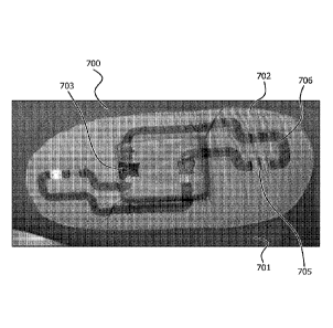
[0049] In another embodiment, depicted in FIG. 7, an electronic module
703
may be physically and electrically connected (coupled) to the conductive trace
positioned on the surface of the microporous synthetic polymer membrane 702
(e.g.,
flexible printed circuit or flexible printed circuit board) to form a hybrid
flexible printed
12
CA 03097113 2020-10-14
WO 2019/216883 PCT/US2018/031546
circuit board 700. An electronic module is defined herein as an assembly that
includes
more than two or more electronic components that are electrically coupled. An
insulative overcoat 706 may be positioned over all or portions of the
conductive trace. It
is to be appreciated that an imbibed conducive trace may alternatively be
used. In use,
the flexible printed circuit board 700 interfaces electrically with the
electronic module
703. Also, in at least one embodiment, the electronic module 703 may be
positioned
between the synthetic polymer membrane 702 and the skin 701. Such a
positioning of
the electronic module 703 creates a very durable device that is resistant to
damage
during use. Covering the electronic module with the synthetic polymer membrane
702
reduces or even minimizes the risk of catching the edge of the module and
peeling it off
as the user engages in activities or otherwise engages with the environment.
The
generally slippery nature of synthetic polymer membranes, especially expanded
polytetrafluoroethylene (ePTFE), creates a low friction interface between the
device and
the wearer's clothing, giving the wearer the ability to move freely with the
flexible printed
circuit board discretely located on a portion of the body that may be hidden
by clothing.
In some embodiments, an insulative overcoat 706 may be applied over the
electrically
conductive trace 705 to assist in protecting the electrically conductive trace
705 from
external elements, such as, but not limited to, abrasion and water. It is to
be noted that
an insulative overcoat may be applied over any conductive trace described
herein.
Non-limiting examples of materials used to form the insulative overcoat
include
urethanes, acrylics, silicones, Styrene Isoprene Butadiene Block Copolymers,
Viton TM
FKM (a synthetic rubber and fluoropolymer elastorner), polyolefins, or
fluoropolymers.
[0050] Although not depicted in any figure, it is to be appreciated
that some
conductive trace may be located on the surface of a porous synthetic polymer
membrane as a consequence of the imbibing process. In embodiments where the
conductive trace is applied via a liquid carrier (e.g. an electrically
conductive ink) heat
may be applied to the flexible printed circuit to remove the liquid carrier.
The
temperature applied may be sufficient to at least partially fuse the
conductive trace (e.g.,
metal particles) in the synthetic polymer membrane to form a continuous
network of
conductive particles. In other embodiments, such as where the conductive trace
is
applied to the surface of the microporous synthetic polymer membrane, heat may
be
13
CA 03097113 2020-10-14
WO 2019/216883 PCT/US2018/031546
applied to at least partially melt the conductive trace (e.g., metal
particles) to form a
continuous network of conductive particles on the surface of the synthetic
polymer
membrane. At least partial melting the conductive trace is one way to
establish
electrical conductance of the conductive trace. In further embodiments, heat
may be
used to remove ligands or other processing aids from the conductive particles.
[0051] Advantageously, the flexible printed circuits described herein
are highly
flexible, having a flexibility of less than about 1.0 newton as evidenced by
the Peak
Compression Load Test (Compressive Buckling) test method set forth below. In
some
embodiments, the flexibility is less than about 0.9 newtons, less than about
0.8
newtons, less than about 0.7 newtons, less than about 0.6 newtons, less than
about 0.5
newtons, less than about 0.4 newtons, less than about 0.3 newtons, less than
about 0.2
newtons, or less than about 0.1 newton. In addition, the flexible printed
circuits are
extremely durable, where the load applied to cause a 2X increase in resistance
is
greater than about 6.0 newtons when tested according to the Load Required to
Double
the Resistance Test set forth below. In some embodiments, the load is greater
than
about 0.7 newtons, greater than about 1.0 newtons, greater than about 1.4
newtons,
greater than about 2.0 newtons, greater than about 3.0 newtons, or greater
than about
5.0 newtons. The flexible circuit board is also comfortable, as evidenced by
the On Skin
Comfort Test below, which received scores in the most comfortable range.
[0052] The flexible printed circuits, the flexible printed circuit
board, and the
hybrid flexible printed circuit board reach a balance of comfort, flexibility,
and durablility.
For instance, materials such as PET and Kapton are not comfortable, but are
durable.
Also, soft and comfortable materials such as urethanes are not durable. Also,
stiff
materials such as Mylar (i.e., polyethylene terephthalate (PET)) or Kapton
are durable,
but not flexible.
TEST METHODS
[0053] It should be understood that although certain methods and
equipment
are described below, other methods or equipment determined suitable by one of
ordinary skill in the art may be alternatively utilized.
[0054] ATEQ Airflow
14
CA 03097113 2020-10-14
WO 2019/216883 PCT/US2018/031546
[0055] ATEQ Airflow is a test method for measuring laminar volumetric
flow
rates of air through membrane samples. For each membrane, a sample was clamped
between two plates in a manner that seals an area of 2.99 cm2 across the flow
pathway.
An ATEQ (ATEQ Corp., Livonia, MI) Premier D Compact Flow Tester was used to
measure airflow rate (L/hr) through each membrane sample by challenging it
with a
differential air pressure of 1.2 kPa (12 mbar) through the membrane.
[0056] Gurley Airflow
[0057] The Gurley air flow test measures the time in seconds for 100
cm3 of
air to flow through 1 in2 (- 6.45 cm2) sample at 0.177 psi (- 1.22 kPa) of
water pressure.
The samples were measured in a GURLEYTM Densometer and Smoothness Tester
Model 4340 (Gurley Precision Instruments, Troy, NY). The values reported are
an
average of 3 measurements and are in the units of seconds.
[0058] Non-Contact Thickness
[0059] Non-contact thickness was measured using a laser micrometer
(Keyence model no. LS- 7010, Mechelen, Belgium). As shown in FIGS. 17A and B,
a
metal cylinder 1701 was aligned between a laser micrometer source 1702 and a
laser
micrometer receiver 1703. The shadow 1705 of the top of the cylinder 1701 is
projected
onto receiver 1703 as shown in FIG 17A. The position of the shadow was then
reset as
the "zero" reading of the laser micrometer. As shown in FIG. 17B, a single
layer of
membrane 1204 is draped over the surface of the metal cylinder 1701 without
overlap
and without wrinkles, casting shadow 1706 onto the receiver 1703. The laser
micrometer then indicated the change in the position of the shadows 1705 and
1706 as
the thickness of the sample. Each thickness was measured three times and
averaged
for each sample.
[0060] Mass per Area (Mass/Area)
[0061] The mass per area of samples was measured according to the ASTM
D 3776 (Standard Test Methods for Mass Per Unit Area (Weight) of Fabric) test
method
(Option C) using a Mettler-Toledo Scale, Model 1060. The scale was
recalibrated prior
to weighing specimens, and the results were reported in grams per square meter
(g/m2).
CA 03097113 2020-10-14
WO 2019/216883 PCT/US2018/031546
[0062] Moisture Vapor Transmission Rate (MVTR) Measurement for Skin
Contact Samples
[0063] Approximately 70 m L of a solution consisting of 35 parts by
weight of
potassium acetate and 15 parts by weight of distilled water was placed into a
133-m L
polypropylene cup having an inside diameter of 6.5 cm at its mouth. An
expanded
polytetrafluoroethylene (ePTFE) membrane having a minimum MVTR of
approximately
85,000 g/m2/24 hr as tested by the method described in U.S. Patent No.
4,862,730 to
Crosby, was attached to the lip of the cup using a rubber band to create a
taut, leak-
proof, microporous barrier containing the solution, creating a cup assembly.
[0064] A similar expanded polytetrafluoroethylene (ePTFE) membrane
having
an MVTR of approximately 85,000 g/m2/24 hr as tested by the method described
in U.S.
Patent No. 4,862,730 to Crosby was mounted to the surface of a water bath. The
water
bath assembly was controlled at 23 0.2 C, utilizing a temperature
controlled room and
a water circulating bath.
[0065] A sheet of office paper was cut to 180 mm square with a 90 mm
diameter hole in the center. Release paper on an adhesive backed flexible
printed
circuit was removed while the substrate was supported in a hoop, and the
office paper
was applied to the adhesive so that the printed pattern was approximately
centered
within the 90 mm hole in the office paper. The flexible printed circuit was
then removed
from the hoop. The office paper support allowed the flexible printed circuit
to be more
easily handled during testing. Excess substrate was trimmed and discarded.
[0066] The adhesive-backed flexible printed circuit with a paper
boarder was
placed adhesive side up onto the expanded polytetrafluoroethylene membrane
mounted
to the surface of the water bath and allowed to equilibrate for at least 15
minutes prior to
the introduction of the cup assembly.
[0067] The expanded polytetrafluoroethylene end of the cup assembly
was
pressed against the adhesive, which was approximately centered within the hole
in the
support paper. The cup and sample were quickly removed from the water bath,
weighed to the nearest 1/1000 g, and placed back into the water bath.
[0068] Water transport was provided by the driving force between the
water in
the water bath and the saturated salt solution providing water flux by
diffusion in that
16
CA 03097113 2020-10-14
WO 2019/216883 PCT/US2018/031546
direction. The sample rested for 60 minutes and the cup assembly was then
removed,
weighed again within 1/1000 g.
[0069] The moisture vapor transmission rate (MVTR) of the sample was
calculated from the weight gain of the cup assembly and was expressed in grams
of
water per square meter of sample surface area per 24 hours.
[0070] Matrix Tensile Strength Determination
[0071] A synthetic polymer membrane was cut in each the longitudinal
and
transverse directions using an ASTM D412-Dogbone F. The "machine direction" is
in
the direction of the extrusion and the "transverse direction" is parallel to
this. The
membrane was placed on a cutting table such that the membrane was free from
wrinkles in the area in which the membrane was to be cut. A die was then
placed on
the membrane (generally in the center 200 mm of the membrane) such that its
long axis
was parallel to the direction that would be tested. Once the die was aligned,
pressure
was applied to cut through the synthetic polymer membrane. Upon removal of the
pressure, the dogbone sample was inspected to ensure it was free from edge
defects
which may impact the tensile testing. At least 3 dogbone samples in the
machine
direction and three dogbone samples in the transverse direction were prepared
in this
manner. Once the dogbone samples were prepared, they were measured to
determine
their mass using an analytical balance and their thickness using a Mitutoyo
547-400S
thickness gauge.
[0072] Tensile break load was measured using an INSTRON 5500R
(Illinois
Tool Works Inc., Norwood, MA) tensile test machine equipped with a rubber
coated face
plate and a serrated face plate such that each end of the dogbone sample was
held
between one rubber coated plate and one serrated plate. The pressure applied
to the
grip plates was approximately 552 kPa. The gauge length between the grips was
set at
58.9 mm and the crosshead speed (pulling speed) was set to a speed of 508
mm/min.
A 500 N load cell was used to carry out these measurements and data was
collected at
a rate of 50 points/sec. The laboratory temperature was between 20 C and 22.2
C to
ensure comparable results. If the dogbone sample broke at the grip interface,
the data
was discarded. At least three dogbone samples in the machine direction and
three
17
CA 03097113 2020-10-14
WO 2019/216883 PCT/US2018/031546
dogbone samples in the transverse direction were successfully pulled (i.e., no
slipping
out of or breaking at the grips) in order to characterize the dogbone samples.
[0073] The following equation was used to calculate the matrix tensile
strength:
MTS = ((Fmax/w)* p )/ mass:area, in which:
MTS = matrix tensile strength in MPa,
Fmax = maximum load measured during test (newtons),
w = width of dogbone sample within the gauge length (meters),
p = density of PTFE (2.2x10⁶ g/m3) or density of polyethylene (0.94 g/m3),
and
mass:area = mass per area of the sample (g/m2).
[0074] Bubble Point
[0075] Bubble point pressures were measured according to the general
teachings of ASTM F31 6-03 using Porometer (Model 3Gzh from Quantachrome
Instruments, Boynton Beach, Florida). The sample membrane was placed into the
sample chamber and wet with Silwick Silicone Fluid (available from Porous
Materials
Inc.) having a surface tension of 20.1 dynes/cm. The bottom clamp of the
sample
chamber had a 2.54 cm diameter, 0.159 cm thick porous metal disc insert
(Quantachrome part number 75461 stainless steel filter) and was used to
support the
sample. Using the 3GWin software version 2.1, the following parameters were
set as
specified in the table immediately below. The values presented for bubble
point
pressure are the average of two measurements. Bubble point pressure was
converted
to pore size using the following equation:
DBP = 4y1vcose / PBP
where DBP is the pore size, ylv is the liquid surface tension, e is the
contact
angle of the fluid on the material surface, and PBP is the bubble point
pressure. It is
understood by one skilled in the art that the fluid used in a bubble point
measurement
must wet the surface of the sample.
18
CA 03097113 2020-10-14
WO 2019/216883
PCT/US2018/031546
Bubble Point Instrument Settings
Parameter
0.
Run Settings
Starting pressure 2.12 psig
Ending pressure 85.74 psig
Sample Area 3.14 cm2
Run Type Wet Only
Number Data Points 256
Pressure Control
Use Normal Equilibrium TRUE
Use Tol FALSE
Use Time FALSE
Use Rate FALSE
Use Low Flow Sensor FALSE
Time Out NA
Equil Time NA
Run Rate NA
Pressure Tolerance NA
Flow Tolerance NA
Smoothing
UseMovAve FALSE
MovAveWet Interval NA
MovAveDry Interval NA
Lowess Dry 0.050
Lowess Wet 0.050
Lowess Flow 0.050
Lowess Num 0.100
MinSizeThreshold 0.98
Bubble Point Parameters
UseBpAuto TRUE
UseBpThreshold (L/min) FALSE
UseBpThreshold (Abs/cm2) FALSE
UseBpThresholdNumber FALSE
19
CA 03097113 2020-10-14
WO 2019/216883 PCT/US2018/031546
Parameter
BpAutoTolerance (manual) 1%
BpThresholdValue (manual) NA
BpThreshold (abs/cm2) 0
value
[0076] Load Required to Double the Resistance Test
[0077] A flexible printed circuit was placed in a mechanical property
testing
machine (INSTRON Model 5965, Illinois Tool Works Inc., Glenview, IL). The
flexible
printed circuit was stretched and the load (newtons) required to achieve a
doubling of
the resistance was measured.
[0078] An adhesive backed flexible printed circuit was trimmed so that
a
single printed conductive line 401 shown in FIG. 4 was centered within a 15 mm
wide
strip. The grips of the INSTRON Model 5965 were positioned 100 mm apart and
the
flexible printed circuit was gripped so that the printed feature (conductive
line) was
roughly centered within the gap. Matching source and sense leads of a KEITHLY
580
micro ohmmeter were each connected to the two ends of the printed line 401 and
the
load cell was zeroed. The flexible printed circuit was strained using a
crosshead speed
of 10 mm/minute. Resistance of the conductive trace and the load applied to
the
flexible printed circuit were captured concurrently. As the test progressed,
the
resistance of the conductive trace increased. The load applied to the flexible
printed
circuit when the resistance reached a value that was double the initial
resistance was
recorded and reported in newtons.
[0079] Peak Compression Load Test (Compressive Buckling)
[0080] Two 15 mm diameter aluminum cylinders 100, 110 as shown in FIG.
6
were fabricated and mounted in an INSTRON Model 5965 so that the cylinders
were
concentric, with one cylinder attached to the frame and the other attached to
the
crosshead. The free edges 104, 114 of the cylinders were positioned 10 mm
apart, and
the 100 N load cell on the crosshead was zeroed.
CA 03097113 2020-10-14
WO 2019/216883 PCT/US2018/031546
[0081] An adhesive backed flexible printed circuit 102 having thereon
a
release liner was prepared by removing the release paper and dusting the
adhesive
with powdered talc. The talc eliminated the tackiness of the adhesive without
significantly affecting the mechanical properties of the flexible printed
circuit, and made
the flexible printed circuit 102 easier to handle. The flexible printed
circuit 102 was then
cut to a size of 70 mm x 25 mm with the printed features 101 parallel to the
shorter side
and approximately centered with respect to the longer side. The flexible
printed circuit
102 was wrapped around the aluminum cylinders 100, 110, spanning the 10 mm gap
and overlapping each cylinder 100, 110 by approximately 7.5 mm as shown in
FIG. 6.
The flexible printed circuit 102 was attached to the cylinders 100, 110 using
19-mm
wide paper tape 103, 113 (89097-990, VWR Scientific (a division of Avantor),
Radnor,
PA) in a manner that minimized wrinkles in the flexible printed circuit 102.
One edge of
the tape 103 was aligned with the free edge 104 of the aluminum cylinder 100.
One
edge of the tape 113 was aligned with the free edge 114 of the other aluminum
cylinder
110. A 10 mm gap was maintained between the aluminum cylinders 100, 110 in
which
only the flexible printed circuit 102 was present.
[0082] Prior to testing, the aluminum cylinders 100, 110 were
positioned so
that a tensile load between 0.5 N and 1.5 N was applied to the flexible
printed circuit
102. The crosshead was then moved at a rate of 10 mm/mmn until the distance
between
the free edges 104, 114 of the aluminum cylinders 100, 110 was reduced to 5
mm. The
peak compressive load required to compress and buckle the flexible printed
circuit 102
was recorded. This test was performed on three different specimens from the
same
flexible printed circuit 102 and the average of these three tests was recorded
and
reported in Newtons.
[0083] On-Skin Comfort Test
[0084] An adhesive backed flexible printed circuit with a release
liner was
trimmed to a rectangular shape that was 90 mm long and 25 mm wide. A 25 mm
wide
strip of polyester tape 8992 (3M, St Paul, MN) was applied to the printed side
of the
flexible printed circuit to act as a transfer tape during application. The
skin within and
around the cubital fossa (interior bend of elbow) of a volunteer was prepared
by wiping
the skin with an alcohol prep pad and allowing the skin to dry. The paper
release liner
21
CA 03097113 2020-10-14
WO 2019/216883 PCT/US2018/031546
was removed from the flexible printed circuit 710 and the exposed adhesive
(not
illustrated) was applied to the volunteer's arm so that it crossed the cubital
fossa 720
and was approximately oriented as depicted in FIG. 5. The polyester tape was
carefully
removed, leaving the flexible printed circuit 710 (i.e., synthetic polymer
membrane with
conductive traces thereon) adhered to the skin. One inventive flexible printed
circuit
710 was applied to one arm and a comparative printed circuit (not illustrated)
made in
accordance with Example 7 was applied to the other arm of each volunteer. The
volunteer was asked to wear the flexible printed circuits for up to 8 hours,
and to rank
the comfort on a scale of 1 to 10, where 1 was the least comfortable, and 10
was the
most comfortable. The ranking guidelines proposed to each volunteer were as
follows:
Most comfortable. Could barely feel it, easy to forgot about it
9
Comfortable 8 Occasionally noticed it during extreme activities or
motions
Range 7
6 Occasionally noticed it during routine activities.
Don't mind
wearing it
5 Occasionally noticed it during routine activities.
Would
prefer not to wear it.
Uncomfortable 4
Range 3 Regularly noticed it, irritating, eager to remove it
2
1 Least comfortable. Noticed it constantly; caused
significant
irritation; very eager to remove it, or removed it early
[0085] The results reported are an average of at least 4 tests.
ePTFE MEMBRANES
[0086] ePTFE Membrane 1 - Preparation ePTFE Membrane
[0087] An ePTFE membrane was manufactured according to the general
teachings set forth in U.S. Patent Publication No. 2004/0173978 to Bowen etal.
The
22
CA 03097113 2020-10-14
WO 2019/216883 PCT/US2018/031546
ePTFE membrane had a mass-per-area of 4.6 g/m2, a porosity of 87%, a non-
contact
thickness of 15.5 pm, a Gurley number of 4.5 seconds, an ATEQ air flow of 17
liters/cm2/hour at 12 mbar, a matrix tensile strength of 258 MPa in the
machine
direction, a matrix tensile strength of 329 MPa in the transverse direction, a
specific
surface area of 14.520 m2/g, and a surface area per volume of 31.944 m2/cm3. A
scanning electron microscope (SEM) image of the ePTFE membrane is shown in
FIG.
1.
[0088] ePTFE Membrane 2 - Preparation ePTFE Membrane
[0089] An ePTFE membrane was manufactured according to the general
teachings set forth in U.S. Patent No. 3,953,566 to Gore. The ePTFE membrane
had a
mass-per-area of 16.6 g/m2, a porosity of 80%, a non-contact thickness of 37.6
pm, a
bubble point of 156 kPa, a matrix tensile strength of 42.4 MPa in the machine
direction,
a matrix tensile strength of 116.4 MPa in the transverse direction, a specific
surface
area of 7.891 m2/g and a surface area per volume of 17.75 m2/cm3. An SEM image
of
the ePTFE membrane is shown in FIG. 2.
EXAMPLES
[0090] The invention of this application has been described above both
generically and with regard to specific embodiments. It will be apparent to
those skilled
in the art that various modifications and variations can be made in the
embodiments
without departing from the scope of the disclosure. Thus, it is intended that
the
embodiments cover the modifications and variations of this invention provided
they
come within the scope of the appended claims and their equivalents.
EXAMPLE 1
[0091] A flexible printed circuit was manufactured and combined with a
dermally acceptable adhesive. Expanded polytetrafluoroethylene (ePTFE)
membrane
(Membrane 1) was used as substrate for printing.
[0092] To prepare the ePTFE for imbibing, the ePTFE membrane was
restrained by laying it over a 6-inch diameter aluminum hoop, fixing it to the
hoop by
23
CA 03097113 2020-10-14
WO 2019/216883 PCT/US2018/031546
placing a stainless steel spring around the circumference, and tensioning the
substrate
to remove wrinkles. To support the ePTFE membrane during adhesion of a
stencil, the
hoop restraining the ePTFE membrane was placed over a clean DELRIN (an acetal
homopolymer resin available from DowDuPont, Wilmington, DE) disc that was
machined to fit inside the hoop, and which provided a clean surface that
contacted the
"bottom" of the ePTFE membrane.
[0093] To prepare the stencil, a piece of tape (Scapa Type 536; a
polyester
film, single coated with an acrylic adhesive; Scapa North America, Windsor,
CT) was
transferred to the release paper, and a laser cutter (PLS6.75 laser cutter,
Universal
Laser, Scottsdale, AZ) was used to cut holes in the tape stencil in the
pattern shown in
FIG 4. The dimensions shown in FIG. 4 are in mm and are shown for to indicate
the
size of the pattern. The double ended arrow 402 is shown to illustrate the
alignment of
the ePTFE membrane with the conductive trace.
[0094] The tape stencil was then removed from the release paper and
pressed by hand to the surface of the exposed "top" surface of the ePTFE
membrane to
firmly adhere the stencil to the ePTFE membrane. The tape stencil was oriented
on the
ePTFE membrane so that the arrow 402 in FIG. 4 was aligned with the transverse
direction of the ePTFE membrane. The stencil and ePTFE membrane, still
restrained
on the hoop, were then removed from the DELRIN disc and placed in a
laboratory
fume hood for imbibing. An excess of conductive ink (2108-IPA available from
Nanogap, Inc.) was pipetted onto the top surface of the ePTFE membrane through
the
holes in the tape stencil. When this process was complete, the top surface of
the
stencil/ ePTFE membrane was thoroughly wiped with a cellulose fiber wiper
(KIMWIPES ; Kimberly Clark, Delicate Task Wiper, 1-ply) to remove any excess
ink.
The tape stencil was then promptly removed. Removal of the stencil also
removed a
portion of the upper surface of the ePTFE membrane that was adhered to the
stencil,
but the amount was considered negligible. The imbibed ePTFE membrane (flexible
printed circuit), still restrained in the hoop, was then allowed to air dry in
the hood for at
least 10 minutes, and then heat-treated in a hot air convection oven for 60
minutes at
200 C.
[0095] Dermal adhesive and lamination
24
CA 03097113 2020-10-14
WO 2019/216883 PCT/US2018/031546
[0096] A dermally acceptable adhesive, ARCARE 7396 (a pressure-
sensitive
tape with MA-38 medical grade acrylic adhesive; Adhesives Research, Glen Rock,
PA)
was selected. The adhesive was provided on a roll supported by paper release
liner.
The release liner with adhesive was cut into a square at least 130 mm x 130 mm
and
applied by hand to the side of the ePTFE membrane opposing the side on which
the
conductive ink was applied. The printed pattern was approximately centered
relative to
the adhesive. With the eTPFE membrane supported by a lab bench, pressure was
applied by hand to the release paper, pressing the adhesive firmly to the
printed flexible
circuit.
[0097] Load Required to Double the Resistance Test
[0098] The flexible printed circuit was tested using the Load Required
to
Double the Resistance Test described in the Test Method section set forth
above. The
load applied to cause a 2X increase in resistance was determined to be 1.49
Newtons
(Table 1).
[0099] MTVR
[0100] The moisture vapor transmission rate was measured as described
in
the test method entitled "Moisture Vapor Transmission Rate (MVTR) Measurement
for
Skin Contact Samples" set forth above. The MVTR was determined to be 593
g/m2/24
hours (Table 1).
[0101] Peak Compression Load Test
[0102] The peak load measured was measured as described in the test
method entitled "Peak Compression Load Test (Compressive Buckling)". The peak
load
was determined to be 0.0471 Newtons (Table 1).
EXAMPLE 2
[0103] A flexible printed circuit was manufactured and combined with a
dermally acceptable adhesive. Expanded polytetrafluoroethylene membrane
(Membrane 1) was used as substrate for printing.
[0104] Surface-printing conductive traces onto a substrate for skin
contact
CA 03097113 2020-10-14
WO 2019/216883 PCT/US2018/031546
[0105] The ePTFE membrane was restrained in a 356 mm diameter
embroidery hoop, tensioned to remove wrinkles, and screen-printed using
conductive
ink in the pattern shown in FIG 4. The dimensions shown in FIG. 4 are in mm
and are
shown to indicate the size and shape of the pattern. The double ended arrow
402 is
shown to illustrate the alignment of the ePTFE membrane with the conductive
trace.
The conductive ink used was CI1036 (Engineered Conductive Materials, Delaware,
OH). The ink was thinned with 8.7% methyl ethyl ketone (MEK) by weight prior
to
printing. The screen printing was performed using a model MSP-088 screen
printer
(HMI Manufacturing, Lebanon, NJ), a stainless steel screen with 200 TPI
(threads/wire
per inch; -78,74 wires per cm), 1.6 mil (- 40.64 pm) wire diameter, and a 12.7
micron
emulsion of the ink. The printing was performed so that the arrow 402 in FIG.
4 was
aligned with the transverse direction of the ePTFE membrane. After printing
the ink was
then dried in a convection oven at 120 C for 20 minutes.
[0106] Dermal adhesive and lamination
[0107] Dermal adhesive and lamination was conducted according the
process
described in Example 1.
[0108] Load Required to Double the Resistance Test
[0109] The flexible printed circuit was tested using the Load Required
to
Double the Resistance Test described in the Test Method section set forth
above. The
load applied to cause a 2X increase in resistance was determined to be 2.3788
Newtons (Table 1).
[0110] MTVR
[0111] The moisture vapor transmission rate was measured using the
test
method entitled "Moisture Vapor Transmission Rate (MVTR) Measurement for Skin
Contact Samples" set forth herein. The MVTR was determined to be 586 g/m2/24
hours
(Table 1).
[0112] Peak Compression Load Test
[0113] The peak load was measured as described in the test method
entitled
"Peak Compression Load Test (Compressive Buckling)" set forth above. The peak
load
was determined to be 0.0815 Newtons (Table 1).
26
CA 03097113 2020-10-14
WO 2019/216883 PCT/US2018/031546
EXAMPLE 3
[0114] A flexible printed circuit was manufactured and combined with a
dermally acceptable adhesive. Expanded polytetrafluoroethylene (ePTFE)
membrane
(ePTFE Membrane 2) was used as the substrate for printing.
[0115] Surface-printing conductive traces onto a substrate for skin
contact
[0116] Surface printing of the conductive trace on the ePTFE substrate
was
conducted using the procedure described in Example 2.
[0117] Dermal adhesive and lamination
[0118] Dermal adhesive and lamination was conducted according the
process
described in Example 1.
[0119] Load Required to Double the Resistance Test
[0120] The flexible printed circuit was tested using the Load Required
to
Double the Resistance Test described in the Test Method section set forth
above. The
load applied to cause a 2X increase in resistance was determined to be 1.5183
Newtons (Table 1).
[0121] MTVR
[0122] The moisture vapor transmission rate was measured using the
test
method entitled "Moisture Vapor Transmission Rate (MVTR) Measurement for Skin
Contact Samples" set forth herein. The MVTR was determined to be 745 g/m2/24
hours
(Table 1).
[0123] Peak Compression Load Test
[0124] The peak load was measured as described in the test method
entitled
"Peak Compression Load Test (Compressive Buckling)" set forth above. The peak
load
was determined to be 0.1432 Newtons (Table 1).
[0125] On-Skin Comfort Test
[0126] On-skin comfort was determined utilizing the test method
entitled "On-
Skin Comfort Test" set forth above. The average rank score for the printed
circuit was
determined to be 8.5 (Table 1).
EXAMPLE 4
27
CA 03097113 2020-10-14
WO 2019/216883 PCT/US2018/031546
[0127] A flexible circuit was manufactured and combined with a
dermally
acceptable adhesive. A porous polyethylene lithium ion battery insulation
membrane,
(Pair Materials Co. Ltd, Dongguan, China) was obtained and used as the
printing
substrate. The polyethylene membrane had a mass-per-area of 7.0 g/m2, a
porosity of
40%, a thickness of 12.4 pm, a bubble point of 1543 kPa, a matrix tensile
strength of
314 MPa in the machine direction, a matrix tensile strength of233 MPa in the
transverse
direction, a gravimetric specific surface area of 34.1 m2/g, and a volumetric
specific
surface area of 32.1 m2/cm3. An SEM image of the membrane is shown in FIG. 3.
[0128] Surface-printing conductive traces onto a substrate for skin
contact
[0129] Surface printing of the conductive trace on the polyethylene
(PE)
substrate was conducted using the procedure described in Example 2.
[0130] Dermal adhesive and lamination
[0131] Dermal adhesive and lamination was conducted according the
process
described in Example 1.
[0132] Load Required to Double the Resistance Test
[0133] The flexible printed circuit was tested using the Load Required
to
Double the Resistance Test described in the Test Method section set forth
above. The
load applied to cause a 2X increase in resistance was determined to be 5.6267
Newtons (Table 1).
[0134] MTVR
[0135] The moisture vapor transmission rate was measured using the
test
method entitled "Moisture Vapor Transmission Rate (MVTR) Measurement for Skin
Contact Samples" set forth herein. The MVTR was determined to be 340 g/m2/24
hours
(Table 1).
[0136] Peak Compression Load Test
[0137] The peak load was measured as described in the test method
entitled
"Peak Compression Load Test (Compressive Buckling)" set forth above. The peak
load
was determined to be 0.5826 Newtons (Table 1).
[0138] On-Skin Comfort Test
28
CA 03097113 2020-10-14
WO 2019/216883 PCT/US2018/031546
[0139] On-skin comfort was determined utilizing the test method
entitled "On-
Skin Comfort Test" set forth above. The average rank score for the flexible
printed
circuit was determined to be 9.8 (Table 1).
EXAMPLE 5
[0140] A flexible printed circuit was manufactured and combined with a
dermally acceptable adhesive. A 25 micron thick non-porous urethane film
(PT1710S,
Deerfield Urethanes, VVhately, Mass.) was obtained and used as the printing
substrate.
[0141] Surface-printing conductive traces onto a substrate for skin
contact
[0142] Surface printing of the conductive trace on the non-porous
urethane
substrate was conducted using the procedure described in Example 2.
[0143] Load Required to Double the Resistance Test
[0144] The flexible printed circuit was tested using the Load Required
to
Double the Resistance Test described in the Test Method section set forth
above. The
load applied to cause a 2X increase in resistance was determined to be 0.6875
Newtons (Table 1).
[0145] MTVR
[0146] The moisture vapor transmission rate was measured using the
test
method entitled "Moisture Vapor Transmission Rate (MVTR) Measurement for Skin
Contact Samples" set forth herein. The MVTR was determined to be 875 g/m2/24
hours
(Table 1).
[0147] Peak Compression Load Test
[0148] The peak load was measured as described in the test method
entitled
"Peak Compression Load Test (Compressive Buckling)" set forth above. The peak
load
was determined to be 0.04337 Newtons (Table 1).
EXAMPLE 6
[0149] A flexible printed circuit was manufactured and combined with a
dermally acceptable adhesive. An approximately 50.8 pm thick, clear
polyethylene
29
CA 03097113 2020-10-14
WO 2019/216883 PCT/US2018/031546
terephthalate (PET) film (Dura-Lar, McMaster-Carr 8567K22) was obtained and
used as
the printing substrate.
[0150] Surface-printing conductive traces onto a substrate for skin
contact
[0151] Surface printing of the conductive trace on the PET film
substrate was
conducted using the procedure described in Example 2.
[0152] Load Required to Double the Resistance Test
[0153] The flexible printed circuit was tested using the Load Required
to
Double the Resistance Test described in the Test Method section set forth
above. The
load applied to cause a 2X increase in resistance was determined to be 82.65
Newtons
(Table 1).
[0154] MTVR
[0155] The moisture vapor transmission rate was measured using the
test
method entitled "Moisture Vapor Transmission Rate (MVTR) Measurement for Skin
Contact Samples" set forth herein. The MVTR was determined to be 130 g/m2/24
hours
(Table 1).
[0156] Peak Compression Load Test
[0157] The peak load was measured as described in the test method
entitled
"Peak Compression Load Test (Compressive Buckling)" set forth above. The peak
load
was determined to be 19.7540 Newtons (Table 1).
EXAMPLE 7
[0158] A flexible printed circuit was manufactured and combined with a
dermally acceptable adhesive. An approximately 12.7 pm thick, clear
polyethylene
terephthalate (PET) film (Dura-Lar, McMaster-Carr 8567K104) was obtained and
used
as the printing substrate.
[0159] Surface-printing conductive traces onto a substrate for skin
contact
[0160] Surface printing of the conductive trace on the PET film
substrate was
conducted using the procedure described in Example 2.
[0161] Load Required to Double the Resistance Test
CA 03097113 2020-10-14
WO 2019/216883 PCT/US2018/031546
[0162] The flexible printed circuit was tested using the Load Required
to
Double the Resistance Test described in the Test Method section set forth
above. The
load applied to cause a 2X increase in resistance was determined to be 20.9
Newtons
(Table 1).
[0163] MTVR
[0164] The moisture vapor transmission rate was measured using the
test
method entitled "Moisture Vapor Transmission Rate (MVTR) Measurement for Skin
Contact Samples" set forth herein. The MVTR was determined to be 80 g/m2/24
hours
(Table 1).
[0165] Peak Compression Load Test
[0166] The peak load was measured as described in the test method
entitled
"Peak Compression Load Test (Compressive Buckling)" set forth above. The peak
load
was determined to be 0.9335 Newtons (Table 1).
[0167] On-Skin Comfort Test
[0168] On-skin comfort was determined utilizing the test method
entitled "On-
Skin Comfort Test" set forth above. The average rank score for the sample was
determined to be 4.3 (Table 1).
EXAMPLE 8
[0169] An ePTFE membrane made generally according to the teachings
described in U.S. Patent No. 3,953,566 to Gore was provided. The ePTFE
membrane
had a mass per area of about 19 g/m2, a porosity of about 56%, a thickness of
about 25
pm, a bubble point of about 159 KPa, a matrix tensile strength of about 48 MPa
in the
longitudinal direction, and a matrix tensile strength of about 97 MPa in the
transverse
direction.
[0170] The ePTFE membrane was restrained in a 14 inch (-35.56 cm)
diameter embroidery hoop and screen printed using conductive ink (CI1036;
Engineered
Conductive Materials, Delaware, OH) in the pattern shown in FIG. 8. The
dimensions
shown in FIG. 8 are in mm and are shown for to indicate the size and print of
the
pattern. The screen printing was performed using a model MSP-088 screen
printer
(HMI Manufacturing, Lebanon, NJ), a stainless steel screen with 200 TPI, 1.6
mil wire
31
CA 03097113 2020-10-14
WO 2019/216883 PCT/US2018/031546
diameter, and 12.7 pm emulsion of the electrically conducive ink. The ink was
dried in a
convection oven at 160 C for 10 minutes. The electrically conductive trace on
the
ePTFE membrane is the flexible printed circuit.
[0171] A dielectric overcoat 910 (ink, stretchable, ultraviolet light
(UV)-cure
insulator; DI-7540; Engineered Conductive Materials, Delaware, OH) was then
applied
over most of the previously printed conductive trace 810 in the pattern shown
in FIG 9.
The dimensions shown in FIG. 9 are in mm and are shown to indicate the size
and print
of the pattern. The dielectric overcoat 910 was cured by exposing it to UV
light for
about 30 seconds using a PORTA-RAY 400 (a portable UV light curing system;
Dymax
Corp., Torrington, CT).
[0172] A surface mount light-emitting diode (LED) 331 was adhered to
the
printed ePTFE membrane 360 using electrically conductive ink (C 11036
Engineered
Conductive Materials, Delaware, OH) as shown in FIG. 10 to create a flexible
printed
circuit board. Additional ink was applied to make an electrical connection 332
as shown
in FIG. 10. The conductive ink was dried in a convection oven at 130 C for
approximately 10 minutes. A UV-curable encapsulant (EC-9519; Engineered
Conductive Materials, Delaware, OH) was applied over the LED 331 and
electrical
connection 332. The encapsulant was cured with 30 seconds of UV exposure in a
400
watt Dymax cure station (Dymax Corp.).
[0173] ARCARE 7396 pressure sensitive adhesive (Adhesives Research,
Glen Rock, PA) was then applied to the unprinted side of the ePTFE membrane. H-
shaped cuts 337 were made in the ePTFE membrane 360 as shown in FIG. 10. The
resulting flaps 333, 334, 335, and 336, each supported an exposed trace of
conductive
ink, were folded to the back of the ePTFE membrane 360. A 3 mm circle of
ARCARE
90366 conductive pressure sensitive adhesive (Adhesives Research, Glen Rock,
PA)
was applied to each flap 333, 334, 335, and 336.
[0174] Next, an electronic module was prepared. An electronic module
is
defined herein as an assembly that includes more than two or more electronic
components that are electrically coupled. A single-sided1/16 inch thick copper
clad FR4
PCB 341 (473-1000-ND, Digi-Key, Thief River Rails, MN) was machined in the
outline
and copper pattern 342 shown in FIG. 11. A battery 343 (3V lithium battery;
coin shape,
32
CA 03097113 2020-10-14
WO 2019/216883 PCT/US2018/031546
12.5 mm; P663-ND, Digi-Key, Thief River Falls, MN), a processor 344 (Atmel 8-
bit AVR
Microcontroller; ATTINY85V-10SU-ND, Digi-Key, Thief River Falls, MN), and a 1
pF
capacitor 345 (445-8890-1-ND, Digi-Key, Thief River Falls, MN) were soldered
to the
copper traces as shown in FIG. 11. Header pins were placed in through-holes in
the
board at locations 346, 347, 348, 349 so that the pins were nearly flush with
the copper
traces and protruded several mm through the board. A two-part housing 500
having a
first half 510 and a second half 520 was machined from polycarbonate with a
wall
thickness of about 0.3 mm and outside dimensions of about 25.2 mm x 19.4 mm x
4
mm and is shown in FIG. 12. The flexible printed circuit board was glued into
one half of
the housing using epoxy adhesive (Locktite 79340-68620, Henkel Corp. Rocky
Hill, CT)
with the header pins extending through the housing.
[0175] Once the epoxy cured, the header pins were clipped and ground
flush
with the housing, creating electrical contacts. ECOFLEXTM 00-35 FAST Silicone
(a soft,
fast cure platinum-catalyzed silicone; Smooth-on, Macungie, PA) was poured
into the
housing and allowed to surround the circuit board. The second half 520 of the
housing
was assembled onto the first half 510 and held in place while the silicone
cured.
Electrically conductive ink (CI1036, Engineered Conductive Materials,
Delaware, OH)
was printed onto the housing and on top of the electrical contacts 365, 366,
367, 368
forming features 361, 362, 363, and 364 in the pattern shown in FIG. 13. The
conductive ink was allowed to dry in an oven for 20 minutes at 60 C.
[0176] The electronic module 300 was attached to the flexible circuit
350 so
that the flaps 333, 335, 334, and 336 in FIG. 10 were connected to the
conductive ink
portions 364, 362, 362, and 361 shown in FIG. 13, respectively. This created a
hybrid
flexible printed circuit board that included an electronic module and the
flexible printed
circuit board. The processor 334 in FIG. 11 was pre-programmed to flash the
LED 331
times after the electrical contacts 338 were connected with an electrically
conductive
object. This demonstrated that the electronic module was able to communicate
electrically with the hybrid flexible printed circuit board.
[0177] The hybrid flexible printed circuit board was removed from the
embroidery hoop by trimming the ePTFE membrane around the perimeter of the
conductive ink, leaving an approximately 5-10 mm border. The hybrid flexible
printed
33
CA 03097113 2020-10-14
WO 2019/216883 PCT/US2018/031546
circuit board was attached to the forearm of a subject while the subject's arm
was
straight at the elbow and the subject's wrist was in full extension, as
pictured in FIG. 15.
Holding this position while attaching the hybrid flexible printed circuit
board kept the
subject's skin in tension. When the subject relaxed his elbow and wrist, the
flexible
circuit board easily conformed to the skin by compressing and wrinkling, as
shown in
FIG. 16. It was noted that after 5 days of wear, the hybrid flexible printed
circuit board
continued to function.
34
Table 1 - Summary of Data
o
Example Printing Conductive Ink Load
@ 2X Moisture Vapor Compressive On-Skin t..)
o
,-,
,o
Substrate Location Resistance
Transmission Buckling Comfort test
,-,
o,
(Newton) Rate
Average Peak Scale 00
00
(...)
(g/m2/24 hours)
Load (1-10)b
(newton)
1 ePTFE Type I Imbibed 1.490 593
0.05 N.D.a
2 ePTFE Type I Surface 2.379 586
0.08 N.D.
3 ePTFE Type 2 Surface 1.518
745 0.14 8.5
P
4 PE membrane Surface 5.627 340
0.58 9.8 c,
0
Urethane Surface 0.688 875 0.04
N.D. ,
,
(...)
,
(nonporous)
" c,
"
0
,
6 PET Surface 82.665 130
19.75 N.D. ,
0
,
,
50.8 pm
thickness
7 PET Surface 20.900 80
0.93 4.3
12.7 pm
thickness
od
n
a = Not determined (N.D.)
b = Scale from 1 (uncomfortable; most noticeable) to 10 (most comfortable;
least noticeable) cp
w
o
1¨
oe
O-
(...)
1¨
vi
.6.
o,