Note: Descriptions are shown in the official language in which they were submitted.
CA 03097955 2020-10-21
WO 2019/212453
PCT/US2018/030083
CONTROL METHOD FOR POWER CONVERTERS WITH INVERTER BLOCKS
WITH SILICON CARBIDE MOSFETS
FIELD
[0001] The present subject matter relates generally to power systems, and
more
particularly to systems and methods for providing gating commands to power
converters utilizing inverter blocks with silicon carbide MOSFETs.
BACKGROUND
[0002] Power generation systems can use power converters to convert power
into
a form of power suitable for an energy grid. In a typical power converter, a
plurality
of switching devices, such as insulated-gate bipolar transistors ("IGBTs") or
metal-
oxide-semiconductor field effect transistors ("MOSFETs") can be used in
electronic
circuits, such as half bridge or full-bridge circuits, to convert the power.
Recent
developments in switching device technology have allowed for the use of
silicon
carbide ("SiC") MOSFETs in power converters. Using SiC MOSFETs allows for
operation of a power converter at a much higher switching frequency compared
to
conventional IGBTs.
BRIEF DESCRIPTION
[0003] Aspects and advantages of embodiments of the present disclosure will
be
set forth in part in the following description, or may be learned from the
description,
or may be learned through practice of the embodiments.
[0004] One example aspect of the present disclosure is directed to a
control
method for operating a converter. The converter can include a plurality of
inverter
blocks. Each inverter block can include a plurality of switching devices. The
plurality of switching devices can include one or more silicon carbide
MOSFETs.
The control method can include providing, by a control system, one or more
gating
commands to a first inverter block in the plurality of inverter blocks. The
control
method can further include implementing, by the control system, a gating
command
delay to generate a first delayed gating command based at least in part on the
one or
more gating commands. The control method can further include providing, by the
1
CA 03097955 2020-10-21
WO 2019/212453
PCT/US2018/030083
control system, the first delayed gating command to a second inverter block in
the
plurality of inverter blocks.
[0005] Another example aspect of the present disclosure is directed to a
power
conversion system. The power conversion system can include a converter. The
converter can include a plurality of inverter blocks. Each inverter block can
include a
plurality of switching devices. The plurality of switching devices can include
one or
more silicon carbide MOSFETs. The power conversion system can also include a
control system comprising a plurality of gate drive cards. The control system
can be
configured to control operation of the converter by providing one or more
gating
commands to the plurality of inverter blocks. Each inverter block can have one
or
more associated gate drive cards from the plurality of gate drive cards
configured to
provide the one or more gating commands to the plurality of switching devices
in the
inverter block. At least one of the one or more associated gate drive cards
for each
inverter block can be daisy chained to at least one of the one or more
associated gate
drive cards of another inverter block.
[0006] Another example aspect of the present disclosure is directed a wind
power
generation system. The wind power generation system can include a wind power
generator configured to generate AC power and an AC to DC converter coupled to
the
wind power generator. The AC to DC converter can be configured to convert the
AC
power from the wind power generator to a DC power. The wind power generation
system can further include a DC link coupled to the AC to DC converter. The DC
link can be configured to receive DC power from the AC to DC converter. The
wind
power generation system can further include a DC to AC converter coupled to
the DC
link. The DC to AC converter can be configured to receive DC power from the DC
link. The DC to AC converter can include a plurality of inverter blocks. Each
inverter block can include a plurality of switching devices. The plurality of
switching
devices can include one or more silicon carbide MOSFETs. The wind power
generation system can further include a control system comprising a plurality
of gate
drive cards. The control system can be configured to control operation of the
DC to
AC converter by providing one or more gating commands to the plurality of
inverter
blocks. Each inverter block can have one or more associated gate drive cards
from
the plurality of gate drive cards configured to provide the one or more gating
2
CA 03097955 2020-10-21
WO 2019/212453
PCT/US2018/030083
commands to the plurality of switching devices in the inverter block. At least
one of
the one or more associated gate drive cards for each inverter block can be
daisy
chained to at least one of the one or more associated gate drive cards of
another
inverter block. The control system can be further configured to implement a
gating
command delay in gating commands provided by the gate drive cards.
[0007] Variations and modifications can be made to these example aspects of
the
present disclosure.
[0008] These and other features, aspects and advantages of various
embodiments
will become better understood with reference to the following description and
appended claims. The accompanying drawings, which are incorporated in and
constitute a part of this specification, illustrate embodiments of the present
disclosure
and, together with the description, serve to explain the related principles.
BRIEF DESCRIPTION OF THE DRAWINGS
[0009] Detailed discussion of embodiments directed to one of ordinary skill
in the
art are set forth in the specification, which makes reference to the appended
figures, in
which:
[0010] FIG. 1 depicts an example wind power generation system;
[0011] FIG. 2 depicts example elements for use in a power converter
according to
example aspects of the present disclosure;
[0012] FIG. 3 depicts a power converter according to example aspects of the
present disclosure;
[0013] FIG. 4 depicts a portion of a power converter according to example
aspects
of the present disclosure;
[0014] FIG. 5 depicts a control system for a power converter according to
example aspects of the present disclosure;
[0015] FIG. 6 depicts a graph of electromagnetic interference in
conventional
power converters;
[0016] FIG. 7 depicts a graph of electromagnetic interference in a power
converter according to example aspects of the present disclosure;
[0017] FIG. 8 depicts an example switching strategy according to example
aspects
of the present disclosure;
3
CA 03097955 2020-10-21
WO 2019/212453
PCT/US2018/030083
[0018] FIG. 9 depicts an example method according to example aspects of the
present disclosure; and
[0019] FIG. 10 depicts elements suitable for use in a control device
according to
example aspects of the present disclosure
DETAILED DESCRIPTION
[0020] Reference now will be made in detail to embodiments of the
invention,
one or more examples of which are illustrated in the drawings. Each example is
provided by way of explanation of the invention, not limitation of the
invention. In
fact, it will be apparent to those skilled in the art that various
modifications and
variations can be made in the present invention without departing from the
scope or
spirit of the invention. For instance, features illustrated or described as
part of one
embodiment can be used with another embodiment to yield a still further
embodiment. Thus, it is intended that the present invention covers such
modifications
and variations as come within the scope of the appended claims and their
equivalents.
[0021] As used herein, the terms "first," "second," and "third" may be used
interchangeably to distinguish one component from another and are not intended
to
signify location or importance of the individual components or limit the
number of
individual components in an apparatus. As used herein, the term
"approximately"
means within plus or minus ten percent of the stated value.
[0022] Example aspects of the present disclosure are directed to systems
and
methods for controlling a power converter with a plurality of inverter blocks
utilizing
SiC MOSFETs. For example, power generation systems, such as systems using
doubly fed induction generators ("DFIGs") as power generation units, can use
one or
more power converters to convert power from a low voltage multiphase
alternating
current power into a medium voltage multiphase alternating current power. As
used
herein, "LV" voltage can be a power less than about 1.5 kilovolts. As used
herein,
"MV" voltage can be power greater than about 1.5 kilovolts and less than about
100
kilovolts. As used herein, the term "about" can mean within 20% of the stated
value.
[0023] In an embodiment, the power converter can be a multiphase (e.g.,
three
phase) power converter configured to convert a multiphase power output from a
power generator. The power converter can include, for example, a first power
4
CA 03097955 2020-10-21
WO 2019/212453
PCT/US2018/030083
converter configured to convert an AC power output from a power generator,
such as
a DFIG, into a DC power, and provide the DC power to a DC link. A second power
converter can be configured to convert the DC power from the DC link into an
AC
power suitable for use on an energy grid. For example, the second power
converter
can be a DC to DC to AC power converter, and can utilize SiC MOSFETs as the
power semiconductors, thereby allowing very high switching frequency.
[0024] The second power converter can include, for example, a plurality of
inverter blocks. Each inverter block can include a plurality of bridge
circuits
configured to convert power, and each bridge circuit can include one or more
SiC
MOSFETs as switching devices. For example, each inverter block can be a DC to
DC
to AC inverter block, and a plurality of inverter blocks can be coupled in
parallel on a
LV side and coupled in series on a MV side. Each DC to DC to AC inverter block
can include a first DC to AC conversion entity configured to convert LV DC
power
from the DC link to a high frequency LV AC voltage, an isolation transformer
configured to provide isolation, a second AC to DC conversion entity
configured to
convert the LV AC power to a LV DC power, and a third DC to AC conversion
entity
configured to convert the LV DC power to an LV AC power suitable for use on an
energy grid. A plurality of inverter blocks can be connected in series to
build a MV
AC voltage suitable for use on a MV AC grid.
[0025] In an example topology, a plurality of inverter blocks can be
configured in
a three level topology from line to neutral, allowing an output voltage of a
positive
voltage, zero voltage, or a negative voltage for each phase. For example, the
power
converter can include six inverter blocks, with each inverter block including
a
plurality of switching devices, such as one or more SiC MOSFETs. A control
device
can provide one or more gating commands to each inverter block in order to
turn the
switching devices on and off to generate an output voltage waveform. For
example,
the control device can provide one or more gating commands to a plurality of
gate
drive cards, which can then turn the individual switching devices in an
inverter block
on and off
[0026] In such a system, each gate drive card may only be configured to
drive a
subset of the switching devices in an inverter block, such as, for example,
four
switching devices in a conversion entity forming a bridge circuit. Thus, for a
power
CA 03097955 2020-10-21
WO 2019/212453
PCT/US2018/030083
converter utilizing DC to DC to AC inverter blocks with three conversion
entities, at
least three gate drive cards may be required for each inverter block. Further,
in a
three phase power converter with six inverter blocks per phase, at least 54
gate drive
cards may be required to drive all of the switching devices in the power
converter.
However, a typical control device configured to provide gating commands to the
gate
drive cards may only have enough communication channels to provide gating
commands to one or two gate drive cards. Thus, in a typical configuration
where each
gate drive card is provided control signals directly from a control device, a
significant
number of control devices may be required. In such a control system, the
complexity
of the control system and cost associated with control devices can very
significant.
[0027] Further, if the switching devices in a power converter are all
turned on
at the same time, the electromagnetic interference ("EMI") generated in
voltages
above certain frequencies can be very high. Typically, as the EMI generated by
the
switching devices increases, larger and more expensive filters may need to be
used in
order to condition the power into a form suitable for use on an electric grid.
Thus,
high EMI may increase the cost of a power conversion system due to costs
associated
with filters.
[0028] Example aspects of the present disclosure are directed to systems
and
methods for providing gating commands to inverter blocks in a power converter
to
reduce the cost and complexity of the control system and reduce the EMI
generated
by the power converter. For example, a power converter can include a plurality
of
inverter blocks. Each inverter block can include a plurality of switching
devices, such
as one or more SiC MOSFETs. A control system can be configured to provide one
or
more gating commands to a first inverter block in the plurality of inverter
blocks. For
example, a control device can be configured to provide one or more gating
commands
to one or more gate drive cards, which can be configured to drive one or more
of the
switching devices in the inverter block to convert power. Further, the control
system
can be configured to implement a gating command delay to generate a first
delayed
gating command based at least in part on the one or more gating commands. For
example, a first gate drive card associated with the first inverter block can
be
configured to receive the one or more gating commands and then implement a
gating
command delay, such as a delay of 1-2 microseconds to generate a first delayed
6
CA 03097955 2020-10-21
WO 2019/212453
PCT/US2018/030083
gating command. The control system can then be configured to provide the first
delayed gating command to a second inverter block in the plurality of inverter
blocks.
For example, the first gate drive card can be configured to send the first
delayed
gating command to a second gate drive card associated with a second inverter
block
configured to drive one or more switching devices in the second inverter
block. In an
embodiment, the plurality of gate drive cards, such as the first and second
gate drive
cards, can be arranged in a daisy chain configuration.
[0029] Further, the control system can implement additional gating command
delays to generate additional delayed gating commands and provide these
additional
delayed gating commands to other inverter blocks in the plurality of inverter
blocks.
For example, a gate drive card associated with the second inverter block can
be
configured to implement a second gating command delay to generate a second
delayed gating command based at least in part on the first delayed gating
command
and further can provide the second delayed gating command to a third inverter
block
in the plurality of inverter blocks. Similarly, gate drive cards associated
with each
inverter block can be configured to implement a gating command delay to
generate a
delayed gating command and can provide the delayed gating command to another
inverter block, such as by providing the delayed gating command to a
downstream
gate drive card in the daisy chain. In this way, a gating command delay can be
implemented in the one or more gating commands provided to each inverter block
in a
power converter.
[0030] In an embodiment, the gating command delay can be based at least in
part
on the number of blocks in the converter. For example, the one or more gating
commands can include an on/off pulse configured to turn the converter on for a
period
of time before turning the converter off For example, the one or more gating
commands can be a command to turn the power converter on for a period of 20
microseconds. The one or more gating commands can be provided to a first
inverter
block, and a control system can implement a gating command delay, such as a
delay
of 1 microsecond, to generate a delayed gating command and provide the delayed
gating command to a second inverter block. Similarly, the control system can
be
configured to implement a gating command delay for each successive inverter
block.
For example, in a power converter with six inverter blocks, a gating command
delay
7
CA 03097955 2020-10-21
WO 2019/212453
PCT/US2018/030083
can be implemented by the control system before providing the delayed gating
command to the second through sixth inverter blocks. Thus, if, for example, a
1
microsecond delay is implemented for each of the second through sixth inverter
blocks, a total delay comprising the gating command delay for each of the
second
through sixth inverter blocks summed together would be 5 microseconds. In an
embodiment, the total delay (e.g., 5 microseconds) can be shorter than the on
period
of the on/off pulse (e.g., 20 microseconds).
[0031] In an embodiment, the one or more gating commands can be one or more
gating commands configured to generate a fixed pulse output. Further, in an
embodiment, the gating command delay can be a delay to generate a phase shift
in the
fixed pulse output for each inverter block. Additionally, the phase shift can
be based
at least in part on the number of inverter blocks in the converter. For
example, a
converter can include six inverter blocks. The one or more gating commands can
be
one or more gating commands to generate a fixed pulse output, such as a full
voltage
output, for a specified period of time. For example, the fixed pulse output
can be a
two-thirds duty-cycle such that a full voltage is provided by an inverter
block for two-
thirds of a half cycle and a zero voltage for one-third of the half cycle. The
one or
more gating commands configured to generate a fixed pulse output can be
provided to
each inverter block in the converter. A gating command delay can be
implemented to
generate a phase shift in the fixed pulse output for each inverter block.
Further, the
fixed pulse output for each inverter block can be phase shifted from the fixed
pulse
output for all other inverter blocks. For example, the fixed pulse output for
each
inverter block can be phase shifted to generate a sinusoidal voltage waveform.
Further, the average power processed by each inverter block can be normalized,
which can simplify the cooling system for the power converter since all
inverter
blocks can process approximately equal power.
[0032] In this way, the systems and methods according to example aspects of
the
present disclosure can have a technical effect of simplifying the control
system
needed to control a power converter with a plurality of inverter blocks by
reducing the
number of control devices required by the control system. This can reduce the
costs
associated with the control system. Further, by introducing a delay, the
amount of
EMI generated by the plurality of inverter blocks can be reduced, thereby
reducing the
8
CA 03097955 2020-10-21
WO 2019/212453
PCT/US2018/030083
size and cost of a filter for the power converter. Additionally, the systems
and
methods according to example aspects of the present disclosure can allow for a
desired output voltage waveform to be generated.
[0033] With reference now to the figures, example aspects of the present
disclosure will be discussed in greater detail. FIG. 1 depicts a wind power
generation
system 100 according to example aspects of the present disclosure, which
includes a
DFIG 120. The present disclosure will be discussed with reference to the
example
wind power generation system 100 of FIG. 1 for purposes of illustration and
discussion. Those of ordinary skill in the art, using the disclosures provided
herein,
should understand that aspects of the present disclosure are also applicable
in other
systems, such as full power conversion wind turbine systems, solar power
systems,
energy storage systems, and other power systems.
[0034] In the example wind power generation system 100, a rotor 106
includes a
plurality of rotor blades 108 coupled to a rotating hub 110, and together
define a
propeller. The propeller is coupled to an optional gear box 118, which is, in
turn,
coupled to a generator 120. In accordance with aspects of the present
disclosure, the
generator 120 is a doubly fed induction generator (DFIG) 120.
[0035] DFIG 120 is typically coupled to a stator bus 154 and a power
converter
162 via a rotor bus 156. The stator bus provides an output multiphase power
(e.g.
three-phase power) from a stator of DFIG 120 and the rotor bus 156 provides an
output multiphase power (e.g. three-phase power) of DFIG 120. The power
converter
162 can be a bidirectional power converter configured to provide output power
to an
electrical grid 184 and/or to receive power from the electrical grid 184. As
shown,
DFIG 120 is coupled via the rotor bus 156 to a rotor side converter 166. The
rotor
side converter 166 is coupled to a line side converter 168 which in turn is
coupled to a
line side bus 188. An auxiliary power feed (not depicted) can be coupled to
the line
side bus 188 to provide power for components used in the wind power generation
system 100, such as fans, pumps, motors, and other components.
[0036] In example configurations, the rotor side converter 166 and/or the
line side
converter 168 are configured for normal operating mode in a three-phase, pulse
width
modulation (PWM) arrangement using SiC MOSFETs and/or IGBTs as switching
devices. SiC MOSFETs can switch at a very high frequency as compared to
9
CA 03097955 2020-10-21
WO 2019/212453
PCT/US2018/030083
conventional IGBTs. For example, SiC MOSFETs can be switched at a frequency
from approximately .01 Hz to 10 MHz, with a typical switching frequency of 1
KHz
to 400 KHz, whereas IGBTs can be switched at a frequency from approximately
.01
Hz to 200 KHz, with a typical switching frequency of 1 KHz to 20 KHz.
Additionally, SiC MOSFETs can provide advantages over ordinary MOSFETs when
operated in some voltage ranges. For example, in power converters operating at
1200V-1700V on the LV side, SiC MOSFETs have lower switching losses than
ordinary MOSFETs
[0037] In some implementations, the rotor side converter 166 and/or the
line side
converter 168 can include a plurality of conversion modules, each associated
with a
phase of the multiphase power output of the power generator, as will be
discussed in
more detail with respect to FIGS. 2 and 3. The rotor side converter 166 and
the line
side converter 168 can be coupled via a DC link 126 across which can be a DC
link
capacitor 138.
[0038] The power converter 162 can be coupled to a control device 174 to
control
the operation of the rotor side converter 166 and the line side converter 168.
It should
be noted that the control device 174, in typical embodiments, is configured as
an
interface between the power converter 162 and a control system 176.
[0039] In operation, power generated at DFIG 120 by rotating the rotor 106
is
provided via a dual path to electrical grid 184. The dual paths are defined by
the
stator bus 154 and the rotor bus 156. On the stator bus 154 side, sinusoidal
multiphase (e.g. three-phase) is provided to the power delivery point (e.g.,
electrical
grid 184). In particular, the AC power provided via the stator bus 154 can be
a
medium voltage ("MV") AC power. On the rotor bus side 156, sinusoidal
multiphase
(e.g. three-phase) AC power is provided to the power converter 162. In
particular, the
AC power provided to the power converter 162 via the rotor bus 156 can be a
low
voltage ("LV") AC power. The rotor side power converter 166 converts the LV AC
power provided from the rotor bus 156 into DC power and provides the DC power
to
the DC link 126. Switching devices (e.g. SiC MOSFETs and/or IGBTs) used in
parallel bridge circuits of the rotor side power converter 166 can be
modulated to
convert the AC power provided from the rotor bus 156 into DC power suitable
for the
DC link 126. Such DC power can be a LV DC power.
CA 03097955 2020-10-21
WO 2019/212453
PCT/US2018/030083
[0040] In a wind power generation system 100, the power converter 162 can
be
configured to convert the LV AC power to MV AC power. For example, the line
side
converter 168 can convert the LV DC power on the DC link 126 into a MV AC
power
suitable for the electrical grid 184. In particular, SiC MOSFETs used in
bridge
circuits of the line side power converter 168 can be modulated to convert the
DC
power on the DC link 126 into AC power on the line side bus 188. In addition,
one or
more isolation transformers coupled to one or more of the bridge circuits can
be
configured to step the voltage from the DC link up or down as needed.
Additionally,
a plurality of inverter blocks can be connected in series on the MV side to
collectively
step up the voltage of the power on the DC link 126 to a MV AC power. The MV
AC
power from the power converter 162 can be combined with the MV power from the
stator of DFIG 120 to provide multiphase power (e.g. three-phase power) having
a
frequency maintained substantially at the frequency of the electrical grid 184
(e.g. 50
Hz/60 Hz). In this manner, the MV line side bus 188 can be coupled to the MV
stator
bus 154 to provide such multiphase power.
[0041] Various circuit breakers and switches, such as breaker 182, stator
sync
switch 158, etc. can be included in the wind power generation system 100 for
isolating the various components as necessary for normal operation of DFIG 120
during connection to and disconnection from the electrical grid 184. In this
manner,
such components can be configured to connect or disconnect corresponding
buses, for
example, when current flow is excessive and can damage components of the wind
power generation system 100 or for other operational considerations.
Additional
protection components can also be included in the wind power generation system
100.
For example, as depicted in FIG. 1, a multiphase crowbar circuit 190 can be
included
to protect against an overvoltage condition damaging circuits of the wind
power
generation system 100.
[0042] The power converter 162 can receive control signals from, for
instance, the
control system 176 via the control device 174. The control signals can be
based,
among other things, on sensed conditions or operating characteristics of the
wind
power generation system 100. Typically, the control signals provide for
control of the
operation of the power converter 162. For example, feedback in the form of
sensed
speed of the DFIG 120 can be used to control the conversion of the output
power from
11
CA 03097955 2020-10-21
WO 2019/212453
PCT/US2018/030083
the rotor bus 156 to maintain a proper and balanced multiphase (e.g. three-
phase)
power supply. Other feedback from other sensors can also be used by the
control
device 174 to control the power converter 162, including, for example, stator
and
rotor bus voltages and current feedbacks. Using the various forms of feedback
information, switching control signals (e.g. gate timing commands for
switching
devices), stator synchronizing control signals, and circuit breaker signals
can be
generated.
[0043] Referring now to FIG. 2, a topology of a component in a DC to DC to
AC
converter is depicted. FIG. 2 depicts an example DC to DC to AC inverter block
206,
which can be included in a conversion module 200 of a line side converter 168,
as
depicted in FIG. 3. Each inverter block 206 can include a plurality of
conversion
entities. For instance, inverter block 206 can include first conversion entity
212, a
second conversion entity 214, and a third conversion entity 216. Each
conversion
entity 212-216 can include a plurality of bridge circuits coupled in parallel.
For
instance, conversion entity 216 includes bridge circuit 218 and bridge circuit
220. As
indicated, each bridge circuit can include a plurality of switching devices
coupled in
series. For instance, bridge circuit 220 includes an upper switching device
222 and a
lower switching device 224. The switching devices can be SiC MOSFETs, which
can
be operated at higher switching frequencies than conventional IGBTs. As shown,
inverter block 206 further includes an isolation transformer 226. The
isolation
transformer 226 can be coupled to conversion entity 212 and conversion entity
214.
As shown, the inverter block 206 can further include capacitors 228 and 230.
For
example, a capacitor 230 can be connected across a DC link between second
conversion entity 214 and third conversion entity 216.
[0044] First conversion entity 212, isolation transformer 226, and second
conversion entity 214 can together define an inner converter 240. Inner
converter 240
can be operated to convert a LV DC power from the DC link 126 to a MV DC
power.
In an embodiment, inner converter 240 can be a high-frequency resonant
converter.
In a resonant converter configuration, a resonant capacitor 232 can be
included in
inner converter 240. In various embodiments, a resonant capacitor 232 can be
included on a DC link side of the isolation transformer 226 as depicted in
FIG. 2, on a
grid side of the isolation transformer 226 (not depicted), or on both the DC
link and
12
CA 03097955 2020-10-21
WO 2019/212453
PCT/US2018/030083
grid sides of the isolation transformer 226 (not depicted). In another
embodiment,
inner converter 240 can be a hard-switched converter by removing the resonant
capacitor 232. Third conversion entity 216 can also be referred to as an outer
converter 216. Outer converter 216 can convert a LV DC power from the inner
converter to a LV AC power suitable for use on an energy grid 184. In a
typical
application, outer converter 216 can be a hard-switched converter, and
therefore not
include a resonant capacitor.
[0045] FIG. 3 depicts an example line side converter 168 according to
example
embodiments of the present disclosure. As shown, the line side converter 168
includes conversion module 200, conversion module 202, and conversion module
204. The conversion modules 200-204 can be configured to receive a LV DC power
from the rotor side converter 166, and to convert the LV DC power to a MV AC
power for feeding to the electrical grid 184. Each conversion module 200-204
is
associated with a single phase of three-phase output AC power. In particular,
conversion module 200 is associated with the phase A output of the three-phase
output power, conversion module 202 is associated with the phase B output of
the
three-phase output power, and conversion module 204 is associated with the
phase C
output of the three-phase output power.
[0046] Each conversion module 200-204 includes a plurality of inverter
blocks
206-210. For instance, as shown, conversion module 200 includes inverter
blocks
206, inverter block 208, and inverter block 210. In an embodiment, each
conversion
module 200-204 can include any number of inverter blocks 206-210. The line
side
converter 168 can be a bidirectional power converter. The line side converter
168 can
be configured to convert a LV DC power to a MV AC power and vice versa. For
instance, when providing power to the electrical grid 184, the line side
converter 168
can be configured to receive a LV DC power from the DC link 126 on a LV side
of
the line side converter 168, and to output a MV AC power on a MV side of the
line
side converter 168. The inverter blocks 206-210 can be coupled together in
parallel
on the LV side and can be coupled together in series on the MV side.
[0047] In one particular example implementation, when providing power to
the
electrical grid 184, the conversion entity 212 can be configured to convert
the LV DC
on the DC link 126 to a LV AC power. The isolation transformer 226 can be
13
CA 03097955 2020-10-21
WO 2019/212453
PCT/US2018/030083
configured to provide isolation. The conversion entity 214 can be configured
to
convert the LV AC power to a LV DC power. The conversion entity 216 can be
configured to convert the LV DC power to a LV AC power suitable for provision
to
the electrical grid 184. A plurality of inverter blocks can be connected in
series to
build a MV AC voltage suitable for use on a MV AC energy grid.
[0048] The inverter blocks 206-210 can be configured to contribute to the
overall
MV AC power provided by the conversion module 200. In this manner, any
suitable
number of inverter blocks can be included within the conversion modules 200-
204.
As indicated, each conversion module 200-204 is associated with a single phase
of
output power. In this manner, the switching devices of the conversion modules
200-
204 can be controlled using suitable gate timing commands (e.g. provided by
one or
more suitable driver circuits) to generate the appropriate phase of output
power to be
provided to the electrical grid. For example, the control device 174 can
provide
suitable gate timing commands to the gates of the switching devices of the
bridge
circuits. The gate timing commands can control the pulse width modulation of
the
SiC MOSFETs and/or IGBTs to provide a desired output.
[0049] It will be appreciated, that although FIG. 3 depicts only the line
side
converter 168, the rotor side converter 166 depicted in FIG. 2 can include the
same or
similar topology. In particular, the rotor side converter 166 can include a
plurality of
conversion modules having one or more conversion entities as described with
reference to the line side converter 168. Further, it will be appreciated that
the line
side converter 168 and the rotor side converter 166 can include SiC MOSFETs,
IGBT
switching devices, and/or other suitable switching devices. In implementations
wherein the rotor side converter 166 is implemented using SiC MOSFETs, the
rotor
side converter 166 can be coupled to a crowbar circuit (e.g. multiphase
crowbar
circuit 190) to protect the SiC MOSFETs from high rotor current during certain
fault
conditions.
[0050] Referring now to FIG. 4, a portion of an example power converter is
depicted. Elements that are the same or similar to those in FIGS. 1-3 are
referred to
with the same reference numerals. As shown, an inverter block 206 is depicted
along
with a control device 174. Control device 174 can be configured to control
operation
14
CA 03097955 2020-10-21
WO 2019/212453
PCT/US2018/030083
of an inverter block 206 by, for example, providing one or more gating
commands to
operate the switching devices of the inverter block 206.
[0051] For example, as shown, a control device 174 can provide one or more
gating commands to a first gate drive card 402A associated with third
conversion
entity 216. First gate drive card 402A can be configured to receive the one or
more
gating commands from the control device 174 and further be configured to
operate the
individual switching devices in third conversion entity 216. For example,
first gate
drive card 402A can operate the switching devices in third conversion entity
216 to
output a particular voltage waveform based at least in part on the one or more
gating
commands.
[0052] Further, as shown, first gate card drive 402A can be connected to a
second
gate drive card 404A. Similar to first gate drive card 402A, second gate drive
card
404A can be configured to control operation of the switching devices in second
conversion entity 214. Similarly, third gate drive card 406A can be connected
to a
second gate drive card 404A, and third gate drive card 406A can be configured
to
control operation of the switching devices in first conversion entity 212. For
example, control device 174 can be connected to first gate drive card 402A by
one or
more fiber-optic cables, and one or more fiber-optic cables can be connected
between
the first gate drive card 402A and second gate drive card 404A, and between
the
second gate drive card 404A and third gate drive card 406A.
[0053] First gate drive card 402A can further be daisy chained to other
inverter
blocks. For example, first gate drive card 402A associated with a first
inverter block
206A can be connected to a first gate drive card 402B associated with a second
inverter block 206B, as depicted in FIG. 4. Moreover, first gate drive card
402A can
be configured to implement a gating delay, such as a 1 to 2 microsecond delay,
to
generate a delayed gating command. First gate drive card 402A can further be
configured to provide the delayed gating command to a second gate card drive,
such
as first gate drive card 402B associated with a second inverter block 206B.
[0054] Referring now to FIG. 5, an example control system 500 according to
example aspects of the present disclosure is depicted. Elements that are the
same or
similar to those in FIGS. 1-4 are referred to with the same reference
numerals. As
shown, a control device 174 can be configured to provide one or more gating
CA 03097955 2020-10-21
WO 2019/212453
PCT/US2018/030083
commands to a first gate drive card 402A associated with a first inverter
block 206A.
As depicted, first gate drive card 402A can be connected to a second gate
drive card
404A, which can be connected to a third gate drive card 406A, both of which
are also
associated with the first inverter block 206A. further, as depicted first gate
drive card
402A can be arranged in a daisy chain configuration with a second gate drive
card
402B associated with a second inverter block 206B, which can similarly be
arranged
in a daisy chain configuration with a third gate drive card 402C associated
with a third
inverter block 206C. Any number of inverter blocks and associated gate drive
cards
402 can similarly be arranged in a daisy chain configuration. For example, as
shown
in FIG. 5, six gate drive cards 402A-F are arranged in a daisy chain
configuration,
with each gate drive card 402 associated with an inverter block daisy chained
to at
least one of the one or more associated gate drive cards of another inverter
block.
Moreover, each gate drive card 402 associated with an inverter block can be
connected to gate drive cards 404 and 406, as depicted in FIG. 5.
[0055] As depicted in FIG. 5, one or more gating commands can be provided
by
the control device 174 to a first gate drive card 402A. For example, as shown,
gating
command 502A can be provided by the control device 174. Gating command 502A
can be, for example, an on/off pulse configured to turn the converter on for a
period of
time before turning the converter off For example, as depicted, the gating
command
502A from time 0 to time I is an off command, from time Ito time III it is an
on
command, and from time III onward it is an off command.
[0056] The control system 500 can be configured to implement a gating
command
delayed to generate a first delayed gating command 502B based at least in part
on the
one or more gating commands. For example, a first gate drive card 402A can be
configured to implement a gating command delay, such as a gating command delay
of
1-2 microseconds, to generate a first delayed gating command 502B. Further,
the first
delayed gating command 502B can be provided by the control system to a second
inverter block. For example, the first gate drive card 402A associated with
the first
inverter block 206A can provide the first delayed gating command 502B to the
first
gate drive card 402B associated with a second inverter block 206B. Similarly,
first
gate drive card 402B associated with second inverter block 206B can be
configured to
implement a second gating command delay to generate a second delayed gating
16
CA 03097955 2020-10-21
WO 2019/212453
PCT/US2018/030083
command 502C based at least in part on the first delayed gating command 502B.
Further, the control system can provide the second delayed gating command 502C
to
a third inverter block 206C such as, for example, by providing the second
delayed
gating command 502C from first gate drive card 402B associated with second
inverter
block 206B to a first gate drive card 402C associated with a third inverter
block 206C.
Similarly, third delayed gating command 502D can be generated and provided to
a
fourth inverter block 206D, a fourth delayed gating command 502E can be
provided
to a fifth inverter block 206E, and a fifth delayed gating command 502F can be
provided to a sixth inverter block 206F. In this way, the control system 500
can
implement a gating command delay to generate delayed gating commands based at
least in part on the one or more gating commands. Further, in this way, the
control
system 500 can provide the one or more delayed gating commands to downstream
inverter blocks 206 in the daisy chain configuration.
[0057] In an embodiment, the gating command delay can be based at least in
part
on the number of inverter blocks in the converter. For example, a total delay
T can be
defined as the gating command delay for each inverter block 206A-F summed
together, as depicted in FIG. 5. The total delay T can be a delay that is
shorter than
the on period of the on/off pulse in the one or more gating commands 502A. For
example, the on/off pulse can be one or more gating commands to turn all
inverter
blocks 206 in a converter on such that all inverter blocks 206 are
contributing to a
total output voltage of the converter. In order to generate the desired
voltage output,
the total delay T can be shorter than the on period of the on/off pulse so
that all
inverter blocks 206 contribute to the output voltage for at least a portion of
the on
period, as depicted in FIG. 5.
[0058] Referring now to FIGS. 6 and 7, graphical illustrations of EMI
generated
by converters are depicted. FIG. 6 depicts an EMI spectrum for various
frequencies
in a converter in which no delay is implemented in gating commands provided to
the
inverter blocks 206 of the converter. The EMI can be generated by
electromagnetic
induction of components in the converter due to the rapid change in voltage
over time
(dv/dt). For example, an inverter block utilizing SiC MOSFETs can be
configured to
turn on from 0 V to 1000 V in 25 nanoseconds; thus, the change in voltage over
time
(dv/dt) can be 40kV/microsecond. Further, in a converter utilizing six
inverter blocks,
17
CA 03097955 2020-10-21
WO 2019/212453
PCT/US2018/030083
when all inverter blocks are switched on at the same time, the change in
voltage over
time can be 240 kV/microsecond. However by implementing a 1 microsecond delay
between inverter blocks for a total delay of 5 microseconds, the dv/dt for the
6000
volt transition is reduced to 1.2 kV/microsecond. By implementing a delay, the
EMI
generated by the inverter blocks 206 can be significantly reduced.
[0059] For example, FIG. 7 depicts an EMI spectrum for various frequencies
in a
converter in which a 2 microsecond delay has been implemented in gating
commands
provided to the inverter blocks 206 of the converter. As shown in FIG. 7, the
EMI
generated by the inverter blocks across the same frequency spectrum is
significantly
reduced as compared to the EMI spectrum in which no delay has been implemented
as
depicted in FIG. 6. By implementing a delay, the amount of EMI generated can
be
reduced, which can allow for the use of a smaller filter in a power converter
to
condition the power output into a form suitable for use on an electrical grid.
This can
reduce the costs of a power conversion system, since larger filters are
typically more
expensive than smaller filters.
[0060] Referring now to FIG. 8, a switching strategy according to example
aspects of the present disclosure is depicted. FIG. 8 depicts a plurality of
gating
commands each configured to generate a fixed pulse output. For example, a
first
gating command 802A can be provided to a first inverter block 206A to switch
both
an inner converter 240 and an outer converter 216 on concurrently for a period
of
time. For example, as depicted, first gating command 802A is a two-thirds duty-
cycle
gating command such that a full voltage is provided by first inverter block
206A for
two-thirds of a half cycle and a zero voltage for one-third of the half cycle.
[0061] Similarly, a second gating command 802B can be provided to a second
inverter block 206B, a third gating command 802C can be provided to a third
inverter
block 206C, a fourth gating command 802B can be provided to a fourth inverter
block
206D, a fifth gating command 802E be provided to a fifth inverter block 206E,
and a
sixth gating command 802F can be provided to a sixth inverter block 206F.
[0062] However, as depicted in FIG. 8, each of the gating commands 802B-F
can
be shifted by one or more phase shifts. For example, a second gating command
802B
has been shifted by a phase shift "P," which can be accomplished by
implementing a
gating command delay to generate the phase shift. For example, a control
system can
18
CA 03097955 2020-10-21
WO 2019/212453
PCT/US2018/030083
be configured to generate a delayed gating command, such as a second gating
command 802B, by implementing gating command delay to generate a phase shift P
in the fixed pulse output generated by the one or more gating commands, such
as a
first gating command 802A. Similarly, a control system can implement
additional
gating command delays to generate additional phase shifts in the fixed pulse
outputs
generated by gating commands 802C-F.
[0063] Further, the phase shift for a gating command can be based at least
in part
on the number of inverter blocks in the converter. For example, a phase shift
can be
generated by delaying one or more gating commands to generate a fixed pulse
output
based on the number of inverter blocks in a converter. In an embodiment, a
phase
shift can be used to generate a sinusoidal output waveform by shifting the
fixed pulse
output for each inverter block by a phase shift P, which can be calculated by
dividing
360 degrees by the number of modules. For example, in a converter with six
inverter
blocks, a phase shift P can correspond to a 60 degree phase shift, whereas in
a
converter with five inverter blocks, a phase shift P can correspond to a 72
degree
phase shift. Further, the fixed pulse duty-cycle can be modulated to generate
a
particular peak voltage output.
[0064] In this way, a gating command delay can be used to generate a phase
shift
and can be implemented in in one or more gating commands configured to
generate a
fixed pulse output in order to generate a desired voltage waveform, such as a
sinusoidal waveform suitable for use on an alternating current electrical
grid. Further,
the average power processed by each inverter block in such a configuration can
be
normalized across the inverter blocks, equalizing the thermal stresses on the
inverter
blocks. Further, this can simplify a cooling system for a converter because
all inverter
blocks will have approximately equal cooling requirements.
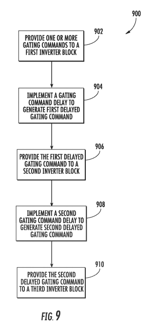
[0065] Referring now to FIG. 9, an example control method (900) for
operating a
converter according to example aspects of the present disclosure is depicted.
A
converter can include a plurality of inverter blocks. Each inverter block can
include
one or more SiC MOSFETS. For example, each inverter block can be a DC to DC to
AC inverter block, which can include a first conversion entity, a second
conversion
entity, a third conversion entity, and an isolation transformer. Each inverter
block can
include a plurality of switching devices, which can be one or more SiC
MOSFETS.
19
CA 03097955 2020-10-21
WO 2019/212453
PCT/US2018/030083
The converter can be, for example, a line side converter 168 in a wind power
generation system 100.
[0066] At (902), the control method (900) can include providing, by a
control
system, one or more gating commands to a first inverter block in the plurality
of
inverter blocks. For example, a first gating command 502A/802A can be provided
by
a control device 174 to a first gate drive card 402A associated with a first
inverter
block 206A. The first gate drive card 402A can be configured to drive the one
or
more switching devices, such as one or more SiC MOSFETs, in the first inverter
block 206A.
[0067] At (904), the control method (900) can include implementing a gating
command delay to generate a first delayed gating command based at least in
part on
the one or more gating commands. For example, a first gate drive card 402A can
be
configured to implement a gating command delay, such as a delay of 1-2
microseconds, to generate a first delayed gating command 502B. Further, a
gating
command delay can be a delay configured to generate a phase shift in a fixed
pulse
output for an inverter block. For example, a gating command delay can be
implemented to generate a second gating command 802B shifted by a phase shift
P.
[0068] At (906), the control method (900) can include providing the first
delayed
gating command to a second inverter block in the plurality of inverter blocks.
For
example, a first gate drive card 402A associated with a first inverter block
206A can
provide the first delayed gating command 502B/802B to a first gate drive card
402B
associated with a second inverter block 206B. The first gate drive card 402B
can then
provide the first delayed gating command 502B/802B to the second inverter
block
206B. In an embodiment, the first gate drive card 402A associated with the
first
inverter block 206A and the first gate drive card 402B associated with the
second
inverter block 206B can be arranged in a daisy chain configuration.
[0069] At (908), the control method (900) can include implementing a gating
command delay to generate a second delayed gating command based at least in
part
on first delayed gating command. For example, a first gate drive card 402B can
be
configured to implement a second gating command delay, such as a delay of 1-2
microseconds, to generate a second delayed gating command 502C. Further, a
gating
command delay can be a delay configured to generate a second phase shift in a
fixed
CA 03097955 2020-10-21
WO 2019/212453
PCT/US2018/030083
pulse output for an inverter block. For example, a gating command delay can be
implemented to generate a third gating command 802C shifted by a phase shift
P.
[0070] At (910), the control method (900) can include providing the second
delayed gating command to a third inverter block in the plurality of inverter
blocks.
For example, a first gate drive card 402B associated with a second inverter
block
206B can provide the second delayed gating command 502C/802C to a first gate
drive
card 402C associated with a third inverter block 206C. The first gate drive
card 402C
can then provide the first delayed gating command 502C/802C to the third
inverter
block 206C. In an embodiment, the first gate drive card 402B associated with
the
second inverter block 206B and the first gate drive card 402C associated with
the
third inverter block 206C can be arranged in a daisy chain configuration.
[0071] FIG. 10 depicts an example control device 1000 according to example
aspects of the present disclosure. The control device 1000 can be used, for
example,
as a control device 174 or a control system 176 in a wind power generation
system
100. The control device 1000 can include one or more computing device(s) 1100.
The computing device(s) 1100 can include one or more processor(s) 1100A and
one
or more memory device(s) 1100B. The one or more processor(s) 1100A can include
any suitable processing device, such as a microprocessor, microcontrol device,
integrated circuit, logic device, and/or other suitable processing device. The
one or
more memory device(s) 1100B can include one or more computer-readable media,
including, but not limited to, non-transitory computer-readable media, RAM,
ROM,
hard drives, flash drives, and/or other memory devices.
[0072] The one or more memory device(s) 1100B can store information
accessible by the one or more processor(s) 1100A, including computer-readable
instructions 1100C that can be executed by the one or more processor(s) 1100A.
The
instructions 1100C can be any set of instructions that when executed by the
one or
more processor(s) 1100A, cause the one or more processor(s) 1100A to perform
operations. In some embodiments, the instructions 1100C can be executed by the
one
or more processor(s) 1100A to cause the one or more processor(s) 1100A to
perform
operations, such as any of the operations and functions for which the
computing
system 1000 and/or the computing device(s) 1100 are configured, the operations
for
controlling a converter (e.g., control method 900), as described herein,
and/or any
21
CA 03097955 2020-10-21
WO 2019/212453
PCT/US2018/030083
other operations or functions of the one or more computing device(s) 1100. The
instructions 1100C can be software written in any suitable programming
language or
can be implemented in hardware. Additionally, and/or alternatively, the
instructions
1100C can be executed in logically and/or virtually separate threads on
processor(s)
1100A. The memory device(s) 1100B can further store data 1100D that can be
accessed by the processor(s) 1100A. For example, the data 1100D can include
data
indicative of power flows, current flows, temperatures, actual voltages,
nominal
voltages, gating commands, switching patterns, and/or any other data and/or
information described herein.
[0073] The computing device(s) 1100 can also include a network interface
1100E
used to communicate, for example, with the other components of system 1000
(e.g.,
via a network). The network interface 1100E can include any suitable
components for
interfacing with one or more network(s), including for example, transmitters,
receivers, ports, control devices, antennas, and/or other suitable components.
For
example, the network interface 1100E can be configured to communicate with one
or
more sensors in a wind power generation system 100, such as one or more
voltage
sensors or temperature sensors. Further, the network interface 1100 can be
configured
to communicate with a control system, such as a control system 176, or control
device, such as a control device 174.
[0074] The technology discussed herein makes reference to computer-based
systems and actions taken by and information sent to and from computer-based
systems. One of ordinary skill in the art will recognize that the inherent
flexibility of
computer-based systems allows for a great variety of possible configurations,
combinations, and divisions of tasks and functionality between and among
components. For instance, processes discussed herein can be implemented using
a
single computing device or multiple computing devices working in combination.
Databases, memory, instructions, and applications can be implemented on a
single
system or distributed across multiple systems. Distributed components can
operate
sequentially or in parallel.
[0075] The present disclosure is discussed with reference to DFIG power
generation systems including a power converter utilizing SiC MOSFETs for
purposes
of illustration and discussion. Those of ordinary skill in the art, using the
disclosures
22
CA 03097955 2020-10-21
WO 2019/212453
PCT/US2018/030083
provided herein, will understand that other power generation systems and/or
topologies can benefit from example aspects of the present disclosure. For
instance,
the grounding and protection schemes disclosed herein can be used in a wind,
solar,
gas turbine, or other suitable power generation system. Although specific
features of
various embodiments may be shown in some drawings and not in others, this is
for
convenience only. In accordance with the principles of the present disclosure,
any
feature of a drawing may be referenced and/or claimed in combination with any
feature of any other drawing.
[0076] This written description uses examples to disclose the invention,
including
the best mode, and also to enable any person skilled in the art to practice
the
invention, including making and using any devices or systems and performing
any
incorporated methods. The patentable scope of the invention is defined by the
claims,
and may include other examples that occur to those skilled in the art. Such
other
examples are intended to be within the scope of the claims if they include
structural
elements that do not differ from the literal language of the claims, or if
they include
equivalent structural elements with insubstantial differences from the literal
languages
of the claims.
23