Note: Descriptions are shown in the official language in which they were submitted.
CA 03098438 2020-10-26
FP19-0197-00
[0003] Patent Literature 1: US Patent No. 4112325
Patent Literature 2: Japanese Unexamined Patent Publication
No. H8-12772
Summary of Invention
Technical Problem
[0004] However, in the first-stage dynode described in Patent Literature
1, since the electron emission surface is formed by the flat bottom
surface having a teacup shape, it is difficult to adjust the transit time of
secondary electrons from the first-stage dynode to the second-stage
dynode. As a result, there may be a difference in the transit time of
secondary electrons from the first-stage dynode to the second-stage
dynode. In addition, in the first-stage dynode described in Patent
Literature 2, since a pair of side surfaces are provided on both sides of
the electron emission surface so as to be perpendicular to the electron
emission surface, secondary electrons emitted from the central region on
the electron emission surface travel linearly, while secondary electrons
emitted from a region in the vicinity of the side surface on the electron
emission surface may repel the side surface with the same electric
potential to travel. As a result, there may be a difference in the transit
time of secondary electrons from the first-stage dynode to the
second-stage dynode. Therefore, in the first-stage dynodes described
in Patent Literatures 1 and 2, it is expected that it is difficult to suppress
the cathode transit time difference (C. T. T. D) and the transit time
spread (T. T. S.) in the photomultiplier tube.
[0005] Therefore, it is an object of the present disclosure to provide a
first-stage dynode capable of suppressing a cathode transit time
2
Date Recue/Date Received 2020-10-26
CA 03098438 2020-10-26
FP19-0197-00
difference and a transit time spread in a photomultiplier tube and a
photomultiplier tube including such a first-stage dynode.
Solution to Problem
[0006] A first-stage dynode according to one aspect of the present
disclosure is a first-stage dynode to be used in a photomultiplier tube,
and includes: a bottom wall portion; and a pair of side wall portions
extending from both end portions of the bottom wall portion in a
predetermined direction to one side. An electron emission surface is
formed by a bottom surface of the bottom wall portion on the one side
and a pair of side surfaces of the pair of side wall portions on the one
side, and each of the pair of side surfaces is a curved surface that is
curved in a concave shape in a cross section parallel to the
predetermined direction.
[0007] In this first-stage dynode, each of the pair of side surfaces is a
curved surface that is curved in a concave shape in a cross section
parallel to the predetermined direction. Therefore, as each side surface
becomes farther from the center of the electron emission surface in the
predetermined direction, the side surface becomes closer to one electron
passage opening. As a result, both the transit distance of the
photoelectrons incident on each side surface and the transit distance of
the secondary electrons emitted from each side surface become shorter
as each side surface becomes closer to one electron passage opening.
Therefore, according to this first-stage dynode, it is possible to suppress
the cathode transit time difference and the transit time spread in the
photomultiplier tube.
[0008] In the first-stage dynode according to one aspect of the present
3
Date Recue/Date Received 2020-10-26
CA 03098438 2020-10-26
FP19-0197-00
disclosure, a radius of curvature of each of the pair of side surfaces may
be greater than 2 mm. According to this configuration, it is possible to
suitably suppress the cathode transit time difference and the transit time
spread in the photomultiplier tube.
[0009] In the first-stage dynode according to one aspect of the present
disclosure, assuming that a width of the electron emission surface in the
predetermined direction is L and a radius of curvature of each of the pair
of side surfaces is R, R 0.1L may be satisfied. According to this
configuration, it is possible to suitably suppress the cathode transit time
difference and the transit time spread in the photomultiplier tube.
[0010] In the first-stage dynode according to one aspect of the present
disclosure, the bottom surface may be a curved surface that is curved in
a concave shape in a cross section perpendicular to the predetermined
direction. According to this configuration, it becomes easy to adjust
the transit time of the secondary electrons from the first-stage dynode to
the second-stage dynode. Therefore, it is possible to suppress the
cathode transit time difference and the transit time spread more reliably
in the photomultiplier tube.
[0011] In the first-stage dynode according to one aspect of the present
disclosure, the electron emission surface may face one electron passage
opening. According to this configuration, since both the
photoelectrons incident on the electron emission surface and the
secondary electrons emitted from the electron emission surface pass
through one (that is, the same) electron passage opening 11b, the
dependence of the cathode transit time on the incidence position of
photoelectrons is reduced. Therefore, it is possible to suppress the
4
Date Recue/Date Received 2020-10-26
CA 03098438 2020-10-26
FP19-0197-00
cathode transit time difference and the transit time spread more reliably
in the photomultiplier tube.
[0012] A photomultiplier tube according to one aspect of the present
disclosure includes: a photocathode; a plurality of stages of dynodes;
and an anode. The plurality of stages of dynodes include a first-stage
dynode and a second-stage dynode arranged on a predetermined plane.
The first-stage dynode includes: a bottom wall portion; and a pair of
side wall portions extending from both end portions of the bottom wall
portion in a predetermined direction to the photocathode side and the
second-stage dynode side, the predetermined direction being
perpendicular to the predetermined plane. In the first-stage dynode, an
electron emission surface is formed by a bottom surface of the bottom
wall portion on the photocathode side and the second-stage dynode side
and a pair of side surfaces of the pair of side wall portions on the
photocathode side and the second-stage dynode side. Each of the pair
of side surfaces is a curved surface that is curved in a concave shape in a
cross section parallel to the predetermined direction.
[0013] According to this photomultiplier tube, it is possible to suppress
the cathode transit time difference and the transit time spread for the
reasons described above.
Advantageous Effects of Invention
[0014] According to the present disclosure, it is possible to provide a
first-stage dynode capable of suppressing a cathode transit time
difference and a transit time spread in a photomultiplier tube and a
photomultiplier tube including such a first-stage dynode.
Brief Description of Drawings
5
Date Recue/Date Received 2020-10-26
CA 03098438 2020-10-26
FP19-0197-00
[0015] FIG 1 is a cross-sectional view of a photomultiplier tube
according to an embodiment.
FIG 2 is a cross-sectional view of an electron multiplier and an
anode shown in FIG 1.
FIG 3 is a perspective view of a first-stage dynode according to
one embodiment.
FIG 4 is a cross-sectional view of the first-stage dynode taken
along line IV-IV shown in FIG 3.
FIG 5 is a cross-sectional view of the first-stage dynode taken
along line V-V shown in FIG 3.
FIG 6 is a perspective view of a first-stage dynode as a
comparative example.
FIG 7 is a schematic diagram for describing the traveling
trajectory of electrons.
FIG 8 is a diagram showing a cathode transit time difference
and a transit time spread in a photomultiplier tube using a first-stage
dynode as a first example.
FIG 9 is a diagram showing a cathode transit time difference
and a transit time spread in a photomultiplier tube using a first-stage
dynode as a second example.
FIG 10 is a diagram showing a cathode transit time difference
and a transit time spread in a photomultiplier tube using a first-stage
dynode as a third example.
FIG 11 is a diagram showing a cathode transit time difference
and a transit time spread in a photomultiplier tube using a first-stage
dynode as a fourth example.
6
Date Recue/Date Received 2020-10-26
CA 03098438 2020-10-26
FP19-0197-00
FIG 12 is a diagram showing a cathode transit time difference in
a photomultiplier tube using a first-stage dynode as a first comparative
example and a photomultiplier tube using a first-stage dynode as a fifth
example.
Description of Embodiments
[0016] Hereinafter, embodiments of the present disclosure will be
described in detail with reference to the diagrams. In addition, the
same or equivalent portions in the diagrams are denoted by the same
reference numerals, and repeated description thereof will be omitted.
[Configuration of photomultiplier tube]
[0017] As shown in FIG 1, a photomultiplier tube 1 includes a tube
body 2, a photocathode 3, an acceleration electrode 4, a focusing
electrode 5, an electron multiplier 6, and an anode 7. The electron
multiplier 6 has a plurality of stages (for example, 10 stages) of dynodes
10. In the following description, it is assumed that the side on which
light is incident on the photomultiplier tube 1 is "front" and the opposite
side is "rear". In addition, it is assumed that the tube axis (central axis)
of the tube body 2 is a "Z axis", an axis perpendicular to a plane (a plane
including the Z axis) on which the plurality of stages of dynodes 10 are
arranged is an "X axis", and an axis perpendicular to the Z axis and the
X axis is a "Y axis".
[0018] In the tube body 2, the photocathode 3, the acceleration
electrode 4, the focusing electrode 5, the electron multiplier 6, and the
anode 7 are housed in a vacuumed space. The tube body 2 is a
light-transmissive glass bulb. The tube body 2 has an oblate portion 2a
having the Z axis as its central axis and a cylindrical portion 2b having
7
Date Recue/Date Received 2020-10-26
CA 03098438 2020-10-26
FP19-0197-00
the Z axis as its central axis on the rear side of the oblate portion 2a.
The oblate portion 2a and the cylindrical portion 2b are integrally
formed as one glass bulb. As an example, the outer diameter of the
oblate portion 2a is about 200 mm and the outer diameter of the
cylindrical portion 2b is about 85 mm when viewed from the front side.
[0019] The photocathode 3 is provided on the inner surface of the tube
body 2. Specifically, the photocathode 3 is provided on the inner
surface of the front half region of the oblate portion 2a. The
photocathode 3 forms a transmissive photocathode, and is formed of, for
example, a potassium cesium antimonide/cesium type (bialkali) material
or other known materials. When light is incident on the photocathode
3 from the front side, photoelectrons are emitted from the photocathode
3 to the rear side by the photoelectric effect. As an example, the outer
diameter of the photocathode 3 when viewed from the front side (that is,
the effective diameter of the photomultiplier tube 1) is about 200 mm.
In addition, broken lines shown in FIG 1 indicate the trajectories
(representative trajectories) of the photoelectrons emitted from the
photocathode 3.
[0020] The acceleration electrode 4 is disposed behind the
photocathode 3. A predetermined voltage is applied to the acceleration
electrode 4. The acceleration electrode 4 is configured to accelerate
the photoelectrons emitted from the photocathode 3 toward the electron
multiplier 6. The focusing electrode 5 is disposed behind the
acceleration electrode 4. A predetermined voltage is applied to the
focusing electrode 5. The focusing electrode 5 is configured to focus
the photoelectrons emitted from the photocathode 3 toward the electron
8
Date Recue/Date Received 2020-10-26
CA 03098438 2020-10-26
FP19-0197-00
multiplier 6.
[0021] The electron multiplier 6 is disposed behind the focusing
electrode 5. The dynodes 10 in a plurality of stages are arranged on a
YZ plane (a plane including the Y axis and the Z axis). Each dynode
10 is formed of, for example, stainless steel. A predetennined voltage
is applied to each of the plurality of stages of dynodes 10. The
electron multiplier 6, that is, the plurality of stages of dynodes 10 are
configured to multiply the photoelectrons emitted from the
photocathode 3. The anode 7 is disposed on the YZ plane so as to face
the final-stage dynode 10. A predetermined voltage is applied to the
anode 7. The anode 7 is configured to output the secondary electrons
emitted from the final-stage dynode 10 as a signal current.
[0022] The acceleration electrode 4, the focusing electrode 5, the
dynodes 10 of the electron multiplier 6, and the anode 7 are supported
by a support member (not shown) in the tube body 2. The support
member is attached to a stem (not shown) that seals a rear end portion of
the cylindrical portion 2b. In addition, in the stem, a wiring for voltage
application and a wiring for signal current output are provided as a stem
pin or a cable.
[Structure of electron multiplier]
[0023] As shown in FIG 2, in the electron multiplier 6, the plurality of
stages of dynodes 10 include a first-stage dynode 11, a second-stage
dynode 12, and a third-stage dynode 13. In the following description,
respective dynodes including the first-stage dynode 11, the second-stage
dynode 12, and the third-stage dynode 13 are collectively referred to as
a dynode 10. In addition, electron emission surfaces of the respective
9
Date Recue/Date Received 2020-10-26
CA 03098438 2020-10-26
FP19-0197-00
dynodes including an electron emission surface 11a of the first-stage
dynode 11, an electron emission surface 12a of the second-stage dynode
12, and an electron emission surface 13a of the third-stage dynode 13
are collectively referred to as an electron emission surface 10a.
[0024] The first-stage dynode 11 is disposed such that the electron
emission surface ha faces the photocathode 3 (see FIG 1) and the
electron emission surface 12a of the second-stage dynode 12. The
second-stage dynode 12 is disposed such that the electron emission
surface 12a faces the electron emission surface 11a of the first-stage
dynode 11 and the electron emission surface 13a of the third-stage
dynode 13. Similarly, each of the dynodes 10 in the third and
subsequent stages excluding the final-stage dynode 10 is disposed such
that its electron emission surface 10a faces the electron emission surface
10a of the dynode 10 in the previous stage and the electron emission
surface 10a of the dynode 10 in the later stage. The final-stage dynode
10 is disposed such that its electron emission surface 10a faces the
electron emission surface 10a of the dynode 10 in the previous stage and
the anode 7.
[0025] The first-stage dynode 11 has a bottom wall portion 111, a pair
of side wall portions 112, a first holding portion 113, and a pair of
second holding portions 114 (details thereof will be described later).
The electron emission surface ha of the first-stage dynode 11 is formed
by the bottom surface of the bottom wall portion 111 on the
photocathode 3 side and the second-stage dynode 12 side and a pair of
side surfaces of the pair of side wall portions 112 on the photocathode 3
side and the second-stage dynode 12 side.
Date Recue/Date Received 2020-10-26
CA 03098438 2020-10-26
FP19-0197-00
[0026] The second-stage dynode 12 has a bottom wall portion 121 and
a pair of holding portions 122. The electron emission surface 12a of
the second-stage dynode 12 is formed by the bottom surface of the
bottom wall portion 121 on the first-stage dynode 11 side and the
third-stage dynode 13 side. The pair of holding portions 122 extend
from both end portions of the bottom wall portion 121 in the X-axis
direction (direction parallel to the X axis) to the first-stage dynode 11
side and the third-stage dynode 13 side.
[0027] The third-stage dynode 13 has a bottom wall portion 131 and a
pair of holding portions 132. The electron emission surface 13a of the
third-stage dynode 13 is formed by the bottom surface of the bottom
wall portion 131 on the second-stage dynode 12 side and the
fourth-stage dynode 10 side. The pair of holding portions 132 extend
from both ends of the bottom wall portion 131 in the X-axis direction to
the second-stage dynode 12 side and the fourth-stage dynode 10 side.
[0028] A pair of electron lens forming electrodes 14 are provided in a
region between the first-stage dynode 11, the second-stage dynode 12,
and the third-stage dynode 13. Specifically, one electron lens forming
electrode 14 is formed integrally with the one holding portion 132 so as
to extend in a region between the one second holding portion 114 and
the one holding portion 122. The other electron lens forming electrode
14 is formed integrally with the other holding portion 132 so as to
extend in a region between the other second holding portion 114 and the
other holding portion 122. A predetermined voltage applied to the
third-stage dynode 13 is applied to the pair of electron lens forming
electrodes 14. As a result, the electric potential distribution in the
11
Date Recue/Date Received 2020-10-26
CA 03098438 2020-10-26
FP19-0197-00
X-axis direction is made flat in a region between the first-stage dynode
11 and the second-stage dynode 12.
[Configuration of first-stage dynode]
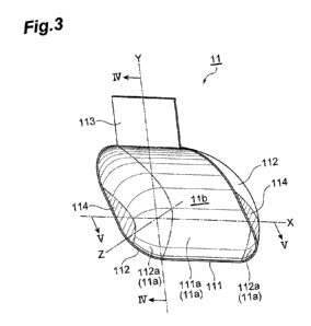
[0029] As shown in FIGS. 3, 4, and 5, the first-stage dynode 11
includes the bottom wall portion 111, a pair of side wall portions 112,
the first holding portion 113, and a pair of second holding portions 114.
The pair of side wall portions 112 extend from both end portions of the
bottom wall portion 111 in the X-axis direction (predetermined direction
perpendicular to a predetermined plane) to one side (the photocathode 3
side and the second-stage dynode 12 side (see FIGS. 1 and 2)). The
first holding portion 113 extends outward (on a side opposite to the
second-stage dynode (see FIGS. 1 and 2)) from the end portion of the
bottom wall portion 111 on the front side (photocathode 3 side (see
FIGS. 1 and 2)). The pair of second holding portions 114 extend from
both end portions of the pair of side wall portions 112 in the X-axis
direction to one side.
[0030] The first holding portion 113 has a flat plate shape (for example,
a rectangular plate shape) parallel to the XY plane. Each of the pair of
second holding portions 114 has a flat plate shape parallel to the YZ
plane. The first-stage dynode 11 is attached to a support member
provided in the tube body 2 through the first holding portion 113 and the
pair of second holding portions 114.
[0031] The electron emission surface lla of the first-stage dynode 11 is
formed by a bottom surface 111a of the bottom wall portion 111 on one
side and a pair of side surfaces 112a of the pair of side wall portions 112
on one side. The electron emission surface 1 1 a faces one electron
12
Date Recue/Date Received 2020-10-26
CA 03098438 2020-10-26
FP19-0197-00
passage opening 11b. In the first-stage dynode 11, one electron
passage opening 1 lb is defined by the bottom wall portion 111, the pair
of side wall portions 112, and edge portions of the pair of second
holding portions 114 on one side. That is, both the photoelectrons
incident on the electron emission surface lla and the secondary
electrons emitted from the electron emission surface lla pass through
one (that is, the same) electron passage opening 11b.
[0032] The bottom surface 111a forming the electron emission surface
lla is a curved surface that is curved in a concave shape in a cross
section perpendicular to the X-axis direction (see particularly FIG 4).
In the present embodiment, the bottom surface 111a is a cylindrical
surface (elliptic cylindrical surface, hyperbolic cylindrical surface,
parabolic cylindrical surface, composite surface thereof, and the like)
having the X-axis direction as its longitudinal direction (cylinder height
direction). Each of the pair of side surfaces 112a forming the electron
emission surface lla is a curved surface that is curved in a concave
shape in a cross section parallel to the X-axis direction (see particularly
FIG 5). In the present embodiment, each side surface 112a
corresponds to a chamfered surface when a round inner chamfer is
applied to a corner portion formed by the bottom surface 111a and the
inner surface of each second holding portion 114. In addition, the
bottom surface 111a and each side surface 112a are connected to each
other so that the curvatures are continuous. In addition, each side
surface 112a and the inner surface of each second holding portion 114
are also connected to each other so that the curvatures are continuous.
[0033] Assuming that the width of the electron emission surface 1 la in
13
Date Recue/Date Received 2020-10-26
CA 03098438 2020-10-26
FP19-0197-00
the X-axis direction is L and the radius of curvature of each of the pair
of side surfaces 112a is R (see FIG 5), R 0.1L is satisfied in the
first-stage dynode 11. In addition, the radius of curvature R of each of
the pair of side surfaces 112a is greater than 2 mm. As an example, the
width L of the electron emission surface lla in the X-axis direction is
greater than 20 mm and smaller than 50 mm.
[0034] The first-stage dynode 11 having the above-described shape is
integrally formed by a metal plate (for example, a stainless steel plate
having a thickness of about 0.3 mm). That is, the bottom wall portion
111, the pair of side wall portions 112, the first holding portion 113, and
the pair of second holding portions 114 are integrally formed by a metal
plate. Here, being integrally formed by the metal plate means being
formed by performing plastic working, such as press working, on the
metal plate.
[Operations and effects]
[0035] In the first-stage dynode 11, each of the pair of side surfaces
112a forming the electron emission surface lla is a curved surface that
is curved in a concave shape in a cross section parallel to the X-axis
direction. Therefore, as each side surface 112a becomes farther from
the center of the electron emission surface lla in the X-axis direction,
the side surface 112a becomes closer to one electron passage opening
11b. As a result, both the transit distance of the photoelectrons
incident on each side surface 112a and the transit distance of the
secondary electrons emitted from each side surface 112a become shorter
as each side surface 112a becomes closer to one electron passage
opening 11b. Therefore, according to the first-stage dynode 11, it is
14
Date Recue/Date Received 2020-10-26
CA 03098438 2020-10-26
FP19-0197-00
possible to suppress the cathode transit time difference and the transit
time spread in the photomultiplier tube 1.
[0036] In addition, even if the entire electron emission surface is
formed in a spherical shape, for example, in the first-stage dynode
having such an electron emission surface, it is difficult to adjust the
transit time of the secondary electrons from the first-stage dynode to the
second-stage dynode. Therefore, it is difficult to effectively suppress
the cathode transit time difference and the transit time spread in the
photomultiplier tube. In addition, in order to suppress the cathode
transit time difference and the transit time spread, it may be considered
that the electron emission surface is formed only by the bottom surface
111a without providing the pair of side surfaces 112a to increase the
width of the electron emission surface in the X-axis direction.
However, in the first-stage dynode having such an electron emission
surface, since the size is large, the outer diameter of the cylindrical
portion 2b of the tube body 2 should be made large. Therefore, it is
difficult to secure the water pressure resistance of the tube body 2. In
addition, when the size of the first-stage dynode increases, it is difficult
to form the first-stage dynode by performing plastic working, such as
press working, on the metal plate. According to the first-stage dynode
11 described above, it is possible to suppress the cathode transit time
difference and the transit time spread in the photomultiplier tube 1 while
suppressing an increase in the size thereof.
[0037] In addition, in the first-stage dynode 11, the radius of curvature
R of each of the pair of side surfaces 112a is greater than 2 mm. With
this configuration, it is possible to suitably suppress the cathode transit
Date Recue/Date Received 2020-10-26
CA 03098438 2020-10-26
FP19-0197-00
time difference and the transit time spread in the photomultiplier tube 1.
[0038] In addition, in the first-stage dynode 11, assuming that the width
of the electron emission surface lla in the X-axis direction is L and the
radius of curvature of each of the pair of side surfaces 112a is R, R
0.1L is satisfied. With this configuration, it is possible to suitably
suppress the cathode transit time difference and the transit time spread
in the photomultiplier tube 1.
[0039] In addition, in the first-stage dynode 11, the bottom surface 111a
forming the electron emission surface lla is a curved surface that is
curved in a concave shape in a cross section perpendicular to the X-axis
direction. With this configuration, it becomes easy to adjust the transit
time of the secondary electrons from the first-stage dynode 11 to the
second-stage dynode 12. Therefore, it is possible to suppress the
cathode transit time difference and the transit time spread more reliably
in the photomultiplier tube 1.
[0040] In addition, in the first-stage dynode 11, the electron emission
surface 1 1 a faces one electron passage opening 11b. With this
configuration, since both the photoelectrons incident on the electron
emission surface ha and the secondary electrons emitted from the
electron emission surface ha pass through one (that is, the same)
electron passage opening 11b, the dependence of the cathode transit
time on the incidence position of photoelectrons is reduced. Therefore,
it is possible to suppress the cathode transit time difference and the
transit time spread more reliably in the photomultiplier tube 1.
[0041] Here, the reason why a difference in the transit time of
secondary electrons up to the second-stage dynode 12 is unlikely to
16
Date Recue/Date Received 2020-10-26
CA 03098438 2020-10-26
FP19-0197-00
occur in the first-stage dynode 11 described above will be described in
more detail.
[0042] FIG 6 is a perspective view of a first-stage dynode 15 as a
comparative example. As shown in FIG 6, the first-stage dynode 15
as a comparative example is mainly different from the first-stage
dynode 11 described above in that the pair of side wall portions 112 are
not provided and the pair of second holding portions 114 cross the
bottom wall portion 111. In the first-stage dynode 15 as a comparative
example, an electron emission surface 15a facing one electron passage
opening 15b is formed by the bottom surface 111a.
[0043] In the first-stage dynode 15 as a comparative example, as shown
in (a) of FIG 7, secondary electrons that are emitted from the central
region of the electron emission surface 15a due to photoelectrons being
incident on the central region along a trajectory Al travel linearly along
a trajectory Bl. Meanwhile, secondary electrons that are emitted from
a region in the vicinity of the second holding portion 114 on the electron
emission surface 15a due to photoelectrons being incident on the
vicinity region along a trajectory A2 repel the second holding portion
114 with the same electric potential to travel along a trajectory B2. As
a result, in the first-stage dynode 15 as a comparative example, a
difference in the transit time of the secondary electrons up to the
second-stage dynode 12 is likely to occur.
[0044] On the other hand, in the first-stage dynode 11 described above,
as shown in (b) of FIG 7, secondary electrons that are emitted from the
central region of the electron emission surface lla due to photoelectrons
being incident on the central region along the trajectory Al travel
17
Date Recue/Date Received 2020-10-26
CA 03098438 2020-10-26
FP19-0197-00
linearly along the trajectory Bl. Meanwhile, secondary electrons that
are emitted from a region (that is, the side surface 112a) in the vicinity
of the second holding portion 114 on the electron emission surface ha
due to photoelectrons being incident on the vicinity region along the
trajectory A2 repel the second holding portion 114 with the same
electric potential to travel along the trajectory B2, but both the transit
distance of the photoelectrons incident on the vicinity region and the
transit distance of the secondary electrons emitted from the vicinity
region become shorter as the side surface 112a becomes closer to the
electron passage opening 11b. As a result, in the first-stage dynode 11
described above, a difference in the transit time of secondary electrons
up to the second-stage dynode 12 is unlikely to occur.
[0045] Next, the reason why it is more preferable that the radius of
curvature R of each of the pair of side surfaces 112a forming the
electron emission surface lla is greater than 2 mm in the first-stage
dynode 11 will be described together with the simulation result.
[0046] First, as a simulation model, a first-stage dynode as a first
example, a first-stage dynode as a second example, a first-stage dynode
as a third example, and a first-stage dynode as a fourth example were
prepared. Each first-stage dynode corresponds to one formed by
pressing a stainless steel plate having a thickness of 0.3 mm. In each
of the first-stage dynodes, the width L of the electron emission surface
in the X-axis direction was 30.6 mm.
[0047] The respective first-stage dynodes have the same configuration
as the above-described first-stage dynode 11, but are different from each
other only in the following point. That is, the radius of curvature R
18
Date Recue/Date Received 2020-10-26
CA 03098438 2020-10-26
FP19-0197-00
was 2 mm in the first-stage dynode as the first example, the radius of
curvature R was 4 mm in the first-stage dynode as the second example,
the radius of curvature R was 6 mm in the first-stage dynode as the third
example, and the radius of curvature R was 8 mm in the first-stage
dynode as the fourth example.
[0048] In a simulation corresponding to a case where the first-stage
dynode as the first example, the first-stage dynode as the second
example, the first-stage dynode as the third example, and the first-stage
dynode as the fourth example were attached to the same photomultiplier
tube and the photomultiplier tube was operated under the same
conditions, the cathode transit time difference and the transit time
spread in the X-axis direction were measured.
[0049] (a) of FIG 8 is a diagram showing a cathode transit time
difference in a photomultiplier tube using the first-stage dynode as the
first example, and (b) of FIG 8 is a diagram showing a transit time
spread in that case. (a) of FIG 9 is a diagram showing a cathode
transit time difference in a photomultiplier tube using the first-stage
dynode as the second example, and (b) of FIG 9 is a diagram showing a
transit time spread in that case. (a) of FIG 10 is a diagram showing a
cathode transit time difference in a photomultiplier tube using the
first-stage dynode as the third example, and (b) of FIG 10 is a diagram
showing a transit time spread in that case. (a) of FIG 11 is a diagram
showing a cathode transit time difference in a photomultiplier tube
using the first-stage dynode as the fourth example, and (b) of FIG 11 is
a diagram showing a transit time spread in that case.
[0050] As shown in (a) of FIGS. 8, 9, 10, and 11, in the first-stage
19
Date Recue/Date Received 2020-10-26
CA 03098438 2020-10-26
FP19-0197-00
dynode as the second example, the first-stage dynode as the third
example, and the first-stage dynode as the fourth example, the cathode
transit time difference in the X-axis direction was made more uniform at
both end portions in the X-axis direction, compared with the
photomultiplier tube using the first-stage dynode as the first example.
In addition, as shown in (b) of FIGS. 8, 9, 10, and 11, in the first-stage
dynode as the second example, the first-stage dynode as the third
example, and the first-stage dynode as the fourth example, the transit
time spread in the X-axis direction was further reduced compared with
the photomultiplier tube using the first-stage dynode as the first
example.
[0051] From the above simulation result, it can be said that it is more
preferable that the radius of curvature R of each of the pair of side
surfaces forming the electron emission surface is greater than 2 mm in
order to suppress the cathode transit time difference and the transit time
spread in the photomultiplier tube.
[0052] Next, the reason why it is more preferable that R 0.1L is
satisfied in the first-stage dynode 11 will be described together with the
simulation result.
[0053] From the simulation result described above, R 0.1L is not
satisfied in the first-stage dynode as the first example (L: 30.6 mm, R: 2
mm), and R 0.1L is satisfied in the first-stage dynode as the second
example (L: 30.6 mm, R: 4 mm), the first-stage dynode as the third
example (L: 30.6 mm, R: 6 mm), and the first-stage dynode as the
fourth example (L: 30.6 mm, R: 8 mm). Therefore, it was confirmed
by simulation that it could be said that satisfying R 0.1L in the
Date Recue/Date Received 2020-10-26
CA 03098438 2020-10-26
FP19-0197-00
first-stage dynode even if the width L of the electron emission surface in
the X-axis direction was not 30.6 mm was more preferable for
suppressing the cathode transit time difference and the transit time
spread in the photomultiplier tube.
[0054] First, as a simulation model, a first-stage dynode as a first
comparative example and a first-stage dynode as a fifth example were
prepared. Each first-stage dynode corresponds to one formed by
pressing a stainless steel plate having a thickness of 0.3 mm. In the
first-stage dynode as the first comparative example, the width L of the
electron emission surface in the X-axis direction was 34 mm, and the
radius of curvature R of each of a pair of side surfaces was 0 mm (that
is, the first-stage dynode as the first comparative example has the same
configuration as the first-stage dynode 15 shown in FIG 6). In the
first-stage dynode as the fifth embodiment, the width L of the electron
emission surface in the X-axis direction was 34 mm, and the radius of
curvature R of each of a pair of side surfaces was 5 mm (that is, the
first-stage dynode as the fifth example has the same configuration as the
first-stage dynode 11 described above).
[0055] In a simulation corresponding to a case where the first-stage
dynode as the first comparative example and the first-stage dynode as
the fifth example were attached to the same photomultiplier tube and the
photomultiplier tube was operated under the same conditions, the
cathode transit time difference in the X-axis direction was measured.
(a) of FIG 12 is a diagram showing a cathode transit time difference in a
photomultiplier tube using the first-stage dynode as the first
comparative example, and (b) of FIG 12 is a diagram showing a
21
Date Recue/Date Received 2020-10-26
CA 03098438 2020-10-26
FP19-0197-00
cathode transit time difference in a photomultiplier tube using the
first-stage dynode as the fifth example.
[0056] As shown in (a) and (b) of FIG 12, in the photomultiplier tube
using the first-stage dynode as the fifth example, the cathode transit
time difference in the X-axis direction was made uniform at both end
portions in the X-axis direction, compared with the photomultiplier tube
using the first-stage dynode as the first comparative example. From
this simulation result, it can be said that satisfying R 0.1L in the
first-stage dynode is more preferable for suppressing the cathode transit
time difference and the transit time spread in the photomultiplier tube.
[Modification examples]
[0057] The present disclosure is not limited to the embodiment
described above. For example, the material and shape of each
component are not limited to the materials and shapes described above,
and various materials and shapes can be adopted. As an example, the
first holding portion 113 is not limited to the rectangular plate shape,
and may have other shapes such as a semicircular plate shape. In
addition, the first-stage dynode 11 may not have the first holding
portion 113.
[0058] In addition, an edge portion of each of the pair of second
holding portions 114 on one side may be formed so as to protrude from
the bottom wall portion 111 and an edge portion of each of the pair of
side wall portions 112 on one side, or may be formed so as to be
recessed from the bottom wall portion 111 and an edge portion of each
of the pair of side wall portions 112 on one side. In addition, the
first-stage dynode 11 may not have the pair of second holding portions
22
Date Recue/Date Received 2020-10-26
CA 03098438 2020-10-26
FP19-0197-00
114. In this case, for example, a metal film having the same shape as
the second holding portion 114 may be formed on the surface of each of
a pair of substrates interposing the first-stage dynode 11 therebetween in
the X-axis direction by evaporation or the like, and the metal film may
be disposed in a portion where the second holding portion 114 is
missing.
[0059] In addition, a plurality of electron passage openings facing the
electron emission surface lla may be formed so that the photoelectrons
incident on the electron emission surface lla and the secondary
electrons emitted from the electron emission surface lla pass through
different electron passage openings. In addition, the bottom surface
111a forming the electron emission surface lla may include a flat
region.
[0060] In addition, the bottom wall portion 111, the pair of side wall
portions 112, the first holding portion 113, and the pair of second
holding portions 114 may not be formed in a plate shape. As an
example, the bottom wall portion 111, the pair of side wall portions 112,
the first holding portion 113, and the pair of second holding portions
114 may be formed in a block shape, and the electron emission surface
lla described above may be formed by cutting or the like.
Reference Signs List
[0061] 1: photomultiplier tube, 3: photocathode, 7: anode, 10: dynode,
11: first-stage dynode, ha: electron emission surface, 1 lb: electron
passage opening, 12: second-stage dynode, 111: bottom wall portion,
111a: bottom surface, 112: side wall portion, 112a: side surface.
23
Date Recue/Date Received 2020-10-26