Note: Descriptions are shown in the official language in which they were submitted.
87283705
ENERGY STORAGE MEDIA FOR ULTRA CAPACITORS
[0001] This application is a divisional of Canadian Patent Application Number
2,838,557 filed on
June 7, 2012.
BACKGROUND OF THE INVENTION
1. Field of the Invention
[0002] The invention generally relates to capacitors, and more specifically to
carbon nanotubes for
use therein.
2. Description of the Related Art
[0003] Carbon nanotubes (hereinafter referred to also as "CNTs") are carbon
structures that
exhibit a variety of properties. Many of the properties suggest opportunities
for improvements in a
variety of technologies. For example, technologies that benefit from increased
strength,
conductivity or capacitance will benefit from the use of CNT. Accordingly,
advances in CNT
technology are of great interest to those working with capacitors.
[0004] Capacitors are one of the key components in a variety of electric
systems. Functions
include power buffering, energy storage, and voltage smoothing. A variety of
industries present
demanding requirements for capacitors.
[0005] Consider, for example, that industries such as automotive,
manufacturing, aerospace,
aviation, medical, and military have some applications that require capacitors
to provide energy or
power support for electrified drive, pulse power, or process actuation. Energy
capacity and power
capability are key requirements in typical applications within those
industries. Applications such
as providing torque assist in electrified drivetrains, power-assist for motor
drives in manufacturing
plants, or voltage support during high power load demands, require substantial
energy and power.
Some applications present limited physical space or upper bounds on weight.
Some applications
require long cycle life.
[0006] Thus, capacitors used in industrial environments must meet demands for
performance
while meeting physical constraints. For designers and producers of
utlracapacitors, one of the
attendant challenges is obtaining an electrode that will function at a desired
output.
1
Date Recue/Date Received 2020-11-09
WO 2012/170749
PCT/US2012/041438
[0007] Thus, what are needed are methods and apparatus for production of a
high power
electrode based on carbon nanotubes. Preferably, the methods and apparatus are
simple to
perform and thus offer reduced cost of manufacture, as well as an improved
rate of
production. Preferably, the methods and apparatus provide for electrodes for
ultracapacitors
that perform well in demanding situations. Preferably, the electrodes provide
stable
conductivity and low internal resistance over a wide range of temperatures.
SUMMARY OF THE INVENTION
[0008] Methods and apparatus for fabrication of carbon nanotubes are provided.
The
methods and apparatus provide for carbon nanotubes that exhibit superior
characteristics, and
therefore performance when used in a variety of applications. A variety of
forms of
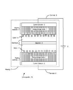
electrodes and ultracapacitors may be realized as a result.
[0009] In one embodiment, a method of producing an aggregate of vertically
aligned carbon
nanotubes is provided. The method includes loading a base material into a
substantially
oxygen free environment; disposing a catalyst onto the base material to
provide a substrate;
subjecting the substrate to a raw material gas and heating at least one of the
raw material gas
and the substrate for growing the aggregate onto the substrate; and cooling
the aggregate in a
substantially oxygen free environment.
[0010] In another embodiment, an apparatus for producing an aggregate of
vertically aligned
carbon nanotubes, is provided. The apparatus includes a loader section for
loading a base
material into a substantially oxygen free environment; a sputterer section for
disposing a
catalyst onto the base material to provide a substrate; a carbon deposition
section for
subjecting the substrate to a raw material gas and heating at least one of the
raw material gas
and the substrate for growing the aggregate onto the substrate; and a cooler
section for
cooling the aggregate in a substantially oxygen free environment.
[0011] In another embodiment, a method of producing an electrode for an
ultracapacitor, the
electrode including an aggregate of vertically aligned carbon nanotubes is
provided. The
method includes selecting aggregate that has been fabricated by loading a base
material into a
substantially oxygen free environment; disposing a catalyst onto the base
material to provide
a substrate; subjecting the substrate to a raw material gas and heating at
least one of the raw
material gas and the substrate to grow the aggregate thereon; cooling the
aggregate in a
substantially oxygen free environment; and one of joining the aggregate with a
current
collector, removing the aggregate from the substrate and disposing a current
collector onto
2
Date Recue/Date Received 2020-11-09
WO 2012/170749
PCT/US2012/041438
the aggregate and combining the aggregate with other carbonaceous material an
joining the
combination with a current collector.
[0012] In another embodiment, a method of producing an electrode for an energy
storage
system is provided. The method includes selecting a substrate including a
thickness of
vertically aligned carbon nanotubes (CNT) disposed thereon; disposing a
bonding layer onto
the thickness of CNT; bonding the bonding layer to a current collector; and
removing the
substrate from the CNT to provide the electrode.
[0013] In another embodiment, a method of producing an ultracapacitor, the
ultracapacitor
including at least one electrode including an aggregate of vertically aligned
carbon nanotubes
is provided. The method includes selecting an electrode that has been
fabricated by selecting
aggregate that has been fabricated by loading a base material into a
substantially oxygen free
environment; disposing a catalyst onto the base material to provide a
substrate; subjecting the
substrate to a raw material gas and heating at least one of the raw material
gas and the
substrate to grow the aggregate thereon; cooling the aggregate in a
substantially oxygen free
environment; and one of transferring the aggregate onto a current collector,
removing the
aggregate from the substrate and disposing a current collector onto the
aggregate and
combining the aggregate with other carbonaceous material on a current
collector to provide
the electrode; and incorporating the electrode into the ultracapacitor.
[0014] In another embodiment, a method of producing an electrode for an energy
storage
system is provided. The method includes selecting a base including a current
collector and a
first joining layer disposed over the current collector; and joining a second
joining layer to
the first joining layer, the second joining layer including a carbonaceous
layer disposed
thereon, the carbonaceous layer including material for storing charge.
[0015] In another embodiment, an electrode is provided. The electrode includes
a base
including a current collector and a first joining layer disposed over the
current collector; and
a second joining layer joined to the first joining layer, the second joining
layer including an
carbonaceous layer disposed thereon, the carbonaceous layer including material
for storing
charge.
[0016] In another embodiment, a capacitor is provided. The capacitor includes
a housing
including at least one electrode including a base including a current
collector and a first
joining layer disposed over the current collector; and a second joining layer
joined to the first
joining layer, the second joining layer including a carbonaceous layer
disposed thereon, the
3
Date Recue/Date Received 2020-11-09
WO 2012/170749
PCT/US2012/041438
carbonaceous layer including material for storing charge of the capacitor; and
at least one of
an electrolyte and a dielectric material disposed therein, the at least one
electrode coupled to
an output electrode of the housing.
[0017] In another embodiment, a method for providing a multi-form electrode
for an energy
storage device is provided. The method includes selecting an electrode
including an
aggregate of carbon nanotubes in electrical contact with a current collector;
disposing at least
one nanoform carbon dispersed in a carrier material onto the aggregate; and
expelling the
carrier material to provide the multi-form electrode.
[0018] In another embodiment, a multi-form electrode for an energy storage
device, the
multi-form electrode is provided. The electrode includes an aggregate of
carbon nanotubes
disposed over a current collector, the aggregate further including at least
one additional layer
of nanoform carbon having been disposed over the aggregate as a solution
including the
nanoform carbon disbursed in a carrier material.
[0019] In another embodiment, an ultracapacitor is provided. The
ultracapacitor includes a
housing including at least multi-form electrode disposed therein; the multi-
form electrode
including an aggregate of carbon nanotubes disposed over a current collector,
the aggregate
further including at least one additional layer of nanoform carbon having been
disposed over
the aggregate as a solution including the nanoform carbon disbursed in a
carrier material; and
an electrolyte for providing ionic transport within the ultracapacitor.
[0020] In another embodiment, a method for providing a carbonaceous aggregate
is provided.
The method includes dispersing an aggregate of aligned carbon nanotubes into a
first
solution; dispersing a carbon addition into a second solution; ultrasonically
mixing the first
solution and the second solution; combining the mixed first solution and the
mixed second
solution to provide a combined solution; ultrasonically mixing the combined
solution;
obtaining a carbonaceous aggregate from the mixed combined solution.
[0021] In another embodiment, an electrode with energy storage media that
includes a
carbonaceous aggregate is provided. The electrode includes a current collector
including the
carbonaceous aggregate disposed thereon, the aggregate including a combination
of sonicated
carbon nanoforms.
[0022] In another embodiment, an ultracapacitor is provided. The
ultracapacitor includes at
least one electrode with energy storage media that includes a carbonaceous
aggregate, the
4
Date Recue/Date Received 2020-11-09
WO 2012/170749
PCT/US2012/041438
electrode including a current collector including the carbonaceous aggregate
disposed
thereon, the aggregate including a combination of sonicated carbon nanoforms.
[0023] In another embodiment, a method for fabricating an element of electrode
is provided.
The method includes selecting a substrate including an aggregate of carbon
nanotubes
disposed thereon; depositing a layer of conductive material onto the
aggregate; and removing
the aggregate and conductive material from the substrate.
[0024] In another embodiment, an electrode is provided. The electrode includes
a plurality
of electrode elements, each element including an aggregate of carbon nanotubes
and a layer
of conductive material disposed thereon; each of the elements coupled to
another one of the
elements, at least one coupling including a bond to the conductive material of
the element.
[0025] In another embodiment, an ultracapacitor is provided. The
ultracapacitor includes at
least one electrode including a plurality of electrode elements, each element
including an
aggregate of carbon nanotubes and a layer of conductive material disposed
thereon; each of
the elements coupled to another one of the elements, at least one coupling
including a bond to
the conductive material of the element; a housing for containing the at least
one electrode;
and electrolyte for providing transport of ions within the ultracapacitor.
[0026] In another embodiment, a method for fabricating an electrode is
provided. The
method includes obtaining a layered stack of carbon nanotubes (CNT); wetting
the layered
stack with a solution; compressing the layered stack; drying the compressed
layered stack;
and applying a current collector to the compressed layered stack.
[0027] In another embodiment, an ultracapacitor is provided. The
ultracapacitor includes: at
least one electrode including a compressed layered stack of carbon nanotubes
(CNT) and a
current collector disposed onto the stack; and an electrolyte for transporting
energy stored in
the electrode to at least one terminal of the ultracapacitor.
[0028] In another embodiment, a method of using an ultracapacitor is provided.
The method
includes: obtaining an ultracapacitor comprising an electrolyte and two
electrodes, each of
the electrodes in electrical communication with a cuirent collector and
separated from the
other by a separator; and cycling the ultracapacitor by alternatively charging
and discharging
the ultracapacitor, wherein a power density output of the ultracapacitor is at
least 12 kW/kg
up to about 250kW/kg for each cycle.
[0029] In another embodiment, a method of using an ultracapacitor is provided.
The method
includes: obtaining an ultracapacitor comprising an electrolyte and two
electrodes, each of
Date Recue/Date Received 2020-11-09
87283705
the electrodes in electrical communication with a current collector and
separated from the
other by a separator; and cycling the ultracapacitor by alternatively charging
and discharging
the ultracapacitor, wherein an energy density output of the ultracapacitor is
at least 1 Wh/kg
up to about 35 Wh/kg for each cycle.
[0030] In another embodiment, a method of using an ultracapacitor is provided.
The method
includes: obtaining an ultracapacitor comprising an electrolyte and two
electrodes, each of the
electrodes in electrical communication with a current collector and separated
from the other
by a separator; and cycling the capacitor by alternatively charging and
discharging the
capacitor at least three times, while maintaining a voltage across the
ultracapacitor between a
maximum voltage and about half of the maximum voltage, wherein the charging
and
discharging provides an output from the ultracapacitor of at least 3.75 Wh/kg
of energy in a
single charge or discharge.
[0030a] According to one aspect of the present invention, there is provided an
apparatus
comprising: an electrode for an ultracapacitor, the electrode comprising: a
current collector
comprising a bonding layer disposed thereon, wherein the bonding layer is at
least one of
conductive, electrically inert, and compatible with material of the current
collector; and at
least one layer of compressed vertically aligned carbon nanotubes comprising a
bonding layer
disposed thereon, wherein the bonding layer of the current collector is bonded
to the bonding
layer of the layer of compressed vertically aligned carbon nanotubes, and
wherein the
electrode comprises another layer of carbon nanotubes on the at least one
layer of compressed
vertically aligned carbon nanotubes.
[0030b] According to another aspect of the present invention, there is
provided a method
comprising: forming an electrode for an ultracapacitor, said forming
comprising the steps of:
providing a current collector comprising a bonding layer disposed thereon,
wherein the
bonding layer is at least one of conductive, electrically inert, and
compatible with material of
the current collector; providing at least one layer of vertically aligned
carbon nanotubes
comprising a bonding layer disposed thereon; bonding the bonding layer of the
current
collector to the bonding layer of the layer of vertically aligned carbon
nanotubes; compressing
6
Date Recue/Date Received 2020-11-09
87283705
the at least one layer of vertically aligned carbon nanotubes to form a layer
of compressed
vertically aligned nanotubes, wherein the method comprises applying another
layer of carbon
nanotubes on the at least one layer of compressed vertically aligned carbon
nanotubes.
[0031] Additional embodiments will become apparent in light of the description
provided
below.
BRIEF DESCRIPTION OF THE DRAWINGS
[0032] The invention will be more fully understood by reference to the
detailed description, in
conjunction with the following figures, wherein:
[0033] FIG. 1 is a schematic diagram of an ultracapacitor;
[0034] FIG. 2 is a block diagram schematically showing an embodiment of a
functional
configuration of a production apparatus;
[0035] FIG. 3 is a block diagram schematically showing another embodiment of a
functional
configuration of a production apparatus;
[0036] FIG. 4 is a block diagram of aspects of the production apparatus;
[0037] FIG. 5 is a block diagram depicting aspects of a control system for the
production
apparatus;
[0038] FIG. 6 is a block diagram depicting a current collector and a substrate
onto which a
plurality of carbon nanotubes (CNT) have been formed;
[0039] FIG. 7 is a block diagram depicting loading the CNT of FIG. 6 onto the
current
collector;
6a
Date Recue/Date Received 2020-11-09
WO 2012/170749
PCT/US2012/041438
[0040] FIG. 8 is a block diagram depicting the loaded current collector of
FIG. 7, as well as
another substrate prepared for transfer of additional CNT onto the loaded
current collector;
[0041] FIG. 9 is a block diagram depicting loading of additional CNT onto the
loaded current
collector;
[0042] FIG. 10 is a block diagram depicting a high-power electrode resulting
from multiple
transfers of CNT onto the current collector of FIG. 6.
[0043] FIGS. 11A and 11B, collectively referred to herein as FIG. 11, depict a
transmission
electron microscopic photograph of uncompressed and compressed carbon
nanotubes,
respectively;
[0044] FIGS. 12A and 12B, collectively referred to herein as FIG. 12, depict
comparative
performance of an ultracapacitor that is based on activated carbon, and carbon
nanotubes,
respectively;
[0045] FIGS. 13A and 13B, collectively referred to as FIG. 13, are block
diagrams depicting
aspects of embodiments of an electrode base structure and an electrode process
structure;
[0046] FIG. 14 is a block diagram depicting an embodiment a functionally
layered electrode;
[0047] FIG. 15 is a block diagram depicting an electrode having a carbon base
layer disposed
onto a current collector;
[0048] FIG. 16 is a block diagram depicting an apparatus for depositing
additional carbon
nano-forms onto the electrode of FIG. 15;
[0049] FIG. 17 is a block diagram depicting a multi-form electrode;
[0050] FIG. 18 is a block diagram depicting another apparatus for depositing
additional
carbon nano-forms onto the electrode of FIG. 15;
[0051] FIG. 19 is a flow chart providing an exemplary process for providing
the multi-form
electrode;
[0052] FIGS. 20A and 20B, collectively referred to herein as FIG. 20, are
diagrams depicting
fragments of vertically aligned carbon nanotubes and carbon additions,
respectively,
dispersed in a solvent;
[0053] FIG. 21 is a diagram depicting ultrasonic treatment of the solutions
depicted in FIG.
20;
7
Date Recue/Date Received 2020-11-09
WO 2012/170749
PCT/US2012/041438
[0054] FIG. 22 depicts a carbonaceous aggregate that results from the
treatment depicted in
FIG. 21;
[0055] FIG. 23 depicts an embodiment of treating the carbonaceous aggregate
depicted in
FIG. 22;
[0056] FIG. 24 depicts the treated carbonaceous aggregate of FIG. 23 disposed
in an
electrode that is suited for use in the ultracapaci for of FIG. 1;
[0057] FIG. 25 is a block diagram depicting a plurality of carbon nanotubes
(CNT) grown
onto a substrate;
[0058] FIG. 26 is a block diagram depicting deposition of a current collector
onto the CNT of
FIG. 25 to provide an electrode element;
[0059] FIG. 27 is a block diagram depicting addition of transfer tape to the
electrode element
of FIG. 25;
[0060] FIG. 28 is a block diagram depicting the electrode element during a
transfer process;
[0061] FIG. 29 is a block diagram depicting the electrode element subsequent
to transfer;
[0062] FIG. 30 is a block diagram depicting an exemplary electrode fabricated
from a
plurality of the electrode elements;
[0063] FIG. 31 is a flow chart depicting an exemplary process for fabricating
the electrode
from a plurality of the electrode elements;
[0064] FIGS. 32A and 32B, collectively referred to herein as FIG. 32, are
graphs depicting
power density as a function of frequency response for an exemplary embodiment
of an
ultracapacitor that includes electrodes fabricated according to the teachings
herein. FIG. 32B
provides a blow-up of an initial part of the curve provided in FIG. 32A;
[0065] FIG. 33 is a graph depicting voltage response of a discharge cycle for
the exemplary
ultracapacitor;
[0066] FIG. 34 is a graph depicting voltage response for charge and discharge
cycling of the
exemplary ultracapacitor; and
[0067] FIGS. 35 and 36 depict combined power and energy performance for a
series of
exemplary ultracapacitors.
8
Date Recue/Date Received 2020-11-09
WO 2012/170749
PCT/US2012/041438
DETAILED DESCRIPTION OF THE INVENTION
[0068] Disclosed herein are methods and apparatus for providing carbon
nanotubes (CNT).
The carbon nanotubes (CNT) are particularly well suited for use in an
ultracapacitor. When
used in an ultracapacitor, the carbon nanotubes (CNT) disclosed herein provide
for high
power output and reliable operation. Prior to presenting aspects of the carbon
nanotubes
(CNT), some context is first provided.
[0069] As shown in FIG. 1, an exemplary embodiment of an "ultracapacitor 10"
is shown. In
this case, the ultracapacitor 10 is an electric double-layer capacitor (EDLC).
The EDLC
includes at least one electrode 3 (in some cases, such as where there are two
electrodes 3, the
electrodes may be referred to as a negative electrode 3 and a positive
electrode 3). When
assembled into the ultracapacitor 10, each electrode 3 presents a double layer
of charge at an
electrolyte interface. In some embodiments, a plurality of electrodes 3 is
included. However,
for purposes of discussion, only two electrodes 3 are shown. As a matter of
convention
herein, at least one of the electrodes 3 uses a carbon-based energy storage
media 1 (as
discussed further herein) to provide energy storage.
[0070] Each of the electrodes 3 includes a respective current collector 2
(also referred to as a
"charge collector"). The electrodes 3 are separated by a separator 5. In
general, the separator
is a thin structural material (usually a sheet) used to separate the
electrodes 3 into two or
more compartments.
[0071] At least one form of electrolyte 6 is included, and fills void spaces
in and between the
electrodes 3 and the separator 5. In general, the electrolyte 6 is a substance
that disassociates
into electrically charged ions. A solvent that dissolves the substance may be
included in
some embodiments. A resulting electrolytic solution conducts electricity by
ionic transport.
[0072] Generally, a combination of the electrode(s) 3 and the separator 5 are
then formed
into one of a wound form or prismatic form which is then packaged into a
cylindrical or
prismatic housing 7. Once the electrolyte 6 has been included, the housing 7
is hermetically
sealed. In various examples, the package is hermetically sealed by techniques
making use of
laser, ultrasonic, and/or welding technologies. The housing 7 (also referred
to as a "enclosing
body" or "case" or by other similar terms) includes at least one teiminal 8.
Each terminal 8
provides electrical access to energy stored in the energy storage media 1,
generally through
electrical leads (not shown) which are coupled to the energy storage media 1.
9
Date Recue/Date Received 2020-11-09
WO 2012/170749
PCT/US2012/041438
[0073] That is, in some embodiments, a plurality of leads (not shown) are
electrically
coupled to each of the current collectors 2. Each plurality (accordingly to a
polarity of the
ultracapacitor 10) are grouped and coupled to respective terminals 8 of the
housing 7.
[0074] In the exemplary EDLC, the energy storage media 1 is formed of carbon
nanotubes.
The energy storage media 1 may include other carbonaceous materials including,
for
example, activated carbon, carbon fibers, rayon, graphene, aerogel, carbon
cloth, and a
plurality of forms of carbon nanotubes. Activated carbon electrodes can be
manufactured, for
example, by producing a carbon base material by carrying out a first
activation treatment to a
carbon material obtained by carbonization of a carbon compound, producing a
formed body
by adding a binder to the carbon base material, carbonizing the foimed body,
and finally
producing an active carbon electrode by carrying out a second activation
treatment to the
carbonized formed body. Carbon fiber electrodes can be produced, for example,
by using
paper or cloth pre-form with high surface area carbon fibers. The fabrication
of carbon
nanotubes and application of the nanotubes in the ultracapacitor 10 is
discussed in detail
further herein.
[0075] Accordingly, in some embodiments, material used to form the energy
storage media 1
may include material other than pure carbon (and the various forms of carbon
as may
presently exist or be later devised). That is, various formulations of other
materials may be
included in the energy storage media 1. More specifically, and as a non-
limiting example, at
least one binder material may be used in the energy storage media 1, however,
this is not to
suggest or require addition of other materials (such as the binder material).
In general,
however, the energy storage media 1 is substantially formed of carbon, and may
therefore
referred to herein as a "carbonaceous material," as a "carbonaceous layer" and
by other
similar terms. In short, although formed predominantly of carbon, the energy
storage media
1 may include any form of carbon (as well as any additives or impurities as
deemed
appropriate or acceptable) to provide for desired functionality as energy
storage media 1.
[0076] Some embodiments of various forms of carbonaceous material suited for
use in
energy storage media 1 are provided herein as examples. These embodiments,
discussed
below, provide robust energy storage and are well suited for use in the
electrode 3. It should
be noted that these examples are illustrative and are not limiting of
embodiments of
carbonaceous material suited for use in energy storage media 1.
Date Recue/Date Received 2020-11-09
WO 2012/170749
PCT/US2012/041438
[0077] The electrolyte 6 includes a pairing of cations 9 and anions 11 and may
include a
solvent. Various combinations of each may be used. In the exemplary EDLC, the
cations 9
may include at least one of 1-(3-Cyanopropy1)-3-methylimidazolium, 1,2-
Dimethy1-3-
propylimidazolium, 1,3-B is (3 -cyanopropyl)imidazoliu , 1,3-
Diethoxyimidazolium, 1-Butyl- 1 -
methylpiperidinium, 1-Butyl-2,3-dimethylimidazolium, 1-Butyl-3-
methylimidazolium, 1-
Buty1-4-methylpyridinium, 1-Butylpyridinium, 1-Decy1-3-methylimidazolium, 1-
Ethy1-3-
methylimidazolium, 3-Methyl- 1 -propylpyridinium, and combinations thereof as
well as other
equivalents as deemed appropriate.
[0078] Additional exemplary cations 9 include imidazolium, pyrazinium,
piperidinium,
pyridinium, pyrimidinium, and pyrrolidinium. Generally, these cations 9 were
selected as
exhibiting high thermal stability, a low glass transition temperature (Tg), as
well as high
conductivity and exhibited good electric performance over a wide range of
temperatures.
Accordingly, other embodiments of cations 9 that exhibit desired properties
may be used as
well or in conjunction with any of the foregoing.
[0079] In the exemplary EDLC, the anions 11 may include at least one of
bis(trifluoromethanesulfonate)imide, tris(trifluoromethanesulfonate)methide,
dicyanamide,
tetrafluoroborate, hexafluorophosphate,
trifluoromethanesulfonate,
bis (pentafluoroethanesulfonate)imide, thiocyanate,
trifluoro(trifluoromethyl)borate, and
combinations thereof as well as other equivalents as deemed appropriate.
[0080] The solvent may include acetonitrile, amides, benzonitrile,
butyrolactone, cyclic ether,
dibutyl carbonate, diethyl carbonate, diethylether, dimethoxyethane, dimethyl
carbonate,
dimethylformamide, dimethylsulfone, dioxane, dioxolane, ethyl formate,
ethylene carbonate,
ethylmethyl carbonate, lactone, linear ether, methyl formate, methyl
propionate,
methyltetrahydrofuran, nitrile, nitrobenzene, nitromethane, n-
methylpyrrolidone, propylene
carbonate, sulfolane, sulfone, tetrahydrofuran, tetramethylene sulfone,
thiophene, ethylene
glycol, diethylene glycol, triethylene glycol, polyethylene glycols, carbonic
acid ester, 7-
butyrolactone, nitrile, tricyanohexane, any combination thereof or other
material(s) that
exhibit appropriate performance characteristics.
[0081] The separator 5 may he fabricated from non-woven glass. The separator 5
may also
be fabricated from fiberglass, ceramics and flouro-polymers, such as
polytetrafluoroethylene
(PTFE), commonly marketed as TEFLONTm by DuPont Chemicals of Wilmington, DE.
For
example, using non-woven glass, the separator 5 can include main fibers and
binder fibers
11
Date Recue/Date Received 2020-11-09
WO 2012/170749
PCT/US2012/041438
each having a fiber diameter smaller than that of each of the main fibers and
allowing the
main fibers to be bonded together.
[0082] In general, the term "electrode" refers to an electrical conductor that
is used to make
contact to another material which is often non-metallic, in a device that may
be incorporated
into an electrical circuit. Exemplary second materials in an energy storage
media may be of
various forms including solid, liquid and gaseous. The materials of the energy
storage media
1 may include conductive materials, semiconductors, electrolyte and the like.
Generally, the
term "electrode," as used herein, is with reference to the energy storage
media 1 and the
additional components as may accompany the energy storage media 1 to provide
for desired
functionality (for example, the current collector 2 which is mated to the
energy storage media
1).
[0083] Referring now to FIGS. 2 through 5, aspects of methods and an apparatus
for
production of the carbon nanotubes (CNT) are shown. The techniques disclosed
provide for
a high degree of control over fabrication processes, and thus result in CNT
that may be well
adapted (i.e., designed for) specific applications, such as use in the
ultracapacitor 10. As an
overview, a base material is provided. A catalyst material is then disposed
upon the base
material, and a carbonaceous material is deposited onto the catalyst. As
fabrication occurs in
a substantially oxygen free environment, problems associated with oxidation
and a need for
reduction are avoided. When practicing the various aspects of the techniques,
manufacturers
of CNT will realize efficient processes for production of high quality CNT.
[0084] The techniques disclosed herein may be adjusted as necessary to provide
CNT having
desired properties. That is, the processes may be controlled with regard for
favoring
properties such as density, surface area, length, a number of walls,
composition (i.e., metallic
or non-metallic), end properties (i.e., open end or closed end) and the like.
[0085] Reference may be had to FIG. 2 for an overview of an exemplary
embodiment. In
FIG. 2, non-limiting aspects of a process for fabrication 120 of CNT are
provided. In this
embodiment, the process for fabrication 120 includes a first step where base
material is
loaded (base material loading 121) into a fabricator (also referred to as a
"production
apparatus" and by other similar terms). In a second step, a layer of a
catalyst is applied to the
base material (catalyst application 122). In a
third step, carbonaceous material is
progressively deposited onto the catalyst layer and the CNT are grown (carbon
deposition
123, also referred to as a "deposition step," a "growth step" and by other
similar terms). In a
12
Date Recue/Date Received 2020-11-09
WO 2012/170749
PCT/US2012/041438
fourth step, the CNT are cooled for offloading and subsequent use (CNT
cooldown 124). In
some embodiments, a buffer step 125 is included as well, as is discussed
further herein.
[0086] Aspects of an exemplary apparatus for mass production of the CNT are
provided. In
various embodiments, the apparatus is arranged to provide rigorous
environmental controls
(e.g., control over temperature, atmospheric content and/or pressure,
etc,...). In some
embodiments, the CNT product is produced in an ongoing (i.e., uninterrupted or
continuous)
process. By controlling the production environment throughout the process, and
by varying
aspects of the production environment as needed during the process, it is
possible to produce
CNT that exhibit desired properties.
[0087] As one might imagine, the process requires considerable equipment and
controls and
therefore that the description of these four steps is an oversimplification.
In order to provide
some context for greater explanation of each step in the process for
fabrication 120, as well as
additional embodiments, some definitions, parameters, properties and such are
now
presented.
[0088] A machine that is referred to as a "production apparatus," "fabricator"
or by any other
similar term or terms herein generally includes components as necessary or
desired for
fabrication of the CNT. Exemplary components that are included in the
production apparatus
include components as necessary to perform described functions. Exemplary and
non-
limiting examples of components that may be included include at least one
pump, valve,
electrical conduit, gas conduit, power supply, gas supply (including supplies
of inert gas,
carbonaceous gas and the like), water supply, nozzle, intake, outlet, vent,
exhaust, fan,
material moving apparatus (such as a conveyer belt, drive system and the
like), heating
element (such as a resistive heating element), heat exchanger (or other form
of refrigeration),
shutter, door, servo, motor, sensor (electrical, temperature, pressure, gas,
optical, etc,...),
transducer, controller, human interface, computer interface, processor, data
storage, memory,
bus, computer executable code for governing operation of the machine, and
others as may be
needed by a machine operator, manufacturer or designer. In short, the various
technologies
that support and enable the processes described herein are considered to be
well known, and
generally not a part of the invention disclosed herein. Accordingly, given the
many
embodiments and variations of equipment for implementing the teachings herein,
discussion
of such equipment is generally limited to some of the aspects that may affect
generation of
the CNT aggregate.
13
Date Recue/Date Received 2020-11-09
WO 2012/170749
PCT/US2012/041438
[0089] As used herein "aligned CNT aggregate," "CNT aggregate," "vertically
aligned
carbon nanotubes, VCNT," and other similar terms generally refer to a
structure in which a
large number of CNTs are aligned or oriented in a common manner. In some
embodiments,
specific surface area, SA, of the aligned CNT aggregate is not less than 300
11121g (e.g., when
the CNTs are mostly unopened). In other embodiments, the surface area, SA, is
not less than
1,300 m2/g (such as when the CNTs are mostly opened). "Aggregates of CNT"
generally
refer to a plurality of vertically aligned CNT structures. In some
embodiments, the weight
density (pw) ranges from 0.002 g/cm3 to 0.2 g/cm3. In
general, embodiments of CNTS
discussed herein are with relation to vertically aligned carbon nanotubes,
VCNT. However,
in some embodiments, such as where CNT are mixed with other nanoforms of
carbon, this is
not a requirement, or even the case.
[0090] It should be recognized that the term "vertically aligned" with
reference to nanotubes
and other nanostructures is generally with reference to orientation of the
nanotubes at the
time of fabrication. However, this terminology is not meant to be limiting.
That is, when
considering an aggregate of "vertically aligned nanotubes," it is recognized
that the term
vertical may become inconsequential or misleading. Accordingly, as discussed
herein, it
should be recognized that aggregates and other forms of "vertically aligned
nanotubes"
generally refer to aggregates that include substantially parallel, repetitive
or organized
structures.
[0091] In order for the CNT aggregate to exhibit common orientation and a
large specific
surface area, SA, the height of the CNT aggregate may be in a range of not
less than 10 gm to
not greater than 1 cm. Generally, a height of not less than 10 gm leads to an
improvement in
orientation. Alternatively, a height of not greater than 1 cm makes it
possible to improve the
specific surface area, SA, because such a height makes rapid generation
possible and the
adhesion of carbonaceous impurities is therefore controlled.
[0092] In various embodiments, the carbon nanotubes generally exhibit certain
characteristics. Among other things, the carbon nanotubes produced, in some
embodiments,
exhibit a length of between about 50 gm to about 5 mm (or longer). In some of
these
embodiments, the carbon nanotubes are between about 200 gm to about 2 mm. In
some
embodiments, the carbon nanotubes may include, for example, between 1 and 10
walls. In
some embodiments, the carbon nanotubes include, for example, between 1 and 5
walls. The
carbon nanotubes may have a diameter of about, for example, between 0.7 nm and
10 nm.
When considered as an array of vertically aligned carbon nanotubes, a density
may be
14
Date Recue/Date Received 2020-11-09
WO 2012/170749
PCT/US2012/041438
between about 103 CNT/cm2 to about 1013 CNT/cm2. In some embodiments, a
density may
be between about 1011 CNT/cm2 to about 1012 CNT/cm2.
[0093] Carbon nanotubes used in the electrode 3 may be treated or otherwise
processed such
that certain properties are realized. Exemplary properties or physical
characteristics of the
carbon nanotubes when included in the electrode include a thickness of active
material that is
between about 30 pm and 500 p m, in some cases between about 100 gm and about
200 gm; a
volumetric density of between about 0.3 g/cm3 and about 0.8 g/cm3, in some
cases between
about 0.5 g/cm3 and about 0.6 g/cm3. Generally, the carbon nanotubes do not
include any
type of binder. The energy storage media may include vertically aligned carbon
nanotubes,
entangled carbon nanotubes, other forms of carbon, and any combination of
materials deemed
appropriate. Generally, the carbon nanotubes exhibit a surface area, SA, of
between about
500 m2/g and about 2,200 m2/g (which may be an increase of surface area over
untreated
CNT as a result of formation of holes and/or pores on the CNT walls). When
formed as
energy storage media, the carbon nanotubes may have a compression ratio (if
vertically
aligned) that is about 10:1 to about 100:1.
[0094] Accordingly, when used in the ultracapacitor 10, the electrode 3 that
makes use of the
carbon nanotubes described herein may also exhibit certain advantageous
properties. For
example, performance of the ultracapacitor 10 may include gravimetric specific
capacitance
of between about 100 Fig and about 200 Fig (at maximum operating voltage); a
volumetric
specific capacitance of between about 50 F/cc and about 100 F/cc (at maximum
operating
voltage); a maximum operating voltage of between about 3 V and 4.5 V. For
example, the
ultracapacitor 10 may exhibit an equivalent series resistance (ESR) of between
about 0.5
Ohm/cm2 and about 1 Ohm/cm2.
[0095] The term "base material" generally refers to a member that is capable
of supporting a
catalyst for carbon nanotubes on a surface thereof, and can maintain its shape
even at a high
temperature (for example, a temperature that is not lower than 400 degrees
Celsius). Any
type of base material that has been proven to be usable for production of CNTs
may be used.
Non-limiting examples of materials include: metals such as iron, nickel,
chromium,
molybdenum, tungsten, titanium, aluminum, manganese, cobalt, copper, silver,
gold,
platinum, niobium, tantalum, lead, zinc, gallium, germanium, arsenic, indium,
phosphor, and
antimony; alloys and oxides containing these or other suitable materials;
nonmetals such as
silicon, quartz, glass, mica, graphite, and diamond; and ceramic. Generally,
the metal
materials are lower in cost than silicon and ceramic. In particular, a Fe--Cr
(iron-chromium)
Date Recue/Date Received 2020-11-09
WO 2012/170749
PCT/US2012/041438
alloy, a Fe--Ni (iron-nickel) alloy, a Fe--Cr--Ni (iron-chromium-nickel)
alloy, and the like are
suitable. The base material may take the form of a thin film, a block, or a
powder, as well as
a flat plate. However, in particular, such a form that the base material has a
large surface area
for its volume is advantageous to mass production.
[0096] The term "carburizing prevention layer" generally refers to a layer on
the base
material. The base material may have a carburizing prevention layer formed on
either a front
or back surface thereof. In some embodiments, the base material includes a
carburizing
prevention layer formed on each of the front and back surfaces thereof. The
forming may be
realized through techniques such as, for example, sputtering. Generally, the
carburizing
prevention layer is a protecting layer for preventing the base material from
being carburized
and therefore deformed in the step of generating carbon nanotubes. The
carburizing
prevention layer may vary in thickness. In various embodiments, the thickness
of the
carburizing prevention layer is between about 1 nm to about 500 nm, and in
some cases
between about 5 nm to about 100 nm.
[0097] In some embodiments, the carburizing prevention layer is composed of a
metal or
ceramic material (the ceramic material being effective in preventing
carburizing). Examples
of suitable metal include copper and aluminum. Examples of suitable ceramic
material
include: oxides such as aluminum oxide, silicon oxide, zirconium oxide,
magnesium oxide,
titanium oxide, silica alumina, chromium oxide, boron oxide, calcium oxide,
and zinc oxide;
and nitrides such as aluminum nitride and silicon nitride. It is noted that
aluminum oxide and
silicon oxide are both very effective in preventing carburizing.
[0098] As used herein, a "catalyst" may be provided on the base material or
the carburizing
prevention layer. Any type of catalyst that has been proven to be usable for
production of
CNTs can be used. Non-limiting examples of the catalyst include iron, nickel,
cobalt,
molybdenum, a chloride thereof, an alloy thereof, and a complex or layer
thereof with
aluminum, alumina, titania, titanium nitride, or silicon oxide. Other non-
limiting examples
include an iron-molybdenum thin film, an alumina-iron thin film, an alumina-
cobalt thin film,
an alumina-iron-molybdenum thin film, an aluminum-iron thin film, and an
aluminum-iron-
molybdenum thin film. The catalyst can be used in a range of quantities that
has been proven
to be usable for production of CNTs. For example, in some embodiments making
use of iron,
a thickness of a film formed may be in a range of not less than 0.1 nm to not
greater than 100
nm. In some other embodiments, the thickness of the iron may be not less than
0.5 nm to not
16
Date Recue/Date Received 2020-11-09
WO 2012/170749
PCT/US2012/041438
greater than 5 nm. In some further embodiments, the thickness of the iron may
be 0.8 nm to
not greater than 2 nm.
[0099] The catalyst may include a plurality of layers. The catalyst may he
continuous or at
least partially non-continuous over a layer of base material, or another
layer, such as the
carburizing prevention layer. In some embodiments, another layer, such as an
additional
carburizing prevention layer may be disposed over the catalyst. In some
embodiments, the
catalyst may include metal deposited over another material, such as an oxide.
The deposition
results in "clusters," or a non-continuous layer. As used herein, the teim
"continuous"
generally refers to "wetting" or a substantially complete coverage of an
underlying material.
[00100] It is
possible to apply a dry process to the formation of the catalyst onto the
surface of the base material. For example, a sputtering evaporation method may
be used.
Other techniques such as any one or more of cathodic arc deposition, sputter
deposition, ion
beam assisted deposition, ion beam induced deposition and electrospray
ionization may be
used as appropriate. Further, it is possible to form the catalyst into any
shape with
concomitant use of patterning obtained by applying well-known
photolithography,
nanoprinting or the like.
[00101] In one
embodiment, it is possible to arbitrarily control the shape of an aligned
CNT aggregate. This may be achieved, for example, according to patterning of
the catalyst
formed on the substrate and controlling the growth time for CNTs. As a result,
the aligned
CNT aggregate takes a thin-film shape, a cylindrical shape, a prismatic shape,
or any other
complicated shape. In particular, in the shape of a thin film, the aligned CNT
aggregate has
an extremely small thickness (height) as compared with its length and width;
however, the
length and width can be arbitrarily controlled according to the catalyst
patterning, and the
thickness can be arbitrarily controlled according to the growth time for CNTs
that constitute
the aligned CNT aggregate. In some embodiments, the catalyst morphology is
adapted, for
example, by changing or controlling particle sizes in the catalyst, thus
providing for
adjustments in diameter of CNTs grown on the catalyst.
[00102] In
general, a "reducing gas" is not required by the teachings herein. A
reducing gas is commonly used in the prior art to provide for reducing the
catalyst. The
reducing gas may include any material that is in a gaseous state at a growth
temperature. The
reducing gas may also be used for stimulating the catalyst to become fine
particles suitable
for the growth of CNTs as well as to improve the activity of the catalyst. An
example of the
17
Date Recue/Date Received 2020-11-09
WO 2012/170749
PCT/US2012/041438
reducing gas is a gas having reducing ability, such as hydrogen gas, ammonium,
water vapor,
or a mixture thereof. While the reducing gas is generally used to overcome
oxidation, the
processes disclosed herein are substantially oxidation free.
[00103] A "raw
material gas" is generally used to supply raw (i.e., carbonaceous)
material for generation of the CNTs. Any type of raw material that has been
proven to be
usable for production of CNTs can be used. In general, raw-material carbon
sources that are
gaseous at the growth temperature can be used. Among them, hydrocarbons such
as
methane, ethane, ethylene, propane, butane, pentane, hexane, heptanepropylene,
and
acetylene are suitable. In addition, lower alcohols such as methanol and
ethanol, acetone,
low-carbon oxygen-containing compounds such as carbon monoxide, and mixtures
thereof
can be used. Further, the raw material gas may be diluted with an inert gas.
[00104]
Generally, "inert gas" is a gas that may be included in the production
processes, and only needs to be a gas that is inert at the temperature at
which CNTs grow.
Generally, "inert" is considered to be a property of the gas where it does not
react
substantially with growing of the CNTs. Any type of inert gas that has been
proven to be
usable for production of CNTs can be used. Non-limiting examples of inert gas
are helium,
argon, hydrogen, nitrogen, neon, krypton, carbon dioxide, chlorine and
mixtures thereof.
[00105] A
"catalyst activation material" may be used in various embodiments. The
addition of the catalyst activation material makes it possible to improve
efficiency in the
production of carbon nanotubes and the purity of the carbon nanotubes. In
general, the
catalyst activation material may be characterized as an oxygen-containing
substance that does
not significantly damage CNTs at the growth temperature. Accordingly, in some
respects,
this environment may be considered a "substantially oxygen-free environment."
Effective
examples other than water include: low-carbon oxygen-containing compounds such
as
hydrogen sulfide, oxygen, ozone, acidic gases, nitrogen oxide, carbon
monoxide, and carbon
dioxide; alcohols such as ethanol and methanol; ethers such as
tetrahydrofuran; ketones such
as acetone; aldehydes; esters; nitrogen oxide; and mixtures of thereof.
[00106] In
general, the catalyst activation material only needs to be added in small
amounts, however, there are no particular limits on amounts to he added. As an
example, in
some embodiments, when the catalyst activation material is water, the catalyst
activation
material is added in a range of about 10 ppm to about no more than 10,000 ppm,
in some of
18
Date Recue/Date Received 2020-11-09
WO 2012/170749
PCT/US2012/041438
these embodiments in amounts not less than 50 ppm to not greater than 1,000
ppm, and in
some of these embodiments in amounts not less than 100 ppm to not greater than
700 ppm.
[00107] With the
addition of the catalyst activation material, the activity of the catalyst
is enhanced and the longevity of the catalyst is extended. When the catalyst
activation
material is added the growth of CNTs continues for a longer period of time and
the growth
rate increases as well. As a result, a CNT aggregate with a marked increase in
height is
obtained.
[00108] An
"environment of high-carbon concentration" refers to a growth atmosphere
in which a proportion of the raw material gas to the total flow is
approximately 2% to about
20%. This generally refers to an environment where excess carbon is present,
which results
in in-efficient growth of the CNTs. That is, for example, an environment of
high-carbon
concentration may induce deactivation of the catalyst.
[00109] Since the
activity of the catalyst is improved by the catalyst activation
material, the activity of the catalyst will continue even in some environments
of high-carbon
concentration. Thus, the growth rate of the CNT may be remarkably improved.
[00110] With
regard to furnace pressure, in various embodiments, the furnace pressure
is not lower than 102 Pa and not higher than 107 Pa (100 in atmospheric
pressure). In some
embodiments, the furnace pressure is not lower than 104 Pa and not higher than
3 x 10⁵ Pa (3
in atmospheric pressure).
[00111] The
reaction temperature at which the CNTs are synthesized may be
determined with consideration of various parameters, such as properties of the
metal catalyst,
the raw-material carbon source and the furnace pressure. In embodiments making
use of
catalyst activation material, the reaction temperature is generally set for a
temperature range
such that the catalyst activation material will operate adequately.
[00112]
Specifically, in the case of use of water as the catalyst activation material,
it is
preferable that the reaction temperature be in a range of 400 degrees Celsius
to 1,000 degrees
Celsius. At 400 degrees Celsius or lower, the catalyst activation material
does not express its
effect. At 1,000 degrees Celsius or higher, the catalyst activation material
may react with the
CNTs.
[00113]
Alternatively, in the case of use of carbon dioxide as the catalyst activation
material, it is preferable that the reaction temperature be in a range of
about 400 degrees
Celsius to about 1,100 degrees Celsius. Generally, at a temperature of 400
degrees Celsius or
19
Date Recue/Date Received 2020-11-09
WO 2012/170749
PCT/US2012/041438
lower, the catalyst activation material does not express its effect. At 1,100
degrees Celsius or
higher, the catalyst activation material reacts with the CNTs.
[00114] As used
herein, the terms "growth step," "deposition step," and other similar
terms refer to a process for synthesizing a CNT aggregate. Generally, this
step involves
providing an environment surrounding the catalyst that includes a carbonaceous
component,
such as the raw material gas, and heating at least one of the environment, the
raw material gas
and the catalyst. This results in the CNT aggregate.
[00115] As used
herein, a "cooling step" (also referred to as "CNT cooldown 124" and
by other similar terms) generally refers to a step of cooling down the CNT
aggregate, the
catalyst, and the base material. In some embodiments, the cooling step is
performed in the
presence of an inert gas. That is, after the growth step, the CNT aggregate,
the catalyst, and
the base material are high in temperature, and as such, will be oxidized when
placed in the
presence of oxygen. Oxidation is substantially prevented by cooling down the
CNT
aggregate, the catalyst, and the base material to a temperature where
oxidation processes are
substantially limited. In some examples, cessation of cool down is at or below
a temperature
of about 200 degrees Celsius.
[00116] A "load
section" generally includes a set of devices for preventing the outside
air from flowing into the production apparatus. That is, in operation, the
load section
provides components for loading the base material. Generally, the base
material is loaded
onto a conveyance device. Once loaded, oxygen is expelled from the load
section (by at least
one of a negative pressure exhaust and a pressurizing with inert gas). In some
embodiments,
the load section is isolated by at least one of a gas curtain, a door, a
shutter or other such
device.
[00117] Once
environmental control has been established in the load section (i.e., once
the load section is substantially or adequately oxygen-free), the base
material is advanced to a
catalyst application section for completion of the catalyst application 122.
Like the load
section, the catalyst application section of the production apparatus is
subject to
environmental control (i.e., is substantially or adequately oxygen-free). Once
the base
material is oriented in the catalyst application section, the catalyst is
applied to the base
material. One embodiment for applying the catalyst includes sputtering the
catalyst onto the
base material.
Date Recue/Date Received 2020-11-09
WO 2012/170749
PCT/US2012/041438
[00118] As used
herein, the term "substantially oxygen-free" is with reference to an
environment where oxygen does not perturb intended functionality. For example,
in a
substantially oxygen-free environment load section, the base material will
experience only
negligible amounts of oxidation.
[00119] Once an
adequate layer of catalyst has been applied to the base material
(which may include the carburizing prevention layer disposed thereon), a CNT
substrate is
realized. The substrate may be characterized as a base material having a layer
of catalyst
material disposed thereon. Advantageously, as the substrate has been produced
in a
substantially or adequately oxygen-free environment, the catalyst is not
subject to any
significant oxidation. Thus, the substrate is prepared for growth of the CNT.
[00120] Once the
substrate has been prepared, in some embodiments, it is moved into a
buffer section for completion of the buffer step 125. In various embodiments,
the buffer
section provides for at least one of adjusting and changing at least one of
pressure,
temperature and gas in the environment surrounding the substrate. The buffer
section may
also provide other functionality, such as loading or reorienting the
substrate.
[00121] The
substrate may then be transferred to a carbon deposition section for
completion of the carbon deposition 123. The deposition section has a function
of
synthesizing the CNT aggregate by causing the environment surrounding the
catalyst, to be
an environment of a raw material gas and by heating at least one of the
catalyst and the raw
material gas. Specific examples of the deposition section include a furnace in
which the
environment of the raw material gas is retained, a raw material gas injection
section for
injecting the raw material gas, and a heater for heating at least one of the
catalyst and the raw
material gas. The heater may be any type of heater that is capable of heating
adequately. In
some embodiments, the heater heats to a temperature in a range of between
about 400 degrees
Celsius and about 1,100 degrees Celsius. Non-limiting examples of the heater
include a
resistance heater, an infrared heater, and an electromagnetic induction
heater.
[00122] In some
embodiments, the deposition section also includes a sub-section for
addition of the catalyst activation material. Generally, the sub-section to
add the catalyst
activation material is equipped to provide the activation material directly
into the raw
material gas, or to add the catalyst activation material directly to the
environment surrounding
the catalyst inside of the deposition section. The catalyst activation
material may be supplied
in a variety of ways, including by supplying the catalyst activation material
through a
21
Date Recue/Date Received 2020-11-09
WO 2012/170749
PCT/US2012/041438
bubbler, supplying the catalyst activation material by vaporizing a solution
containing the
catalyst activation material, supplying the catalyst activation material as it
is in a gaseous
state, and supplying the catalyst activation material by liquefying or
vaporizing a solid
catalyst activation material. The sub-section may include a supply system
using various
apparatuses such as at least one of a vaporizer, a mixer, a stirrer, a
diluter, a pump, and a
compressor. Some embodiments include a device for measuring a concentration of
the
catalyst activation material in the sub-section. Through feedback and
engineering controls, a
stable supply of the catalyst activation material can be ensured.
[00123] Following
growth of the CNT, and while the CNT aggregate remains in a
temperature range that is at or about the temperature range used for
fabrication, oxidation of
the CNT aggregate remains a concern. Accordingly, the CNT aggregate is
transferred from
the deposition section to a cooling section.
[00124] The
cooling section provides for cooling down CNT aggregate and the
substrate on which the CNT aggregate has grown. The cooling section has a
function of
exerting antioxidant and cooling effects on the CNT aggregate, the catalyst,
and the base
material after deposition has been completed. Exemplary apparatus for the
cooling section
include a receiving area for receiving the substrate and CNT aggregate, the
receiving area
disposed within a volume in which an inert gas is retained. The volume may
include, for
example, inlets (and outlets) for providing a flow of lower temperature inert
gas, at least one
cooling conduit disposed in the volume, the cooling conduit for carrying a
liquid coolant
(such as water) as well as any other similar apparatus suited for conveying a
cooling media.
Additional apparatus may be included external to the cooling section, such
additional
apparatus including, for example, at least one heat exchanger that is capable
of dissipating
heat carried from the cooling unit.
[001251 Having
thus introduced various components of the production apparatus,
certain additional aspects are now discussed.
[00126] The
fabrication techniques disclosed herein generally do not require the use of
a reducing gas. That is, the fabrication techniques result in catalyst
materials that are
prepared substantially free of ox i dati on Accordingly, operation of the
production apparatus
is generally performed in a manner that limits intrusion of oxygen (such as in
the form of
ambient air) into the production area. Thus, the various steps discussed
herein may be
22
Date Recue/Date Received 2020-11-09
WO 2012/170749
PCT/US2012/041438
performed in the presence of at least an inert gas (which is provided, among
other things, to
displace any oxygen).
[00127] Thus, the
production apparatus may he con figured to ensure a relatively
oxygen free environment. That is, various engineering controls (many of which
are
introduced above), may be arranged to ensure maintenance of a desired
environment. As in
the case of FIG. 2, discussion of FIG. 3 is in a functional format.
[00128] Referring
now to FIG. 3, there are shown aspects of an additional embodiment
of a production apparatus. In this embodiment, an intermediate step is
included. That is,
after the catalyst is disposed onto the base material (catalyst application
122), and before
carbon deposition 123, another step is performed. In some embodiments of the
another step,
a plasma is provided. More specifically, the substrate (i.e., the base
material with the catalyst
disposed thereon) is subjected to catalyst finishing 126, by, for example a
plasma treatment.
As with application of the catalyst, the catalyst finishing 126 is performed
without a need for
creating a reducing environment, such as by addition of a reducing gas. By
controlling the
time and power of the plasma, morphology of the catalyst may be adjusted.
Specifically, in
this step, the plasma may be controlled to result in desired changes to the
catalyst.
Exemplary changes include modifications to particle size as well as density of
particles in the
catalyst. Following catalyst finishing 126 where surface treatment of the
catalyst is
performed, the substrate proceeds into the carbon deposition 123. Although not
depicted in
FIG. 3, some embodiments may also include at least one buffer section to
provide for the
buffer step 125.
[00129] In
general, in the embodiments shown in FIGS. 2 and 3, the process begins
and ends with human interaction (for example, loading base material, unloading
finished
product). However, in other embodiments, additional automated steps or
functions may take
place.
[00130] FIG. 4
depicts aspects of an embodiment of a production apparatus 40. In this
example, the production apparatus 40 includes a loader section 41, a sputterer
section 42, a
plasma section 43, a carbon deposition section 44 and a cooler section 45.
During operation,
the base material 49 is loaded into the production apparatus via the loader
section 41. The
base material 49 progresses through the sputterer section 42, the plasma
section 43, the
carbon deposition section 44 and the cooler section 45 on a conveyor-belt to
emerge as a
finished product. That is, the base material 49 emerges from the production
apparatus 40
23
Date Recue/Date Received 2020-11-09
WO 2012/170749
PCT/US2012/041438
with a catalyst layer 46 disposed thereon and carbon nanotube aggregate 47
disposed on the
catalyst layer 46. In some of these embodiments, the conveyor-belt (not shown)
is actually a
plurality of conveyor belts, thus permitting fine control over the speed the
base material 49 is
conveyed through each section of the production apparatus 40.
[00131] Each of
the foregoing sections of the production apparatus 40 may make use
of any particular type of equipment that is deemed appropriate, and is only
limited by
practical considerations such as ability to operate at elevated temperatures.
For example, a
"gas shower" may be used in the carbon deposition section 44 to provide for
uniform
dispersion of the carbonaceous material.
[00132] In
general, the term "gas shower" refers to a volume into which at least one
gaseous material is introduced, such as by gas injection. Generally, the gas
shower provides
for fulfillment of goals such as, for example, isolation of a first volume in
the production
apparatus 40 from a second volume in the production apparatus 40 and the like.
The gas
shower may include a "drain" (i.e., an exhaust). The drain may be at a
negative pressure, and
adapted for substantially pulling out the at least one gaseous material from
the volume of the
gas shower. A gas shower may make use of known components to achieve the
intended
design and/or functionality determined by at least one of a designer,
manufacturer and user.
[00133] The
carbon nanotube aggregate 47 may be harvested in a variety of ways
(some of which are presented herein). Following the harvesting, in some
embodiments, an
etching or other process may be used to remove the catalyst layer 46 from the
base material
49. The base material 49 may then be suitably prepared and recycled into
production.
[00134] Referring
now to FIG. 5, aspects of an exemplary control system 50 for the
production apparatus are shown. In this example, the control system 50
includes a plurality
of sensors 58. The sensors 58 may include apparatus for measuring temperature,
gas, feed
rate, optical properties and the like. In short, any process dynamic that is
useful for
controlling the production process. The sensors 58 communicate with at least
one processor
53 through a communications link 56. Any type of communications link 56 may be
used,
including wired and wireless links. The at least one processor 53 in turn
communicates with
computing components 54 (such as memory, data storage, a power supply, a
clock, machine
executable program instructions stored on machine readable media in the form
of software,
and other such components) as well as at least one interface 55. The at least
one interface 55
may include a keyboard, a video display, a mouse, a network adapter, a printer
and other
24
Date Recue/Date Received 2020-11-09
81776110
similar interface components. These components of the control system 50
provide input to
controls 52 (such as a servo, a motor, a valve, a heater, a gas supply, an
operator and any
other type of process control) to modify the production process.
[001351 The control system 50 may be used for governing production
apparatus 40
such as those of embodiments described herein, as well as other production
apparatus. For
example, the control system 50 may be used with systems that include a
formation unit and a
separate growth unit as well as a transfer mechanism. In short, the control
system 50 is
customizable and may be used to control virtually any system designed for
fabrication of
carbon nanotube aggregate. Aspects that may be controlled by the control
system 50 include,
without limitation, temperature, flow rate, conveyor speed, processes related
to layering (such
as layer thickness, control over combinations of materials (such as gases,
etc,...)) and the
like.
I-001361 As practicable, the control system 50 provides for in-line (i.e.,
real-time)
quality control. By way of example, the control system 50 may include an
optical metrology
system that measures at least one property of at least one of the catalyst
layer 46 and the
carbon nanotube aggregate 47. Exemplary properties include thickness, density,
surface
appearance, etc,.... When included in the production apparatus 40, the optical
metrology
system may provide information to a user or other similar output, so as to
ensure adequate
layering of materials, early rejection of defective materials, and the like.
001371 Examples of materials for components of the production apparatus
40 include
materials capable of resisting high temperatures, such as quartz, heat-
resistant ceramic, heat-
resistance alloys. However, the heat-resistance alloys are preferable in terms
of precision of
processing, degree of freedom of processing, and cost. Examples of the heat-
resistance alloys
include heat-resistant steel, stainless steel, and nickel-based alloys. In
general, the terms
"heat-resistant steel" refers to steel that contains Fe in major proportions
and other alloys in
concentrations of not greater than 50 percent, and "stainless steel" refers to
steel that contains
approximately not less than 12 percent of Cr. Further, examples of the nickel-
based alloys
include alloys obtained by adding Mo, Cr, Fe, and the like to Ni.
Specifically, SUS 310,
TM TM TM TM TM
Inconel 600, Inconel 601, Inconel 625, Incoloy 800, MC Alloy, Haynes 230 Alloy
may be
useful in consideration of heat resistance, mechanical strength, chemical
stability, and low
cost.
Date Recue/Date Received 2020-11-09
WO 2012/170749
PCT/US2012/041438
[00138] The
presence of carbon contaminants that adhere to the wall surfaces and other
components of the production apparatus 40 when CNTs are synthesized can be
reduced by
various techniques. That is, by way of example, interior facing components
such as the inner
walls of the furnaces and/or the components for use in the furnaces may be
fabricated from a
metal (e.g., a heat-resistant alloy and finished by treatment of surfaces
thereof, such as the
interior facing surfaces). This provides for, among other things, continued
production output
while limiting deterioration in quality of the resulting aligned CNT
aggregates.
[00139] As a
matter of convention, and for clarity, components of the production
apparatus that may be finished by a treatment process, referred to as
"passivation." The
components of the production apparatus that may be finished by passivation are
referred to
generally as an "item." For purposes of discussion, an "item" is considered to
include,
without limitation, components that may have at least one surface, the surface
of the item
may be at least one of smooth, rough, irregular and discontinuous. The item
may have an
interior surface and an exterior or outside surface. Passivation of each item
may also impart
improved resistance to, or prevention of, hydrogen permeation by application
of a coating on
the inside of the item which is subjected to a vacuum. Passivation may also
impart improved
resistance to, or prevention of, hydrogen permeation by application of a
coating on the
outside of the item where the inside of the item is subjected to a vacuum.
Alternately, for
example, passivation may be provided on an inner surface and an outer surface
of the item.
Passivation may be useful for imparting improved properties on the surface of
an item. In
addition, passivation can play an important role in limiting penetration of
carbonaceous
materials (such as carbonaceous materials resulting from decomposition of the
raw material
gas) into components of the production apparatus 40, thus limiting degragation
of the
production apparatus 40 and thereby extending a lifetime of the production
apparatus 40.
[00140] Limiting
build-up of surface contaminants may be achieved by passivation of
items incorporated into the production apparatus. One non-limiting example
includes use of
a method for passivating the surface of a particular item to protect at least
one surface of the
item against corrosion, surface effects in a vacuum environment, or both. In
general, each
item to be passivated is placed in a treatment environment and is first
dehydrated and then the
environment is evacuated. A silicon hydride gas is introduced into the
treatment
environment, which may be heated prior to the introduction of the gas. The
item and silicon
hydride gas contained therein are heated, if the treatment environment was not
already heated
prior to the introduction of the gas and pressurized to decompose the gas. A
layer of silicon
26
Date Recue/Date Received 2020-11-09
WO 2012/170749
PCT/US2012/041438
is deposited on the surface of the item. The duration of the silicon
depositing step is
controlled to prevent the formation of silicon dust in the treatment
environment. The item is
then cooled and held at a cooled temperature to prepare surface conditions for
subsequent
depositions, and the treatment environment is purged with an inert gas to
remove the silicon
hydride gas. The item is cycled through the silicon depositing step until the
surface of the
item is covered with a layer of silicon. The treatment environment is then
evacuated and the
item cooled to room temperature.
[00141] In
another example, passivating of a surface of an item is performed to protect
a surface of the item against corrosion, the undesirable effects on a vacuum
environment, or
both. A chemical deposition process is implemented through which the item is
coated with
silicon to impart properties for application in corrosive and/or vacuum
environments. The
use of single to multiple deposition layers with intermediate changes in
process temperature,
pressures and time has been found to impart coatings that provide enhanced
properties to the
item being treated that include, but are not limited to, application in
corrosive environments
for improved resistivity, and application in vacuum environments to reduce off-
gassing, out-
gassing, and hydrogen peimeation of items. The item may have enhanced
properties for
vacuum environments, such as, for example, low (105 to 3.3x10³ Pa), medium
(3.3x10³ to 10
1
Pa), high (104 to 10-4 Pa), very high (10-4 to 10-7 Pa), ultrahigh (10-7 to 10-
10 Pa), and
extreme ultrahigh vacuum (less than 10-10 Pa).
[00142] A surface
which may be coated can include an interior surface, as well as, or
alternately, any other surface of the item. Items having contact surfaces
which have been
passivated in accordance with these techniques will generally exhibit
properties for improved
resistance to corrosion and reduce the release of gas molecules subjected to a
vacuum
environment.
[00143] In
another example, the item is placed in an environment, such as, for
example, a treatment chamber, which may be controlled to carry out the steps
for passivation.
Passivation may be carried out using the item itself or with the item housed
in a treatment
chamber. In some embodiments, the surface of a respective item is initially
preconditioned
by dehydrating the surface of the item. In the dehydration step, the item is
heated to a
temperature in a range of from about 20 degrees Celsius to 600 degrees Celsius
for a duration
of from about 10 to 240 minutes. The item may be heated in an inert gas or in
a vacuum.
27
Date Recue/Date Received 2020-11-09
WO 2012/170749
PCT/US2012/041438
[00144] In this
example, after the surfaces of the item have been dehydrated, the
environment surrounding the surface of the item or treatment chamber is
evacuated. A
silicon hydride gas may be introduced into the environment surrounding the
item or treatment
chamber. The item and gas are heated and pressurized to decompose the silicon
hydride gas
in the treatment chamber. Heating of the silicon hydride gas may be done prior
to, during or
after the introduction of the gas into the treatment chamber. The treatment
chamber may be
heated and then followed by the introduction of the silicon hydride gas. As
the gas
decomposes, a layer of silicon is deposited on the surface of the item.
[00145] The
duration of the silicon deposition step and the pressure of the gas is
controlled to prevent the formation of silicon dust on the item or in the
treatment chamber.
At the end of the silicon deposition, the environment or treatment chamber is
cooled and held
at a temperature for a period of time, and is purged with an inert gas to
remove the silicon
hydride gas. The purging may take place prior to, after or while the item is
cooling. In some
embodiments, the purging is done as the item is being cooled. If the silicon
layer completely
covers the surface of the item, the item is then removed and cooled to room
temperature. If
the silicon layer does not completely cover the surface of the item, the
silicon deposition step
may be repeated until the surface is completely covered and thereby
passivated.
[00146] In some
embodiments, the silicon hydride gas is selected from the group
comprising SiH4 and SinH.+2. The silicon hydride gas may be heated to a
temperature
approximately equal to a decomposition temperature of the gas, such as to a
temperature in a
range of from about 300 degrees Celsius to about 600 degrees Celsius. In some
embodiments, the silicon hydride gas may be pressurized to a pressure in a
range of from
about 1x10⁷ torr to 2500 torr, and particularly in a range of from about 100
torr to 250 torr.
[00147] The
techniques also provide for a corrosion resistant substrate or component
having a passivated surface. For example, the substrate may comprise metal
(ferrous and
non-ferrous), glass, carbon, copper, quartz, nickel-containing ferrous alloys,
titanium,
aluminum and ceramics. As a matter of convention, the surface of the substrate
has an
average surface roughness, RA. A silicon layer is formed over the substrate
surface to
passivate the surface. The silicon layer may be formed from a plurality of
layers of silicon
and is substantially free of silicon dust. In some embodiments, from one to
ten layers of
silicon may be applied.
28
Date Recue/Date Received 2020-11-09
WO 2012/170749
PCT/US2012/041438
[00148] It should be appreciated that the techniques for passivation may
by used to
passivate the surface of a component or particular item, and in particular,
items which exhibit
undesirable traits when exposed to vacuum conditions, corrosive substances,
carbon rich
gasses, or would otherwise benefit from passivation. For example, the
techniques may by
used to passivate the surfaces of substrates which are comprised of metal
(ferrous and non-
ferrous), glass, carbon, copper, quartz, nickel-containing ferrous alloys,
titanium, aluminum
and ceramics. The passivation of a surface which will be exposed to corrosive
substance or
molecules, such as, for example, organo-sulfurs, hydrogen sulfide, alcohols,
acetates, metal
hydrides, hydrochloric acid, nitric acid, or sulfuric acid and aqueous salts,
serves to protect
the surface against corrosion. The passivation of a surface also provides
benefits to the
substrate in vacuum environments to reduce undesirable effects, including off-
gassing and
out-gassing, hydrogen permeation, and, in particular, collection Or
aggregation of
contaminants on the respective surface.
[00149] Techniques for passivation are now provided in greater detail.
[00150] Initially, the surface to be passivated is preconditioned.
Successive layers of
silicon are then applied to the surface under controlled conditions where the
surface is cooled
and maintained at a temperature for a period of time between successive
deposition layers. In
some embodiments, silicon deposition layers are applied until the silicon
layer covers the
entire surface area of the item. The method may be carried out on or within
the item itself, or
by placing the item in a controlled environment, such as, for example, a
treatment chamber.
[00151] Each surface for passivation is initially preconditioned by
removing any water
adsorbed thereon. In the dehydration step, the vessel is heated to a
temperature in the range
of from about 20 degrees Celsius to about 600 degrees Celsius for a time
period of a duration
from about 10 minutes to 240 minutes (4 hours). During the dehydration step,
the treatment
chamber containing the substrate to be passivated is either evacuated or
filled with an inert
gas (noble gases or nitrogen). At the end of the, dehydration process, the
treatment chamber
is evacuated to remove the vaporized water.
[00152] After the treatment chamber is dehydrated and evacuated, silicon
hydride gas,
such as SiH4 or SinHn+2, is introduced onto the surface or into the treatment
chamher
containing the item. In some embodiments, the pressure of the silicon hydride
gas is within a
range of between about 1x10⁻⁷ torr to 2500 torr, and a particularly range of
from about 100
torr to 250 torr. The item as well as gas contained in the treatment chamber,
is heated to a
29
Date Recue/Date Received 2020-11-09
WO 2012/170749
PCT/US2012/041438
temperature approximately equal to the gas decomposition temperature if it is
not already at
that temperature as a result of the dehydration step. In some embodiments, the
item and gas
are heated to a temperature in the range of from about 300 degrees Celsius to
about 600
degrees Celsius. The silicon hydride gas may be introduced under heat, or
introduced at
room temperature and subsequently heated. At these pressures and temperatures,
the silicon
hydride gas decomposes into silicon and hydrogen gas at or near the surface.
The silicon
formed during the decomposition process attaches to the surface of the item
being treated.
[00153]
Generally, the duration of the silicon deposition process is controlled. Under
the above-described conditions, the decomposition of silicon hydride gas in
the treatment
chamber may eventually also form an undesirable by-product referred to herein
as silicon
dust as a result of pressure, time and temperature. Silicon dust is the result
of the silicon
hydride gas reacting with itself to form silicon and hydrogen gas. This gas
phase nucleation
forms silicon dust which will settle to the surface of the item or treatment
chamber by gravity
and may compromise the integrity of the silicon layer being formed on the
surface. The
silicon dust may also create a physical barrier between successive layers of
silicon in the
passive layer.
[00154] The
formation of silicon dust may be affected by the duration of the deposition
process, the pressure of the gas, and the presence of contaminants on the
surface of the
substrate, or a combination of any or all of them. In order to facilitate
prevention of the
formation of silicon dust, the duration of the silicon deposition process is
controlled and
limited to a period in a range from about 1 minute up to about 480 minutes (8
hours). The
silicon deposition process may be abbreviated as one way to prevent the
formation of silicon
dust. However, the layer of silicon may not completely cover the entire
surface after one
silicon deposition cycle. Therefore, the silicon deposition cycle may be
repeated several
times to build up the passive layer of silicon to a desired thickness.
However, efficacy of
passivation may benefit from a single deposition layer. In some embodiments,
efficacy may
be improved by the deposition of one layer to ten layers of silicon on the
surface, independent
of the surface roughness, RA. In some cases, it may be particularly desirable
to improve
performance by having six silicon layers deposited on the surface.
[00155] After the
first silicon deposition cycle, the treatment chamber containing the
item may be purged with an inert gas to remove the silicon hydride gas. If the
layer of silicon
does not completely cover the surface of the item, the silicon deposition
cycle may be
repeated. Prior to deposition of a subsequent silicon layer, the surface of
the item is cooled
Date Recue/Date Received 2020-11-09
WO 2012/170749
PCT/US2012/041438
and permitted to remain at a lower temperature to establish the surface
properties in
preparation for subsequent silicon layer deposition. In some embodiments, the
surface is
cooled to a range of about 50 degrees Celsius to about 400 degrees Celsius,
and permitted to
remain at the cooled temperature for about 5 minutes to about 100 minutes.
[00156] As one
example, a rough or smooth (electropolished or polished) surface with
surface roughness, RA, of less than about 20 microinches may derive the
benefits of
passivation as described herein with a single deposition cycle. The number of
layers chosen
for increased efficacy of the passivation may be selected independent of
surface roughness,
RA. The number of layers for improved resistance to corrosion may be selected
independent
of surface roughness, RA.
[00157] After the
passive layer of silicon is formed, the treatment chamber containing
the item is cooled to a range of about 50 degrees Celsius to about 400 degrees
Celsius, and
held for a duration of from about 5 minutes to about 100 minutes, and is
purged with an inert
gas to remove the reactive silicon hydride gas. This inert gas purge ensures
that the
decomposition reaction of the silicon hydride is stopped to reduce unwanted
gas phase
nucleation problems which occur due to reaction of the silicon hydride
components with
themselves as opposed to the surface of the item or the treatment chamber.
After the final
purging step, the treatment chamber containing the item may be evacuated and
cooled to
room temperature.
[00158] In some
embodiments, the passive silicon layer deposited on the surface may
be about 100 angstroms thick to 50,000 angstroms thick.
[00159] The
foregoing techniques for passivation have particular use for passivating
items which will be included within the production apparatus 40, and which may
be subject
the item to at least one of a corrosive element and a gaseous environment
(such as an
environment of the raw material gas). More specifically, techniques for
passivation presented
herein result in treatment of surfaces of items with a resulting effect that
buildup of
carbonaceous materials and forms of carbon on the surfaces is substantially
limited. This
effectively results in a production apparatus 40 that incorporates at least
one design element
for ensuring manufacturing hygiene.
[00160]
Passivation may be used, among other things, to impart resistive properties to
a respective surface to minimize undesirable effects of a corrosive substance
such as, for
example, chemisorption of other molecules; reversible and irreversible
physiosorption of
31
Date Recue/Date Received 2020-11-09
WO 2012/170749
PCT/US2012/041438
other molecules, catalytic activity with other molecules; allowing of attack
from foreign
species, resulting in a molecular, structural and/or cosmetic breakdown of the
surfaces and/or
bulk; or any of the aforementioned combinations. In addition, the techniques
presented are
particularly useful for passivating items which may be used in vacuum or low
pressure
environments. The techniques for passivation may present a variety of other
benefits as well,
such as imparting chemical resistivity, limiting effects of materials gassing,
simplifying
cleaning and the like.
[00161] The
method may be used to impart chemically resistive properties to a
substrate to minimize undesirable surface effects in a vacuum environment on a
substrate
such as for example off-gassing or out-gassing of volatile materials (e.g.
water vapor and
organics) from a substrate under vacuum environments resulting in extensive
time required to
reach a target vacuum and/or the inability to achieve a target vacuum and/or
the inability to
maintain a target vacuum; hydrogen permeation of a substrate under vacuum
environments
through coating on the inside and/or outside whereas the inner portion is
subjected to
vacuum; or any of the aforementioned combinations.
[00162] Although
the method may be carried out using a treatment chamber
configured to house a respective item during the process steps, it will be
understood that the
item itself, depending on its configuration, may serve as its own treatment
chamber where the
method may be carried out within the item. For example, the passivation
process may be, in
some embodiments, carried out in an oven, resulting in treatment (i.e.,
passivation) of
surfaces within the oven.
[00163] In short,
components of the furnace(s) may be passivated or otherwise treated
as appropriate in advance of production. In the examples provided, it may be
considered that
the term "passivated" generally refers to any method of treatment suited to
limiting buildup
of contamination (i.e., tramp carbon, or carbonaceous residue) during
fabrication processes,
and attendant reduction of partial pressure of the raw material gas. While the
methods
introduced include silicon, and silicon containing material, the term
"passivation material"
may be considered to encompass these materials and any other embodiments of
materials that
are suited to limiting the buildup of carbonaceous residue.
[00164] The
components may be periodically evaluated for ability to limit buildup of
contaminants. As appropriate, a user may renew components or replace
components to
ensure continued performance.
32
Date Recue/Date Received 2020-11-09
WO 2012/170749
PCT/US2012/041438
[00165] Having
thus described techniques for fabrication of an aggregate that exhibits
superior properties, additional techniques for use of the aggregate and other
forms of
carbonaceous material (alone or in conjunction with the aggregate) are now
presented.
Generally, these additional techniques are directed to providing a superior
electrode 3 for use
in the ultracapacitor 10, although the electrode 3 may be incorporated into
other energy
storage devices as appropriate.
[00166]
Advantageously, the electrode 3 may be fabricated from mass-produced CNT
47 and exhibits, among other things, higher gravimetric power density (power
as a function
of weight) and volumetric power density (power as a function of volume) than
previously
achievable. Further, the high-power electrode 3 exhibits a low internal
resistance and can be
configured to provide high voltages (such as, of about four or more volts).
[00167] In some
embodiments of the exemplary methods and apparatus for providing a
high-power electrode, the electrode 3 includes at least one layer of carbon
based energy
storage media 1, and may include an additional one to many layers.
[00168] Various
exemplary embodiments of techniques for fabrication of
carbonaceous material and electrodes made from the carbonaceous material are
now
provided. The exemplary embodiments include a high-power electrode that is
fabricated
from at least one layer of compressed carbon nanotubes; a functionally layered
electrode; a
multi-form electrode; an electrode fabricated from formed carbonaceous
aggregate; an
electrode that is fabricated from a plurality of electrode elements; and a
densified electrode.
The exemplary embodiments provide a plurality of embodiments of techniques for
manipulating carbonaceous materials for use in the energy storage media 1. The
examples
should not be considered as limiting. For example, aspects of one embodiment
may be used
at least in part, with another one of the various embodiments. Additional
techniques will
become apparent with review of various embodiments
[00169] In one
embodiment of the electrode 3, at least one layer of compressed carbon
nanotubes is used as the energy storage media. Refer now to FIGS. 6 through 10
for an
introduction to aspects of this embodiment of the electrode 3. In this
example, the electrode 3
provided may include a plurality of layers of compressed carbon nanotubes and
/ or other
forms of carbon. Refer to FIG. 6, where assembly of the electrode 3 begins
with the current
collector 2 and a deposition of carbonaceous material. In the embodiments
discussed with
reference to FIGS. 6 through 10, the carbonaceous material is an aggregate of
CNT 47.
33
Date Recue/Date Received 2020-11-09
WO 2012/170749
PCT/US2012/041438
However, the embodiments discussed with reference to FIGS. 6 through 10 are
not limited to
use of CNT 47 and the carbonaceous material may assume other forms, such as
some of the
forms presented elsewhere herein.
[00170] In FIG.
6, an embodiment of the current collector 2 is shown. Generally, the
current collector 2 includes a conductor layer 61, and may include a bonding
layer 62. The
conductor layer 61 may be fabricated from any material suited for conducting
charge in the
intended application. An exemplary material includes aluminum. The conductor
layer 61
may be presented as a foil, a mesh, a plurality of wires or in other forms.
Generally, the
conductor layer 61 is selected for properties such as conductivity and being
electricly inert.
In some embodiments, the conductor layer 61 is prepared by removing an oxide
layer
thereon. The oxide may be removed by, for example, etching the conductor layer
61 with
KOH.
[00171] In some
embodiments, the bonding layer 62 is disposed on the conductor layer
61. The bonding layer 62 may appear as a thin layer, such as layer that is
applied by
sputtering, e-beam or through another suitable technique. In various
embodiments, the
bonding layer 62 is between about 10 nm to about 500 nm in thickness.
Generally, the
bonding layer 62 is selected for its properties such as conductivity, being
electricly inert and
compatibility with the material of the conductor layer 61. Some exemplary
materials include
aluminum, gold, silver, palladium, tin and platinum as well as alloys or in
combinations of
materials, such as Fe-Cr-Ni.
[00172] A second
component includes a substrate 65 that is host to the carbon
nanotube aggregate (CNT) 47. In the embodiment shown in FIG. 6, the substrate
65 includes
a base material 49 with a thin layer of the catalyst 46 disposed thereon. In
general, the
substrate 65 is at least somewhat flexible (i.e., the substrate 65 is not
brittle), and is fabricated
from components that can withstand environments for deposition of the CNT 47
(e.g., a high-
temperature environment of between about 400 degrees Celsius to about 1,100
degrees
Celsius).
[00173] Once the
CNT 47 have been fabricated, another bonding layer 62 is disposed
thereon. In some embodiments, the another bonding layer 62 is between about 10
mn to
about 500 nm thick. Subsequently, the bonding layer 62 of the current
collector 2 is mated
with another bonding layer 62 disposed over the CNT 47, as shown in FIG. 7.
34
Date Recue/Date Received 2020-11-09
WO 2012/170749
PCT/US2012/041438
[00174] FIG. 7 illustrates aspects of mating the CNT 47 with the current
collector 2.
As implied by the downward arrows, pressure is applied onto the base material
49. The
application of the CNT 47 may be accompanied by heating of the components. As
an
example, when platinum is used in the bonding layer 62, heating to between
about 200
degrees Celsius to about 250 degrees Celsius is generally adequate.
Subsequently, the CNT
47 and the catalyst 46 are separated, with a resulting layer of CNT 47
disposed onto the
current collector 2.
[00175] Various post-manufacture processes may be completed to encourage
separation of the CNT 47 from the catalyst 46. For example, following
completion of
deposition, the substrate 65 including the CNT 47 thereon may be exposed to
(e.g., heated in)
an environment of room air, carbon dioxide or another appropriate environment.
Generally,
the post-manufacture treatment of the CNT 47 includes slowly ramping the CNT
47 to an
elevated temperature, and then maintaining the CNT 47 at temperature for a few
hours at a
reduced pressure (i.e., below about one atmosphere).
[00176] As shown in FIG. 8, the process of transferring the CNT 47 onto
the current
collector 2 with the addition of pressure results in a layer of compressed CNT
81. The
compressed CNT 81, which may now include physical defects, such as windows and
cracks,
generally provide more surface area for charge storage, while occupying a
smaller volume
than the uncompressed CNT 47. Also shown in FIG. 8, is the addition of another
layer of
CNT 47.
[00177] As shown in FIG. 9, the another layer of CNT 47 may be applied
over the
compressed CNT 81. In some embodiments, this process involves applying a
nominal
amount of pressure (such as by hand). Generally, it is considered that the
another layer of
CNT 47 is transferred to (i.e., adheres to) the compressed CNT 81 by the Van
der Waals
forces between the carbon nanotubes. Advantageously, this results in another
layer of
compressed CNT 81 (i.e., another thickness of compressed CNT 81) on the
current collector
2, as shown in FIG. 10. A high-power and high-energy electrode 3 is realized
by applying a
plurality of layers of compressed CNT 81.
[00178] The process may he repeated to provide a plurality of thicknesses
o
compressed CNT 81 on the current collector 2. In general, however, it is
expected that
certain practical limitations will be realized. That is, for example,
compounding defects in
transfer of each layer may result in a layer of compressed CNT 81 that does
not exhibit
Date Recue/Date Received 2020-11-09
WO 2012/170749
PCT/US2012/041438
desired performance for charge storage. However, it is also expected that as
transfer
protocols continue to improve, that the addition of an ever greater number of
layers will be
possible.
[00179]
Accordingly, the current collector 2 with at least one layer of compressed
CNT 81 to a plurality of layers of compressed CNT 81 disposed thereon may be
used as a
charge storage device (i.e., an embodiment of the electrode 3). Generally,
such embodiments
of the electrode 3 are particularly well adapted for use in the ultracapacitor
10. In addition to
some of the foregoing mentioned advantages (higher gravimetric and volumetric
power
densities, low internal resistance and high voltage delivery as well as higher
energy density),
less electrolyte 6 is required. Thus, users are provided with an improved
performance energy
storage that is less expensive to manufacture than some similar embodiments of
energy
storage.
[00180] A
comparative example of CNT 47 and compressed CNT 81 is provided in
FIG. 11. That is, FIGS. 11A and 11B, collectively referred to herein as FIG.
11, depict a
transmission electron microscopic photograph of uncompressed CNT 47 and
compressed
CNT 81, respectively.
[00181] As shown
in FIG. 11A, the CNT 47 are relatively straight and parallel along a
Y-direction. As shown in FIG. 11B, the compressed CNT 81 exhibit a periodic
deformation
(such as a "wave"). That is, while the compressed CNT 81 generally remain
parallel to each
other, the compressed CNT 81 are not straight (in comparison to uncompressed
CNT 47).
That is, in some embodiments, a shape of the compressed CNT 81 may be
described by a
function, such as a sinusoidal function. In other embodiments, a periodicity
of the wave form
may otherwise described or quantified. In some further embodiments, the
compressed CNT
81 do not exhibit a repetitive form (or deformation). In short, the compressed
CNT 81 may
be a result of compression of CNT 47 (uncompressed CNT) such that a particular
property of
the CNT 47 is improved or enhanced. The enhancement may be a result of any one
or more
of particular phenomena, such as an increase in density, an increase in
defects or the like.
[00182] As a
demonstration of the advantages of the carbon nanotubes of the teachings
herein, a comparative evaluation was performed. In this evaluation, two
ultracapacitors 10
were constructed. A first one of the ultracapacitors 10 included electrodes 3
that were made
of activated carbon. A second one of the ultracapacitors 10 included a carbon
nanotube based
36
Date Recue/Date Received 2020-11-09
WO 2012/170749
PCT/US2012/041438
electrode 3 according to the teachings herein. The results are depicted in
FIG. 12.
Otherwise, the ultracapacitors 10 were identical in every respect.
[00183] In FIGS.
12A and 12B, collectively referred to herein as FIG. 12, Nyquist
plots showing comparative performance are provided. FIG. 12A depicts a (prior
art)
capacitor using activated carbon electrodes, while FIG. 12B depicts an
ultracapacitor 10 that
makes use of carbon nanotube based electrodes. A conservative estimation of
the electrode
resistance is the resistance at the 3dB point in the Nyquist plot. FIG. 12A
shows that full cell
resistance for the prior art capacitor is about 4 0hm/cm2, while FIG. 12B
shows that full cell
resistance for the carbon nanotube based capacitor is about 1 Ohm/cm2.
Further, it may be
seen that a electrode contact resistance of the activated carbon embodiment
(FIG. 12A) is
substantial (as exhibited by the semi-circle in the Nyquist plot), while
virtually non-existant
in the CNT embodiment (FIG. 12B).
[00184] In some
embodiments, consideration may be given to the particular properties
of the base material 49, the catalyst 46, the conductor layer 61 and the
bonding layer 62.
That is, for example, if the foregoing fabrication is completed in a
substantially oxygen-free
environment, it is expected that other materials and processes may be used (or
omitted) to
provide for the current collector 2 with at least one layer of compressed CNT
81 to a plurality
of layers of compressed CNT 81. Accordingly, these and other embodiments as
may be
devised by one skilled in the art are within the ambit of the invention and
the teachings
herein.
[00185] Consider
now an additional embodiment of the electrode 3, which is generally
referred to as a "functionally layered electrode."
[00186] Turning
now to FIG. 13, aspects of exemplary embodiments of the
functionally layered electrode 3 are shown. Generally, the functionally
layered electrode 3
may be fabricated from two separate structures (i.e., an electrode base
structure 26 and an
electrode process structure 28). In the example shown in FIG. 13A, the
electrode base
structure 26 (which may provide a structure upon which the fabricated
electrode will reside),
may include an embodiment of the current collector 2, fabricated from, for
example,
aluminum (Al) foil or copper (Cu) foil. The exemplary electrode process
structure 28 shown
in FIG. 13B includes a process substrate layer 35 (that includes, for example,
tungsten (W) or
stainless steel (SS) or aluminum (Al) foil) and a carbonaceous layer 32 that
is formed of
carbonaceous material as may be used in the energy storage media 1. Generally,
the
37
Date Recue/Date Received 2020-11-09
WO 2012/170749
PCT/US2012/041438
electrode process structure 28 provides a structure onto which carbonaceous
material is
produced.
[00187] One goal
is to produce the carbonaceous layer 32 on the process substrate
layer 35, but effectively transfer the carbonaceous layer 32 so it is coupled,
such as through
intermediate materials, to the current collector 2. The materials making up
the process
substrate layer 35 and the current collector 2 may be different. The materials
may be chosen
in consideration of aspects such as carbon material production process
requirements and
effectiveness of the current collector 2. Decoupling the design constraints
among the process
substrate layer 35 and the current collector 2 material choices has notable
advantages in
performance, cost, reliability, and so forth.
[00188] In some
embodiments, the electrode base structure 26 may include three
layers. For example, the current collector 2 may be provided as a first layer
of the three
layers. Because the current collector 2 ultimately carries a working current
from capacitor
terminals to the carbonaceous material, materials used should be chosen for
good
conductivity. Because the current collector 2 will be exposed to an
electrolyte in which the
electrode will ultimately be immersed, material for the current collector 2
should be chosen
for good electrochemical compliance, usually a suitably low reaction rate with
a given
electrolyte. For practical reasons, such as ease of thermal bonding under
mechanical
compression, and so forth, the material in the current collector 2 and
thickness of the material
should be chosen for mechanical flexibility. Examples of materials that may be
included in
the current collector 2 are aluminum (Al), stainless steel, nickel (Ni),
copper (Cu), iron (Fe),
tantalum (Ta), conductive oxides (for example, indium-tin-oxide (ITO)), or a
combination of
those materials. In general, a thickness of the current collector 2 may vary
between about 1
micrometer (p.m) and 100 pm.
[00189] The
current collector 2, if desired, may be first immersed in a base etchant,
such as potassium hydroxide (KOH, which may be useful for embodiments of the
electrode
that include aluminum), and / or back sputtered to remove an oxide film, for
example,
aluminum oxide (A1203). If the processes for producing the electrode base
structure 26 are
performed in a low-oxygen environment, such as would be required for magnetron
sputtering,
then the removal of any oxide layer by etching, back sputtering or otherwise,
may be
performed in the same chamber. The second and third layers, if deposited in
the same
chamber, then form a protective barrier useful for preventing further
oxidation once the
electrode base structure 26 is removed from the low oxygen environment.
38
Date Recue/Date Received 2020-11-09
WO 2012/170749
PCT/US2012/041438
[00190] A second
layer, referred to as the "adhesion layer 34," may be used to improve
adhesion between the current collector 2 and the third layer, which is
referred to as a "first
joining layer 36." The adhesion layer 34 may be deposited onto the current
collector 2 using
magnetron sputtering or a similar process. Typical materials included in the
adhesion layer
34 are titanium (Ti), chromium (Cr), titanium-tungsten (Ti-W) or a combination
of those
materials. If the conductivity of the material making up the adhesion layer 34
is relatively
low, then its thickness should be limited to achieve suitable current handling
performance. In
general, a thickness of this adhesion layer 34 varies between about 1
nanometer (nm) and
about 100 (nm).
[00191] The first
joining layer 36 is useful for joining the electrode base structure 26 to
the electrode process structure 28. If the electrode base structure 26 and the
electrode process
structure 28 are to be thermally bonded using moderate temperature and
mechanical pressure,
then a soft metal may be most useful for the first joining layer 36. The first
joining layer 36
may be deposited onto the adhesion layer 34 using magnetron sputtering or a
similar process.
If the conductivity of the material of the first joining layer 36 is
relatively low, then a
thickness of the first joining layer 36 should be limited to achieve suitable
current handling
performance. Exemplary materials used for the first joining layer 36 include
platinum (Pt),
gold (Au), silver (Ag), palladium (Pd), tin (Sn), nickel (Ni), copper (Cu) or
a combination of
those materials. In general, a thickness of this first joining layer 36 varies
between about 1
nm and about 10 gm.
[00192] In some
embodiments, the electrode process structure 28 includes four layers.
A first layer of the electrode process structure 28 is a process substrate
layer 35 upon which
active electrode material may be produced. An exemplary process substrate
layer 35 is a
substructure that includes a tungsten (W) foil, iron (Fe) (particles), and an
aluminum (Al)
interlayer. The thicknesses of the layers in this exemplary process substrate
layer 35 may
vary in the ranges of about 5 p.m to 1 mm, 0.5 nm to 5 nm, and 2 nm to 100 nm
for the three
sub-layers, respectively. This exemplary process substrate layer is useful for
producing a
particular carbon electrode material including vertically aligned carbon
nanotubes (VACNTs)
by chemical vapor deposition methods. For practical reasons, such as ease of
thermal
bonding under mechanical compression, and so forth, the process substrate
material and
thickness should be chosen for mechanical flexibility. Other typical process
substrate
materials include stainless steel, nickel (Ni), or a combination of those
materials.
39
Date Recue/Date Received 2020-11-09
WO 2012/170749
PCT/US2012/041438
[00193] A
carbonaceous layer 32 of the electrode process structure 28 includes
material that is ultimately responsible for storing charge in the produced
capacitor.
Exemplary materials suited for use in the carbonaceous layer 32 include
activated carbon,
carbon fibers, rayon, graphene, aerogel, carbon cloth, carbon nanohorns,
carbon nanotubes
(CNTs) and a combination of those materials. Other carbonaceous materials as
disclosed
herein may be used in the carbonaceous layer 32. Material used in the
carbonaceous layer 32
may be produced through chemical vapor deposition (CVD), deposited or pressed
onto the
process substrate layer 35 among other methods. In general, a thickness of the
carbonaceous
layer 32 may vary in the range from about 1 p.m to about 10 mm.
[00194] An ohmic
contact layer 30 may be included in the electrode process structure
28 and is useful for achieving an ohmic contact with the carbonaceous layer
32. If the ohmic
contact layer 30 will be exposed, through a porous carbonaceous layer 32 to
the electrolyte in
which the electrode will ultimately be immersed, the ohmic contact layer 30
material should
be chosen for good electric compliance, usually a suitably low reaction rate,
with that
particular embodiment of electrolyte. The ohmic contact layer 30 may be
deposited onto the
carbonaceous layer 32 using magnetron sputtering, thermal evaporation, or a
similar process.
Exemplary materials that may be used in the ohmic contact layer 30 are
aluminum (Al),
tantalum (Ta), and platinum (Pt). In general, a thickness of this ohmic
contact layer 30 varies
in the range of from about 1 nm to about 10 um.
[00195] The
electrode process structure 28 may also include a second joining layer 38.
The second joining layer 38 is useful for joining the electrode base structure
26 to the
electrode process structure 28. If the electrode base structure 26 and
electrode process
structure 28 are to be themially bonded using moderate temperature and
mechanical pressure,
then a soft metal is useful for the second joining layer 38. The second
joining layer 38 may
be deposited onto the ohmic contact layer 30 using magnetron sputtering,
thermal
evaporation, or a similar process. If the conductivity of the material of the
second joining
layer 38 is relatively low, then its thickness should be limited to achieve
suitable current
handling performance. Exemplary material useful for the second joining layer
38 includes
platinum (Pt), gold (Au), silver (Ag), palladium (Pd), tin (Sn), nickel (Ni),
copper (Cu) or a
combination of those materials. In general, a thickness of this second joining
layer 38 varies
between about 1 nm and about 10 um.
[00196] The
electrode base structure 26 and electrode process structure 28 may be
joined at an interface between the first joining layer 36 and the second
joining layer 38 by
Date Recue/Date Received 2020-11-09
WO 2012/170749
PCT/US2012/041438
any number of methods. One example method is thermal bonding in which the two
structures
are simultaneously heated and pressed together. For platinum (Pt) joining
layer material, a
useful temperature range for thermal bonding varies from about 150 degrees
Celsius to about
600 degrees Celsius.
[00197] Once the
electrode base structure 26 and electrode process structure 28 are
joined, the process substrate layer 35 may be removed by simple pealing or
other methods to
reveal the surface of the carbonaceous layer 32.
[00198] As shown
in FIG. 14, an exemplary functionally layered electrode 3 includes
the current collector 2, the adhesion layer 34, the first joining layer 36,
the second joining
layer 38, the ohmic contact layer 30, and the carbonaceous layer 32.
[00199] In
further embodiments, at least one other layer may be included. For
example, an ohmic contact layer may be included, and provided to enhance ohmic
contact
between the another bonding layer 62, the compressed CNT 81 (which also may be
referred
to as an "energy storage layer," an "active layer" and by other similar terms)
or another layer.
In another example, an adhesion layer may be included, and provided to enhance
adhesion
between the another bonding layer 62 and the compressed CNT 81, or another
layer.
Materials in the additional or optional layers may be chosen according to at
least one
property, such as electrical conductivity, compatibility and the like.
1002001 The
functionally layered electrode 3 is generally of a layered form. The layers
presented herein are not limiting of the electrode 3 and are merely for
illustration. Other
combinations may be practiced. Such other combinations may take into account,
for
example, combining an aspect of one layer with an aspect of another layer.
Other aspects
may be considered and some aspects may be omitted altogether. In short, a
particular
configuration of the electrode 3 may be determined when considering the
requirements of a
designer, fabricator, user and/or operator, as well as any functional
limitations of the
materials or processes for fabrication, or any other similar parameter(s).
[00201] A further
embodiment of the electrode 3 is provided as a "multi-form"
electrode 3, which is introduced as a process of fabrication that begins with
FIG. 15.
[00202] Referring
now to FIG. 15, an embodiment of a basic electrode 3 is shown. In
this non-limiting example, the electrode 3 includes the current collector 2
which supports a
base layer 15. In some embodiments, the current collector 2 is between about
0.5
micrometers (p m) to about 25 micrometers (p m) thick. The current collector 2
may appear
41
Date Recue/Date Received 2020-11-09
WO 2012/170749
PCT/US2012/041438
as a thin layer, such as layer that is applied by chemical vapor deposition
(CVD), sputtering,
e-beam, thermal evaporation or through another suitable technique. Generally,
the current
collector 2 is selected for its properties such as conductivity, being
electricly inert and
compatible with the base layer 15. Some exemplary materials include aluminum,
platinum,
gold, tantalum, titanium, and may include other materials as well as various
alloys.
[00203] In the
exemplary embodiment, the base layer 15 is formed of vertically
aligned carbon nanotubes (VACNT) 47. Non limiting examples of nanoforms of
carbon that
may be included in the base layer 15 include, without limitation, single wall
nanotubes and
multiwall nanotubes.
[00204] Referring
now to FIG. 16, there are shown aspects of one embodiment for
addition of nanoform carbon 16 to the base layer 15. In this example, the
electrode 3 is
immersed in a bath 17 of a carrier material. In some embodiments, the bath 17
includes a
solvent. An addition of nanoform carbon 16 is provided, and generally
suspended in the bath
17. Generally, the nanoform carbon 16 includes at least one of nanotubes,
nanohorns, nano-
onions, carbon black, fullerene, graphene, oxidized graphene. Once the
addition has been
completed, the bath 17 is removed, such as by vapor 19 and / or draining of
the carrier
material. This results in a multi-form electrode 3, as shown in FIG. 17. That
is, the resulting
electrode is referred to as the "multi-form" electrode 3 as it includes
multiple nanoforms of
carbon.
[002051 That is,
the process of removing the bath 17 results in another layer of
nanoform carbon 16 disposed upon the base layer 15. Accordingly, the multi-
form electrode
3 may be fabricated in a variety of stages.
[00206] Another
embodiment for applying nanoform carbon 16 over the base layer 15
is depicted in FIG. 18. In FIG. 18, a plurality of applicators 13 apply the
nanoform carbon 16
to the base layer 15 of each electrode 3. Each of the applicators 13 may be
fed the nanoform
carbon 16 from one to many supplies of nanoform carbon 16. Accordingly, a
variety of
forms of the nanofoun carbon 16 may be applied. In this example, each of the
applicators 13
includes apparatus for providing an appropriate spray of the nanoform carbon
16 onto the
base layer 15. Accordingly, the nanoform carbon 16 may he mixed with a solvent
or other
carrier material. The carrier material provides for disbursement of the
nanoform carbon 16
over the base layer 15. In some embodiments, the carrier material exhibits
high vapor
42
Date Recue/Date Received 2020-11-09
WO 2012/170749
PCT/US2012/041438
pressure. Accordingly, the nanoform carbon 16 will quickly solidify to provide
for the
multiform electrode 3.
[00207] In
general, it may he considered that the nanoform carbon 16 is disbursed over
the base layer 15 as another layer. By applying the another layer as a mixture
or solution of
nanoform carbon 16 in a carrier material, certain advantages may be realized.
For example,
general arrangement of the nanoform carbon 16 may be, at least to some extent,
controlled.
For example, multiple layering may be undertaken. Concentrations of the
nanoform carbon
16 may be controlled, as well as the combinations of nanoform carbon 16 used.
Accordingly,
certain aspects of the multi-form electrode 3 may be generally controlled
(such as a density of
the energy storage media 1). On a microscopic level, this may be a result of
incorporation of
entanglements, void space, packed space, and the like.
[00208] Other
embodiments for providing nanoform carbon 16 over the base layer 15
may be used. For example, techniques used in production of paper may be used.
More
specifically, the nanoform carbon 16 may be mixed with the carrier material
and applied over
the base layer 15 in a manner similar to setting pulp.
[00209] Exemplary
carrier materials include ethanol, isopropyl alchohol, deionized
water, acetone, dimethylformamide (DMF), dimethylsulfoxide (DMSO) and other
similar
materials.
1002101
Optionally, a post fabrication treatment may be performed. Exemplary
processes in post fabrication treatment include heating the multiform
electrode 3. For
example, the multiform electrode 3 may be heated appropriately to
substantially expel
remaining carrier material from the nanofoim carbon 16. Processes (such as
heating) may be
performed in a controlled environment, such as a substantially oxygen free
environment.
[00211] Referring
now to FIG. 19, an exemplary process 190 for providing the multi-
form electrode 3 is provided. In a first stage, a base electrode 3 is selected
and provided
(electrode selection 191). In a second stage, nanoform carbon 16 is applied to
the base
electrode 3 (nanoform application 192). In a third stage, the multi-form
electrode 3 is
recovered, such as from the bath 17 (electrode recovery 193). In a fourth and
optional stage,
post treatment of the multi-form electrode 3 is performed (electrode post-
treatment 194).
[00212] A further
embodiment of the electrode 3 is provided as an electrode 3 that
includes a formed carbonaceous aggregate, and is introduced as a process of
fabrication that
begins with FIG. 20. This embodiment of the electrode 3 may also be referred
to as including
43
Date Recue/Date Received 2020-11-09
WO 2012/170749
PCT/US2012/041438
"sonicated" material, and therefore may be referred to as a "sonicated"
electrode 3, and by
other similar terms.
[00213] Referring
now to FIGS. 211A and 20B, collectively referred to herein as FIG.
20, there are shown embodiments of a solution. In FIG. 20A a first solution 66
includes a
solvent 68 and a dispersion of aggregates of the vertically aligned carbon
nanotube (VCNT)
47. In FIG. 20B, a second solution 67 includes the solvent 68 with carbon
additions 27
disposed therein. The carbon addition 27 includes at least one form of
material that is
substantially composed of carbon. Exemplary forms of the carbon addition 27
include, for
example, at least one of activated carbon, carbon powder, carbon fibers,
rayon, graphene,
aerogel, nanohorns, carbon nanotubes and the like. While in some embodiments,
the carbon
addition 27 is formed substantially of carbon, it is recognized that the
carbon addition 27 may
include at least some impurities, either intentionally or by design. In short,
the material(s)
selected for the carbon addition 27 may include any materials suited for
practice of the
teachings herein, as deemed appropriate by a designer, manufacturer or other
similarly
situated person.
[002141
Generally, the solvent 68 is an anhydrous solvent, although this is not a
requirement. For example, the solvent 68 may include at least one of ethanol,
methonal,
DMSO, DMF, acetone and the like. Generally, the dispersion of aggregates of
vertically
aligned carbon nanotubes 47 includes fragments of vertically aligned carbon
nanotubes 47
produced by a production cycle. That is, the aggregates of vertically aligned
carbon
nanotubes 47 may be segmented into fragments when harvested from the substrate
65.
[00215] Refer now
to FIG. 21 where it is shown that each of the first solution 66 and
the second solution 67 are subjected to "sonication" (physical effects
realized in an ultrasonic
field, provided by, for example, an ultrasonic apparatus 78). With regard to
the first solution
66, the sonication is generally conducted for a period that is adequate to
tease out, fluff or
otherwise parse the carbon nanotubes. With regard to the second solution 67,
the sonication
is generally conducted for a period that is adequate to ensure good dispersion
or mixing of the
carbon additions within the solvent 68.
[00216] Once the
first solution 66 and the second solution 67 have been adequately
sonicated, the first solution 66 and the second solution 67 are then mixed
together, to provide
a combined solution 69 (see FIG. 22) and again sonicated. Generally, the
mixture of the first
solution 66 and the second solution 67 is sonicated for a period that is
adequate to ensure
44
Date Recue/Date Received 2020-11-09
WO 2012/170749
PCT/US2012/041438
good mixing of the aggregates of vertically aligned carbon nanotube (VCNT) 47
with the
carbon addition 27. This second mixing results in a carbonaceous aggregate 51.
[00217] The
carbonaceous aggregate 51 may then he withdrawn from the combined
solution 69 and processed. As shown in FIG. 23, the carbonaceous aggregate 51
may be
formed to provide a formed carbonaceous aggregate 51. This process may be
aided by
disposing the carbonaceous aggregate 51 onto an appropriate surface 48. While
any material
deemed appropriate may be used for the surface 48, exemplary material includes
PT FL as
subsequent removal from the surface is facilitated by the properties thereof.
[00218] In some
embodiments, the carbonaceous aggregate 51 is formed in a press to
provide a formed carbonaceous aggregate 51 that exhibits a desired thickness,
area and
density. These embodiments are useful for, among other things, providing
embodiments of
the electrode 3 for the ultracapacitor 10.
[00219] Refer to
FIG. 24 where an embodiment of the electrode 3 is shown. In this
example, the electrode 3 includes energy storage media 1 that is fabricated
from the fainted
carbonaceous aggregate 51. The current collector 2 shown may be coupled to the
formed
carbonaceous aggregate 51 through a variety of techniques, including, for
example, by
deposition of the current collector 2 onto the formed carbonaceous aggregate
51.
[00220] Having
thus disclosed aspects of formed carbonaceous aggregate 51,
additional aspects are provided. In summary, fabrication of each instance of
the energy
storage media 1 generally begins with suspension of fragments of vertically
aligned carbon
nanotube (VCNT) 47 in solvent 68. The suspension is then "sonicated" or gently
mixed
using, for example, a conventional ultrasonic apparatus 78. In some
embodiments, other
forms of carbon are separately sonicated in solvent 68, while in other
embodiments, other
forms of carbon are later added to the solution that includes the VCNT 47.
These latter
embodiments present advantages in that a limited amount of solvent 68 may be
used.
[00221] The VCNT
47 and additional carbon forms are mixed via an ultrasonic field.
After an appropriate interval, the VCNT 47 and the various forms of carbon in
the suspension
aggregate into a foam-like carbonaceous material. The foam is then withdrawn
from the
solvent 68 and may then be dried, flattened, compressed, heated, treated or
formed in any one
or more of a variety of ways to provide for the energy storage media 1.
[00222]
Generally, the VCNT 47 include comparatively long nanotubes (for example,
greater than about 300 lam). The various forms of carbon additions may include
at least one
Date Recue/Date Received 2020-11-09
81776110
of activated carbon, carbon fibers, rayon, graphene, aerogel, nanohorns,
carbon nanotubes
and the like. The additions of carbon nanotubes may include multiwall carbon
nanotubes
(MWNT) and single walled carbon nanotubes (SWNT). Generally, nanotubes that
are
included in the carbon additions are comparatively shorter than the nanotubes
in the VCNT
47.
[00223] A further embodiment of the electrode 3 includes techniques for
assembling a
plurality of electrode elements into a larger electrode 3. As an introduction,
a description of
the techniques are provided, beginning with FIG. 25. It should be noted that
while the
embodiments disclosed with regards to FIGS. 25 through 31 include techniques
for
assembling a plurality of electrode elements into a larger electrode 3, that
additional aspects
are included.
[00224] Referring now to FIG. 25, a substrate 65 that is host to carbon
nanotube
aggregate (VCNT) 47 is shown. In the embodiment shown in FIG. 25, the
substrate 65
includes a base material 220 with a thin layer of a catalyst 22 disposed
thereon.
11002251 In general, the substrate 65 is at least somewhat flexible (i.e.,
the substrate 65
is not brittle), and is fabricated from components that can withstand
environments for
deposition of the energy storage media 1 (e.g., VCNT) (e.g., a high-
temperature environment
of between about 400 degrees Celsius to about 1,100 degrees Celsius). However,
a variety of
materials may be used for the substrate 65, as determined appropriate.
[00226] Refer now to FIG. 26. Once the energy storage media 1 (e.g., CNT)
have been
fabricated on the substrate 65, the current collector 2 is disposed thereon.
In some
embodiments, the current collector 2 is between about 0.5 micrometers (gm) to
about 25
micrometers (gm) thick. The current collector 2 may appear as a thin layer,
such as layer
that is applied by chemical vapor deposition (CVD), sputtering, e-beam,
thermal evaporation
or through another suitable technique. Generally, the current collector 2 is
selected for its
properties such as conductivity, being electricly inert and compatible with
the energy storage
media 1 (e.g., CNT 47). Some exemplary materials include aluminum, platinum,
gold,
tantalum, titanium, and may include other materials as well as various alloys.
[00227] Once the current collector 2 is disposed onto the energy storage
media 1 (e.g.,
CNT), an electrode element 20 is realized. Each electrode element 20 may be
used
individually as an electrode 3, or may be coupled (i.e., joined) to at least
another electrode
element 20 to provide for the electrode 3.
46
Date Recue/Date Received 2020-11-09
81776110
[00228]
Optionally, before the current collector 2 has been fabricated according to a
desired standard, post-fabrication treatment is undertaken. Exemplary post-
treatment
includes heating and cooling of the energy storage media 1 (e.g., CNT) in a
slightly oxidizing
environment. Subsequent to fabrication (and optional post-treatment), a
transfer tool is
applied to the current collector 2. Reference may be had to FIG. 27.
[00229] FIG. 27
illustrates application of transfer tool 63 to the current collector 2. In
this example, the transfer tool 63 is a thermal release tape, used in a "dry"
transfer method.
Exemplary thermal release tape is manufactured by NITTO DENKO CORPORATION of
Fremont, California and Osaka, Japan. One
suitable transfer tape is marketed as
TM
REVALPFIA. This release tape may be characterized as an adhesive tape that
adheres tightly
at room temperature and can be peeled off by heating. This tape, and other
suitable
embodiments of thermal release tape, will release at a predetermined
temperature.
Advantageously, the release tape does not leave a chemically active residue on
the electrode
element 20.
[00230] In another
process, referred to as a "wet" transfer method, tape designed for
chemical release may be used. Once applied, the tape is then removed by
immersion in a
solvent. The solvent is designed to dissolve the adhesive.
[00231] In other
embodiments of the transfer tool 63, suction is applied to the current
collector 2. The suction may be applied, for example, through a slightly
oversized paddle
having a plurality of perforations for distributing the suction. In another
example, the suction
is applied through a roller having a plurality of perforations for
distributing the suction.
Suction driven embodiments (i.e., pneumatic tools) offer advantages of being
electrically
controlled and economic as consumable materials are not used as a part of the
transfer
process. Other embodiments of the transfer tool 63 may be used.
[00232] Once the
transfer tool 63 has been temporarily coupled to the current collector
2, the electrode element 20 is gently removed from the substrate 65 (see FIGS.
27 and 28).
The removal generally involves peeling the energy storage media 1 (e.g., CNT
47) from the
substrate 65, beginning at one edge of the substrate 65 and energy storage
media 1 (e.g., CNT
47).
[00233]
Subsequently, the transfer tool 63 may be separated from the electrode
element 20 (see FIG. 29). In some embodiments, the transfer tool 63 is used to
install the
electrode element 20. For example, the transfer tool 63 may be used to place
the electrode
47
Date Recue/Date Received 2020-11-09
WO 2012/170749
PCT/US2012/041438
element 20 directly onto the separator 5. In general, once removed from the
substrate 65, the
electrode element 20 is available for use.
[00234] In
instances where a large electrode 3 is desired, a plurality of the electrode
elements 20 may be joined together. Reference may be had to FIG. 30. As shown
in FIG.
30, a plurality of the electrode elements 20 may be joined by, for example,
coupling a
coupling 59 to each electrode element 20 of the plurality of electrode
elements 20. The
mated electrode elements 20 provide for another embodiment of the electrode 3.
[00235] In some
embodiments, the coupling 59 is coupled to each of the electrode
elements 20 at a weld 57. Each of the welds 57 is provided as an ultrasonic
weld 57. It has
been found that ultrasonic welding techniques are particularly well suited to
providing each
weld 57. That is, in general, the aggregate of energy storage media 1 (e.g.,
CNT 47) is not
compatible with welding, where only a nominal current collector 2, such as
disclosed herein
is employed. As a result, many techniques for joining electrode elements 20
are disruptive,
and damage the element 20. However, in other embodiments, other forms of
coupling are
used, and the coupling 59 includes a bond, a crimp or other such type of
connection.
[00236] The
coupling 59 may be a foil, a mesh, a plurality of wires or may be realized
in other forms. Generally, the coupling 59 is selected for properties such as
conductivity and
being electrochemically inert. In some embodiments, the coupling 59 is
fabricated from the
same material(s) as are present in the current collector 2.
[00237] In some
embodiments, the coupling 59 is prepared by removing an oxide layer
thereon. The oxide may be removed by, for example, etching the coupling 59
before
providing the weld 57. The etching may be accomplished, for example, with KOH.
[00238] The
electrode 3 may be used in a variety of applications. For example, the
electrode 3 may be rolled up into a "jelly roll" type of energy storage.
[00239] Referring
now to FIG. 31, an exemplary method 170 for fabricating the
electrode is provided. In this exemplary method 170, a first step calls for
growing CNT 171.
A second step involves depositing the current collector 172 onto the aligned
CNT aggregate.
A third, optional, step involves CNT post-treatment 173 to facilitate removal
from the
substrate. A fourth step setting the transfer tool 174 onto the current
collector, and in a fifth
step, electrode element harvesting 175 from the substrate. In a sixth step,
removing the
transfer tool 176 from the electrode element is performed. In a seventh step,
joining of
electrode elements 177 together to provide a larger, high power electrode.
48
Date Recue/Date Received 2020-11-09
81776110
[00240] A further embodiment of the electrode 3 includes techniques for
assembling
the electrode 3 and performing various post-assembly treatments to provide a
"densified"
electrode 3, or an electrode 3 that exhibits "densification." With regard to
the techniques for
providing a densified electrode 3, reference may be had generally to prior
figures in order to
ascertain an understanding of the techniques.
[00241] Techniques for densification of the electrode 3 include aspects of
some of the
foregoing embodiments. In an example of densification, a plurality of layers
of CNT 47 are
removed from each of their respective substrates 65. Each of the layers of CNT
47 are
removed, for example, by techniques such as those described above (e.g., by
use of a thermal
release tape, a blade, a pneumatic tool and by other such techniques).
[00242] Each of the layers of CNT 47 is then placed into a stack, to
provide a layered
stack of CNT 47. Reference may be had to FIG. 9, and the techniques discussed
in relation
thereto. Once the layered stack of CNT 47 is assembled, the layered stack of
CNT 47 is then
wetted. The wetting may be provided with a solution such as, for example, a
solvent.
Exemplary embodiments of solvent include include isopropyl alchohol, deionized
water,
acetone, dimethylformamide (DMF), dimethylsulfoxide (DMSO), suitable
combinations, and
any other suitable or similar materials.
[00243] Wetting may be accomplished with a suitable spray, a bath, or by
other similar
techniques as deemed appropriate.
[00244] Once the layered stack of CNT 47 is appropriately wetted, the
layered stack of
CNT 47 is then compressed. Once exemplary tool for providing suitable
compression is a
"calender" machine (i.e., a machine with opposing rollers). Subsequently,
remaining solvent
in the layered stack of CNT 47 is removed through evaporation, drawn out in a
vacuum, or by
other similar techniques. heating of the layered stack of CNT 47 may be
employed to
encourage expulsion of the solvent.
[00245] Once dried, the resulting compressed layered stack of CNT 47 is
generally
flexible and mechanically robust. Generally, the current collector 2 is
applied to the
compressed layered stack of CNT 47 at this point in the process (however, this
is not
required, as the current collector 2 may be applied during layering, for
example). In some
embodiments, the current collector 2 is deposited onto the compressed layered
stack of CNT
47 by use of chemical vapor deposition (CVD), sputtering, e-beam, thermal
evaporation or
through another suitable technique.
49
Date Recue/Date Received 2020-11-09
WO 2012/170749
PCT/US2012/041438
[00246] In
another embodiment, a solution of solvent and nanoforms of carbon is
interspersed between the layers of CNT 47.
[00247] The
resulting electrode 3 exhibits a high energy density. Generally, increasing
the number of layers of CNT 47 results in increases in the energy density. The
resulting
electrode 3 also exhibits a high power density, even when ionic liquids are
used (in the
ultracapacitor 10 that incorporates the resulting electrode 3).
[00248] Aspects
of performance for an exemplary ultracapacitor are now provided. In
some embodiments, a total weight of the ultracapacitor was 2.25mg, and a total
volume of the
ultracapacitor was 2cc. Gravimetric peak power density was calculated
according to the
formulae of Eqs. (1) and (2):
Vm2/(4*R*W) Eq. (1); and
Vm2/(4*R*V) Eq. (2);
where: Vm = rated voltage, R = equivalent series resistance (ESR), W = total
weight, and V =
total volume.
[00249] In
summary, the techniques disclosed result in a robust energy storage system.
Performance data depicting power density for the exemplary embodiment of the
ultracapacitor 10 are provided in Table 1, and are also depicted in FIG. 32.
Table 1
Power Density Performance Data
Resistance 3dB: 42.2 mn
Equivalent Series Resistance lkHz: 17.4 mn
Peak Power 3dB 47 kW/1
42.1 kW/kg
Peak Power lkHz 114 kW/1
102 kW/kg
[00250] FIGS. 32A
and 32B, collectively referred to herein as FIG. 32, are graphs
depicting power density as a function of frequency response of an embodiment
of an
ultracapacitor that includes electrodes fabricated according to the teachings
herein. FIG. 32B
provides a blow-up of an initial part of the curve provided in FIG. 32A.
[00251] FIG. 33
depicts voltage response for discharge of the exemplary
ultracapacitor. The discharge curve was evaluated with a draw of 0.5 A.
Further aspects of
the discharge evaluation are provided in Table 2.
Date Recue/Date Received 2020-11-09
WO 2012/170749
PCT/US2012/041438
Table 2
Voltage Discharge Data
Discharging current: 0.5 A
Maximum Voltage: 4 V
Discharge time: 92 s
Cycles shown: 1/2
Cycles performed: > 2000
Energy Density: : 12.6 Wh/l, 11.4 Whikg
[00252] FIG. 34
depicts voltage response for charge/discharge cycling of the
exemplary ultracapacitor. Further aspects of the discharge evaluation are
provided in Table
3.
Table 3
Charge/Discharge Cycling Data
Charging/discharging current: 0.5 A
Maximum voltage: 4 V
Charge time: 92 s
Discharge time: 92 s
Cycles shown: 3
Cycles performed: > 2000
Energy density: 12.6 Wh/l, 11.4 Wh/kg
[00253] Having
thus disclosed various embodiments, it should be understood that by
changing the loading of the energy storage media (i.e, a weight of carbonaceus
material
disposed on the current collector) power density and energy density of the
ultracapacitor 10
may be controlled.
[00254] That is,
the higher a weight ratio of energy storage media to total weight (of
the ultracapacitor), the higher the energy density becomes. Power density, in
contrast,
substantially depends on the Euclidean surface area of the electrode.
Therefore, the lower the
weight ratio of energy storage media to total weight (of the ultracapacitor),
the higher power
density becomes (as the total weight of the ultracapacitor is lower whereas
the total surface
area of the electrode is unchanged).
[00255] In some
embodiments, loading of the energy storage media can vary from 0.1
mg/cm2 to 30 mg/cm2. If the loading of the energy storage media is 0.1 mg/cm2
the
ultracapacitor will show very high power density, such as in excess of about
250 kW/kg, in
which case the energy density will be about 1 Wh/kg. If the loading of the
energy storage
51
Date Recue/Date Received 2020-11-09
WO 2012/170749
PCT/US2012/041438
media is 30 mg/cm2 the device will show very high energy density, such as in
excess of 30
Wh/kgõ in which case the power density will be about 12 kW/kg.
[00256]
Performance of the ultracapacitor, in terms of comhined power and energy
output, is provided in FIGS. 35 and 36.
[00257] As a
matter of convention, it should be considered that the term "may" as used
herein is to he construed as optional; "includes" is to he construed as not
excluding other
options (i.e., steps, materials, components, compositions, etc,...); "should"
does not imply a
requirement, rather merely an occasional or situational preference. Other
similar terminology
is likewise used in a generally conventional manner.
[00258] In
general, power output and energy output may be expressed herein in
various formats. For example, power density may be expressed as kW/kg.
Similarly, energy
density may be expressed as Wh/kg. In both cases, the mass used to normalize
output is that
of the energy storage (e.g., the ultracapacitor) evaluated. Alternative
expressions of power
density and energy density may be used, and may consider, for example, a
volume of the
energy storage.
[00259] While the
invention has been described with reference to exemplary
embodiments, it will be understood by those skilled in the art that various
changes may be
made and equivalents may be substituted for elements thereof without departing
from the
scope of the invention. Many modifications will be appreciated by those
skilled in the art to
adapt a particular arrangement or material to the teachings of the invention
without departing
from the essential scope thereof.
[00260] It should
be recognized that the teachings herein are merely illustrative and are
not limiting of the invention. Further, one skilled in the art will recognize
that additional
components, configurations, arrangements and the like may be realized while
remaining
within the scope of this invention. For example, configurations of layers,
content of layers
and the like may be varied from embodiments disclosed herein. Layers may be
added, given
additional functionality, reduced functionality, and some layers may be
omitted. Generally,
design and/or applications of the electrode and ultracapacitors making use of
the electrodes
are limited only by the needs of a system designer, manufacturer, operator
and/or user and
demands presented in any particular situation.
[00261] Further,
various other components may be included and called upon for
providing for aspects of the teachings herein. For
example, additional materials,
52
Date Recue/Date Received 2020-11-09
81776110
combinations of materials and/or omission of materials may be used to provide
for added
embodiments that are within the scope of the teachings herein.
[00262] When introducing elements of the present invention or the
embodiment(s)
thereof, the articles "a," "an," and "the" are intended to mean that there are
one or more of
the elements. Similarly, the adjective "another," when used to introduce an
element, is
intended to mean one or more elements. The terms "including" and "having" are
intended to
be inclusive such that there may be additional elements other than the listed
elements.
[00263] In the present application a variety of variables are described,
including but
not limited to components (e.g. electrode materials, electrolytes, etc.),
conditions (e.g.,
temperature, freedom from various impurities at various levels), and
performance
characteristics (e.g., post-cycling capacity as compared with initial
capacity, low leakage
current, etc.). It is to be understood that any combination of any of these
variables can define
an embodiment of the invention. E.g., the combination of a particular
electrode material,
with a particular electrolyte, under a particular temperature range and with
impurity less than
a particular amount, operating with post-cycling capacity and leakage current
of particular
values, where those variables are included as possibilities but the specific
combination might
not be expressly stated, is an embodiment of the invention. Other combinations
of articles,
components, conditions, and/or methods can also be specifically selected from
among
variables listed herein to define other embodiments, as would be apparent to
those of ordinary
skill in the art.
[00264] It will be recognized that the various components or technologies
may provide
certain necessary or beneficial functionality or features. Accordingly, these
functions and
features, are recognized as being inherently included as a part of the
teachings herein and
a part of the invention disclosed.
[00265] While the invention has been described with reference to exemplary
embodiments, it will be understood that various changes may be made and
equivalents may
be substituted for elements thereof without departing from the scope of the
invention. In
addition, many modifications will be appreciated to adapt a particular
instrument, situation or
material to the teachings of the invention without departing from the
essential scope thereof.
Therefore, it is intended that the invention not be limited to the particular
embodiment
53
Date Recue/Date Received 2020-11-09
WO 2012/170749
PCT/US2012/041438
disclosed as the best mode contemplated for carrying out this invention but to
be construed
by the claims appended herein.
54
Date Recue/Date Received 2020-11-09