Note: Descriptions are shown in the official language in which they were submitted.
CA 03099803 2020-11-09
WO 2020/015882
PCT/EP2019/061728
A dye-sensitized solar cell unit, a photovoltaic charger including the dye-
sensitized solar cell
unit and a method for producing the solar cell unit
Technical field
The present invention relates to a dye-sensitized solar cell unit. The present
invention further
.. relates to a photovoltaic charger specially adapted for charging an
electronic device including
the dye-sensitized solar cell unit.
Background
Solar cells have been used during a long time for converting the energy of
light into electricity.
Solar panels are used to absorb sunlight as a source of energy to generate
electricity. A solar
panel contains multiple solar cells connected in series. A large number of
solar panels are
often arranged together in large solar parks for producing electricity to an
electricity supply
network.
Solar cells are becoming more and more efficient as well as cheaper to
produce. So, naturally,
companies are making all sorts of consumer products powered at least in part
by solar cells.
Many portable electronic devices are today provided with built-in rechargeable
batteries
which store energy, and photovoltaic chargers arranged to supply power to the
batteries for
charging them. A photovoltaic charger or a solar charger employs solar energy
to supply
electricity to the devices and to charge batteries. Examples of such portable
devices are
tablets, mobile phones, head phones and calculators. When solar cells are
used, the battery
of the device is complemented so that the use time is increased before there
is a need to
charge the device from an external source. Depending on the efficiency of the
photovoltaic
charger and the power consumption of the device, the need for charging the
device with an
external source may even be obsoleted and the device is then only powered by
solar power.
For example, small calculators are often powered solely by photovoltaic
chargers.
.. Photovoltaic chargers which are on the market today use various types of
solar panels, ranging
from thin film panels with efficiencies ranging from 7-15%, to the slightly
more efficient
monocrystalline panels which offer efficiencies up to 18%. The efficiency is
usually tested
using Standard Testing Conditions, STC, which is the industry standard for the
conditions
under which solar panels are tested. In the STC, the irradiation is 1000 W/m2,
the temperature
is 25 C and the Air Mass is 1.5. As an example, a solar panel giving an output
power of 200
W/m2 has an efficiency of 20%. These conditions simulate what the efficiency
of a solar panel
is in outside conditions on a summer day with no clouds. The wavelength
spectrum of indoor
light differs from the wavelength spectrum of outdoor light. For example,
wavelengths outside
the visible range is often missing in indoor light since glass windows filter
UV light and indoor
lamps mainly produce light in the visible range. Thus, the efficiency of a
solar panel measured
in outside conditions cannot be applied to indoor conditions. The typical
human eye will
CA 03099803 2020-11-09
WO 2020/015882 PCT/EP2019/061728
2
respond to wavelengths from about 390 to 700 nm, and indoor light is mostly
within the
visible spectrum.
In the article "Comparison of the indoor performance of 12 commercial PV
products by a
simple model" by Georgia Apostolou et al. it is explained how indoor lighting
differs from
outdoor lighting. The author of the article states that in case of a double-
glass insulated
window, the decrease in the radiant power at 1 and 5 m from the window will be
around 70%
and 97%, respectively. The article shows that solar panels today lose a lot of
their efficiency in
indoor lighting. Hence, a disadvantage with those solar panels is that they
have low efficiency
at low light intensities.
Other disadvantages with existing solar cell panels for powering electronic
devices are that
some of them are toxic, have bad mechanical properties and are expensive.
GB2510451(A) by OnBeat Ltd. shows a pair of head phones powered by solar
cells. A flexible
solar panel is provided on the outer surface of the headband and on the
earpieces. The head
phones can also be used to power an external device with stored solar power.
It is visually
apparent to the onlooker that the OnBeat headband is covered by a panel of
solar cells, but
the type of solar cell is not specified.
The demands on solar panels for powering consumer products are quite different
compared
to stationary solar panels used for producing electricity in large solar
parks. For example, the
solar panel in a consumer product needs to be more robust, flexible and able
to resist impacts.
Further, they must be able to produce power at various light conditions, both
indoors and
outdoors. The light conditions on different parts of the solar panel may also
differ due to
partial shading of the solar panel, which reduces the efficiency of the solar
panel. It is also
desired that the solar panels have an aesthetic appeal, since they are visible
to the user.
It should be noted that there are many examples of photovoltaic chargers
having a solar panel
including a plurality of solar cells connected in series for powering portable
electronic devices.
However, there are several problems with the known solar panels powering the
portable
electronic devices: they are very sensitive to light intensity and the angle
of the incoming light.
A solar panel with solar cells connected in series is sensitive to partial
shading because if one
solar cell is not producing a current, the whole series of solar cells will
stop producing
electricity. They are quite sensitive and are easily broken. For example,
crystalline silicon solar
cells are brittle and may crack when used on a portable electronic device.
Furthermore, users
may not agree with the aesthetics where large parts of the product are covered
by solar panels
having a grid of visible current collectors on the upper side. Thus, there is
a need to improve
the photovoltaic chargers for use with portable electronic devices.
W02013/149787 discloses a dye-sensitized solar cell module having a serial
structure
comprising a plurality of dye-sensitized solar cell units arranged adjacent to
each other and
connected in series. Each cell unit includes a working electrode, a first
conductive layer for
CA 03099803 2020-11-09
WO 2020/015882 PCT/EP2019/061728
3
extracting photo-generated electrons from the working electrode, a counter
electrode
including a second conductive layer, electrolyte for transferring electrons
from the counter
electrode to the working electrode, and a series connecting element for
electrically
connecting the counter electrode to a working electrode of an adjacent cell
unit. The solar cell
module comprises a porous insulating substrate, the first conductive layer is
a porous
conductive layer formed on one side of the porous insulating substrate, and
the second
conductive layer is a porous conductive layer formed on the opposite side of
the porous
insulating substrate, and the series connecting element is a conductive layer
penetrating
through the porous insulating substrate and extending between the first
conductive layer of
one of the cell units and the second conductive layer of the adjacent cell
unit, thereby
electrically connecting the first conductive layer of one of the cell units
with the second
conductive layer of the adjacent cell unit.
W02014/184379 discloses a dye sensitized solar cell having conductive
particles forming a
.. conductive network through the insulating material in the porous insulating
substrate. The
particles form one or more electrically conductive paths through the
insulating material of the
insulating substrate. The conductive particles can also be catalytic. Due to
the conductive
network in the insulating substrate, the distance between the counter
electrode and the light-
absorbing layer does no longer depend on the thickness of the porous
substrate. Thus, the
thickness of the insulating part can be reduced, and by that the distance
between the counter
electrode and the light-absorbing layer can be reduced. Accordingly, resistive
losses in the
conductive medium are reduced. Due to the fact that the distance between the
counter
electrode and the light-absorbing layer does no longer depend on the thickness
of the whole
porous substrate but only on the insulating part, it is also possible to use a
substrate that is
.. thick enough for safe mechanical handling.
Summary
The aim of the present invention is to at least partly overcome the above
problems, and to
provide an improved dye-sensitized solar cell and photovoltaic charger
suitable for charging
electronic devices for consumer applications, and more particularly for
charging rechargeable
batteries of the electronic devices.
This aim is achieved by a dye-sensitized solar cell as defined in claim 1.
The dye-sensitized solar cell unit comprises:
- a working electrode comprising a porous light-absorbing layer,
- a porous first conductive layer including conductive material for
extracting photo-generated
electrons from the light-absorbing layer, wherein the light-absorbing layer is
arranged on top
of the first conductive layer,
- a porous insulating layer made of an insulating material, wherein the
first conductive layer
is formed on one side of the porous insulating layer,
CA 03099803 2020-11-09
WO 2020/015882 PCT/EP2019/061728
4
- a counter electrode comprising a porous catalytic conductive layer formed
on the opposite
side of the porous insulating layer, and
- an ionic based electrolyte for transferring electrons from the counter
electrode to the
working electrode and arranged in pores of the porous first conductive layer,
the porous
catalytic conductive layer, and the porous insulating layer, wherein the first
conductive layer
comprises an insulating oxide layer formed on the surfaces of the conductive
material, and
the porous catalytic conductive layer comprises conductive material and
catalytic particles
distributed in the conductive material for improving the transfer of electrons
from the
conductive material to the electrolyte.
With an ionic based electrolyte is meant an electrolyte comprising ions as
carrier for the
electrons. An advantage with using an ionic based electrolyte is that it can
render high long-
term stability to the solar cell performance. Another advantage is that the
efficiency of the
solar cell unit is stable or increases with increasing temperature.
Accordingly, the solar cell
unit operates well in a wide range of temperatures.
The electrolyte is disposed within pores of light-absorbing layer, the first
conductive layer, the
catalytic conductive layer, and the porous insulation layer. The electrolyte
comprises ions that
transport electrons from the counter electrode to the light-absorbing layer of
the working
electrode. The insulating oxide layer provides an electrically insulating
layer on the conductive
material of the first conductive layer, which oxide layer at least partly
prevents transfer of
electrons between the conductive material and the electrolyte disposed in the
pores of the
first conductive layer. Accordingly, more electrons reach the light-absorbing
layer and by that
the efficiency of the solar cell unit increases.
The catalytic particles are made of a material that is different from the
conductive material of
the catalytic conductive layer. The catalytic particles work as catalysts and
facilitates the
transfer of the electrons from the conductive material to the electrolyte in
the pores of the
catalytic conductive layer. The conductive material of the catalytic
conductive layer is
essentially non-catalytic., i.e. only inconsequential, catalytic reactions at
most may occur in
the conductive material. The electrons are gained by ions in the electrolyte
in the catalytic
conductive layer. By distributing the catalytic particles in the conductive
material, the transfer
of electrons from the conductive material is improved and accordingly the
efficiency of the
solar cell unit is increased. Further, by locating the catalytic particles as
close as possible to
the working electrode, the distance the ions in the electrolyte must travel to
reach the working
electrode is reduced. Thus, the effective distance between the working
electrode and the
counter electrode is reduced, and accordingly the resistive losses in the
electrolyte are
reduced resulting in a higher efficiency of the solar cell unit. A further
advantage achieved
with the reduced distance is that it enables the use of conductive media
having low electrical
conductivity, such as ionic liquid electrolytes.
CA 03099803 2020-11-09
WO 2020/015882 PCT/EP2019/061728
The combination of the insulating oxide layer that prevents electrons from
leaking from the
conductive material to the electrolyte in the pores of the first conductive
layer, and a counter
electrode comprising a catalytic conductive layer comprising catalytic
particles distributed in
5
the conductive material the improves the transfer of electrons to the
electrolyte in the
counter electrode, will result in an efficient solar cell unit.
Further, during the manufacturing of the solar cell unit, heat treatment of
the solar cell unit
in air will result in an oxide layer on the conductive material of the first
conductive layer as
well as on the conductive material of the catalytic conductive layer. It can
be assumed that
the oxide layer on the conductive material of the catalytic conductive layer
would prevent the
electrons from being transferred from the conductive material to the
electrolyte disposed in
the pores of the catalytic conductive layer. Surprisingly, it has been
discovered that catalytic
particles, such as platinized carbon particles, distributed in the conductive
material enable
transfer of electrons from the conductive material to the electrolyte despite
the oxide layers
on the conductive material.
The catalytic conductive layer is conductive as well as catalytic. The
electrolyte can be
arranged in pores of the entire catalytic conductive layer or only in an upper
part of the
catalytic conductive layer.
In one aspect, the counter electrode comprises a second conductive layer
including
conductive material in electrical contact with the catalytic conductive layer,
wherein the
second conductive layer is essentially non-catalytic, and the porous catalytic
conductive layer
is disposed between the porous insulating layer and the second conductive
layer.
In this aspect, the dye-sensitized solar cell unit comprises:
- a working electrode comprising a porous light-absorbing layer,
- a first conductive layer comprising a conductive material for extracting
photo-
generated electrons from the light-absorbing layer, wherein the light-
absorbing layer
is arranged on top of the first conductive layer,
- a porous insulating layer made of an insulating material, wherein the
first conductive
layer is formed on one side of the porous insulating layer,
- a counter electrode comprising:
i. a second conductive layer including conductive material, and
ii. a porous catalytic conductive layer disposed between the porous
insulating layer and the second conductive layer, and in electrical
contact with the second conductive layer, and
- an ionic based electrolyte arranged in pores of the first conductive
layer, the catalytic
conductive layer, and the porous insulating layer for transferring electrons
from the
counter electrode to the working electrode, wherein the first conductive layer
comprises an insulating oxide layer formed on the surfaces of the conductive
material,
the second conductive layer is essentially non-catalytic, and the catalytic
conductive
CA 03099803 2020-11-09
WO 2020/015882 PCT/EP2019/061728
6
layer comprises conductive material and catalytic particles distributed in the
conductive material for improving the transfer of electrons to the
electrolyte.
The second conductive layer is made of a conductive material. The second
conductive layer
can be porous or non-porous. Preferably, the second conductive layer excludes
catalytic
particles. The second conductive layer is in itself essentially non-catalytic,
i.e. only
inconsequential, catalytic reactions at most may occur in the second
conductive layer. The
second conductive layer may contain minor amount of catalytic material.
However, the
catalytic reactions are concentrated to the catalytic conductive layer. It is
preferred that the
electrons are transferred to the electrolyte in the catalytic conductive layer
due to its shorter
distance to the working electrode.
Due to the fact that the second conduction layer is essentially non-catalytic,
the electrical
conductivity of the second conductive layer can be higher than the electrical
conductivity of
the catalytic conductive layer. Thus, the combination of a catalytic
conductive layer including
catalytic particles, and a second conductive layer that is essentially non-
catalytic, will result in
efficient transfer of electrons from the counter electrode to the electrolyte
as well as provide
high electrical conductivity of the counter electrode. Further, due to the
fact that the second
conductive layer is essentially non-catalytic, it is more difficult for the
electrons to be
transferred to an electrolyte in the second conductive layer.
When the solar cell unit is in use, the second conductive layer receives
electrons from an
external circuit and distributes the electrons to the catalytic conductive
layer. The catalytic
particles work as catalysts and facilitate the transfer of the electrons
received from the second
conductive layer to the electrolyte in the pores of the catalytic conductive
layer. By locating
the catalytic particles as close as possible to the working electrode, the
distance the ions in
the electrolyte must travel to reach the working electrode is reduced.
Accordingly, the power
losses in the solar cell unit are reduced, and thus the efficiency of the
solar cell unit is further
increased. The second conductive layer ensures an efficient distribution of
electrons to the
catalytic conductive layer.
In particular, the combination of the insulating oxide layer that prevents
electrons from
leaking from the conductive material to the electrolyte in the pores of the
first conductive
layer, and a counter electrode comprising a catalytic conductive layer, and a
non-catalytic
second conductive layer, which improves the efficiency of the counter
electrode, will result in
an efficient solar cell unit that is capable of producing power in a wide
range of different light
conditions. The solar cell unit works during poor as well as excellent
lighting conditions, for
example, indoors in artificial light, and outdoors in the shadow and when
exposed to strong
sunlight.
In one aspect, the conductive material of the second conductive layer is
titanium or an alloy
thereof. In one aspect, the first and second conductive layers comprise
titanium or an alloy
CA 03099803 2020-11-09
WO 2020/015882 PCT/EP2019/061728
7
thereof. It is advantageous to use titanium since it is highly corrosion
resistant and can resist
high temperatures, which is advantageous during production of the solar cell
unit.
The catalytic particles are made of a catalytic material, for example, carbon-
based materials
such as graphene or graphite or carbon black or carbon nanotubes, platina or a
combination
thereof. The catalytic particles can be electrically conductive as well as
catalytic. In one aspect,
the electrical conductivity of the catalytic particles is lower than the
conductivity of the second
conductive layer.
For example, the electrolyte is an ionic liquid electrolyte.
In one aspect, the catalytic particles are substantially evenly distributed in
the catalytic
conductive layer. The term "substantially evenly distributed" means that the
catalytic particles
are distributed over the entire area of the catalytic conductive layer. Thus,
the catalytic
particles are not concentrated to only one or a few parts of the catalytic
conductive layer.
Although, the concentration of catalytic particles may vary over the area of
the catalytic
conductive layer, there are no major areas without any catalytic particles.
The electrolyte is
filled in the pores of the porous catalytic conductive layer. By distributing
the catalytic
particles substantially evenly in the catalytic conductive layer, transfer of
electrons from the
conductive material of the catalytic conductive layer to the electrolyte is
achieved over the
entire area of the catalytic conductive layer and accordingly transfer of
electrons from the
conductive particles to the electrolyte is improved.
In one aspect, the conductive material of the porous catalytic conductive
layer forms a porous
matrix and the catalytic particles are distributed in the porous matrix. With
a porous matrix is
meant a porous layer including a network of interconnected conductive
particles that form
conductive paths though the porous layer. Preferably, the catalytic particles
are substantially
evenly distributed in the porous matrix. The catalytic particles are embedded
in the porous
matrix. For example, the porous matrix is a layer of sintered conductive
particles and the
catalytic particles are disposed between the conductive particles. The porous
matrix houses
the catalytic particles and keeps them in place. The porous matrix may act as
a glue between
the catalytic particle and holds them in place.
In one aspect, the conductive material of the first conductive layer is porous
titanium, and the
insulating oxide layer is a titanium oxide formed on the surfaces of the
porous titanium. The
first conductive layer comprises a titanium oxide layer formed on the surfaces
of the porous
titanium and covering the surfaces of the porous titanium. The titanium oxide
layer prevents
electrons from leaking from the porous titanium in the first conductive layer
to the electrolyte
in the pores of the first conductive layer, and accordingly increases the
efficiency of the solar
cell unit. In one aspect, the porous titanium comprises sintered titanium
particles, and the
surfaces of the sintered titanium particles are covered by the titanium oxide
layer.
CA 03099803 2020-11-09
WO 2020/015882 PCT/EP2019/061728
8
In one aspect, the catalytic conductive layer comprises between 1 - 50 % by
weight of catalytic
particles. The % by weight of catalytic particles needed to achieve an
efficient transfer of
electrons from the conductive material to the electrolyte depends on the size
and shape of
the catalytic particles and the type of material in the catalytic particles
and the type of
conductive material.
In another aspect, the catalytic conductive layer comprises between 1 - 30 %
by weight of
catalytic particles. This range is, for example, suitable when the conductive
particles consist of
titanium and the catalytic particles consist of platinized carbon. However, as
mentioned
before, the % by weight of catalytic particles depends on the size of the
particles.
In one aspect, the catalytic conductive layer comprises at least 1 % by weight
of catalytic
particles. In one aspect, the catalytic conductive layer comprises at least 5
% by weight of
catalytic particles. In one aspect, the catalytic conductive layer comprises
at least 10 % by
weight of catalytic particles.
In one aspect, the catalytic conductive layer comprises more than 50% by
weight of
conducting material, and less than 50 % by weight of catalytic particles.
The term "NN % by weight" means that the particles represent NN % of the total
weight of
conductive and catalytic particles. The actual % by weight of
catalytic/conductive particles
depends on the difference in size between the catalytic and the conductive
particles, and on
the type of material in the catalytic and conductive particles.
The conductive material of the catalytic conductive layer is, for example,
metal, metal alloy,
metal oxide, or other conductive materials, for example, titanium, titanium
alloys, nickel, or
nickel alloys, indium or indium oxide.
In one aspect, the conductive material of the catalytic conductive layer is
titanium. For
example, the conductive material of the catalytic conductive layer comprises
sintered titanium
particles.
In one aspect, the catalytic particles comprise carbon. Carbon is catalytic
material. Carbon is
inexpensive and environmentally friendly.
In one aspect, the catalytic particles comprise platinized carbon particles.
Platina is a better
catalyst than carbon, but it is expensive. By using a combination of platina
and carbon, a good
catalyst is achieved at a lower cost.
In one aspect, the conducting material of the catalytic conductive layer is
titanium, and
CA 03099803 2020-11-09
WO 2020/015882 PCT/EP2019/061728
9
the catalytic particles are platinized carbon particles. With the term
"platinized carbon
particles" is meant particles having a core of carbon coved with a layer of
platina. Platina is a
good catalyst. However, a problem with platina it that it is difficult to
attach to titanium.
Platina can easily be attached to carbon. However, a problem with carbon is
that it has bad
mechanical strength. Those problems are solved by distributing platinized
carbon particles in
a matrix of titanium. Titanium has good mechanical strength and keeps the
platinized carbon
particles in their positions in the catalytic conductive layer. Thus, carbon,
platina and titanium
together provide a catalytic conducting layer with high mechanical strength
and a high ability
to transfer electrons to the electrolyte.
In one aspect, the catalytic conductive layer comprises between 50 and 90 % by
weight of
titanium. In one aspect, the catalytic conductive layer comprises at least 5 %
by weight of
carbon, and preferably at least 10 % by weight of carbon. In one aspect, the
catalytic
conductive layer comprises at least 0.001 % by weight of platina.
In one aspect, the catalytic conductive layer comprises a mixture of
conductive particles and
catalytic particles. The conductive particles are in electrical contact with
the second
conductive layer. The catalytic particles are mixed with the conductive
particles to improve
the transfer of electrons from the conductive particles to the electrolyte.
The conductive
particles are made of a conductive material. Preferably, the conductive
particles are non-
catalytic and excludes catalytic material. The mixture of conductive particles
and catalytic
particles will result in efficient transfer of electrons from the catalytic
conductive layer to the
electrolyte. The catalytic particles are distributed among the conductive
particles. The
conductive particles may form a matrix housing the catalytic particles and
keeping them in
place.
In one aspect, the catalytic particles are substantially evenly distributed
among the conductive
particles. By distributing the catalytic particles substantially evenly in the
catalytic conductive
layer, transfer of electrons from the conductive particles to the electrolyte
is improved.
In one aspect, the conductive particles are attached to each other, for
example, by sintering.
The conductive particle may form a matrix housing the catalytic particles. The
catalytic
particles are embedded in the matrix of conductive particles. For example, the
catalytic
conductive layer comprises sintered conductive particles, and catalytic
particles disposed
between the conductive particles. The conductive particles act as a glue
between catalytic
particles and keep the catalytic particles in positions between the conductive
particles.
In one aspect, the size of the conductive particles is larger than the size of
the catalytic
particles. When the catalytic material is more expensive than the conductive
material, it is
advantageous that the size of the catalytic particles is less than the size of
the conductive
particles in order to save costs.
CA 03099803 2020-11-09
WO 2020/015882 PCT/EP2019/061728
In one aspect, at least 80% of the catalytic particles have a diameter less
than 50 nm. Such
small particles have a large surface/volume ratio and will provide an
efficient catalyzation with
a reduced volume of catalytic material. If the catalytic material is platina,
this will reduce the
5 cost for the catalytic material.
In one aspect, at least 80% of the conductive particles have a diameter larger
than 100 nm.
Preferably, the size of conductive particles between 0.1 -15 um.
10 In one aspect, the catalytic conductive layer comprises a mixture of
titanium particles and
platinized carbon particles. Preferably, the titanium particles are attached
to each other, for
example, by sintering.
In one aspect, the conductive material in the porous catalytic conductive
layer are the same
material as is used in the second conductive layer.
In one aspect, the thickness of the catalytic conductive layer is less than
100 um, and
preferably less than 20 um. In one aspect, the thickness of the catalytic
conductive layer is at
least 1 um, preferably at least 5 um and most preferably at least 10 um.
In one aspect, the thickness of the second conductive layer is at least 1 um,
preferably at least
10 um and preferably at least 20 um.
The thickness of the first conductive layer is advantageously also kept thin
in order to have a
short distance between the light-absorbing layer and the catalytic conductive
layer and the
counter electrode. The thickness of the first conductive layer can be between
0.1 and 40 um,
and preferably between 0.3 and 20 um.
In one aspect, the porous insulating layer comprises a porous substrate made
of an insulating
material.
In one aspect, the porous catalytic conductive layer comprises a porous
substrate made of an
insulating material, and the conductive particles of the catalytic conductive
layer form a
conductive network through the insulating material of the porous substrate.
The conductive
particles and the catalytic particles are disposed in pores of the porous
substrate. The
conductive network provides an extension of the counter electrode, which
extends into the
porous substrate.
With the term "the conductive particles form a conductive network through the
insulating
material" is meant that the particles form one or more electrically conductive
paths through
the insulating material of the porous substrate.
CA 03099803 2020-11-09
WO 2020/015882 PCT/EP2019/061728
11
In one aspect, the dye-sensitized solar cell unit comprises a porous substrate
made of an
insulating material, the porous insulating layer is a first part of the porous
substrate and the
conductive particles of the catalytic conductive layer form a conductive
network through a
second part of the porous substrate. Due to the conductive network in the
porous substrate,
the distance between the counter electrode and the light-absorbing layer does
no longer
depend on the thickness of the porous substrate. Thus, the thickness of the
insulating layer
can be reduced, and by that the distance between the counter electrode and the
light-
absorbing layer can be reduced.
The porous insulating layer prevents short circuit between the first
conductive layer and the
catalytic conductive layer. The conductive particles in the catalytic
conductive layer form a
conductive network through the insulating material of the substrate. The
conductive network
is in electrical contact with the second conductive layer of the counter
electrode and will
therefore significantly increase the conductive surface area of the counter
electrode.
In one aspect, the electrolyte is any of an iodide/triiodide electrolyte, a
copper complex-based
electrolyte, or a cobalt complex-based electrolyte, or a combination thereof.
In one aspect, the conductive medium comprises iodide (I-) and triiodide (13-)
and the content
of triiodide in the conductive medium is between 1 mM and 20 mM. This
embodiment makes
it possible to achieve high power generation at low light intensities.
In one aspect, the porous substrate is a sheet comprising woven microfibers
extending
through the entire solar cell unit. For example, the woven microfibers are
made of glass fibres.
The sheet comprising woven microfibers extending through the entire solar cell
unit
contributes to provide a flexible, twistable, and impact resistant
photovoltaic charger.
In one aspect, the porous light-absorbing layer includes dyed TiO2. A porous
light-absorbing
layer including dyed TiO2 is non-brittle and is not dependent on the angle of
the incoming
light.
In one aspect, the light-absorbing layer is a porous TiO2 nanoparticle layer
with adsorbed
organic dye. Examples of organic dyes are: N719, N907, B11, C101. Also, other
organic dyes
can be used.
In one aspect, the solar cell unit produces at least 5 uW/cm2when the light
intensity received
by the light-absorbing layer is 200 Lux, and at least 600 uW/cm2 when the
light intensity
received by the light-absorbing layer is 20 000 Lux. The solar cell unit
produces more than 5
uW/cm2 measured on active solar cell area, when the light intensity received
by the light-
absorbing layer is 200 Lux. It has been proven through tests that the solar
cell unit according
to the invention is capable of producing more than 5 uW/cm2 when the light
intensity received
by the light-absorbing layer is 200 Lux. Lux is a suitable unit for measuring
light intensity since
CA 03099803 2020-11-09
WO 2020/015882 PCT/EP2019/061728
12
it measures the intensity of light perceived by the human eyes. Lux is
commonly used to
measure the intensity of indoor light, which is mostly within the part of
electromagnetic
spectrum that is visible to the human eye. Accordingly, it is suitable to
relate the efficiency of
the solar cell unit to the light intensity measured in Lux.
In one aspect, the solar cell unit produces more than 5.5 uW/cm2 when the
light intensity
received by the light-absorbing layer is 200 Lux. It has been proven through
tests that the solar
cell unit according to the invention is capable to produce more than 5.5
uW/cm2 when the
light intensity received by the light-absorbing layer is 200 Lux.
In one aspect, the solar cell unit produces at least 150 uW/cm2 when the light
intensity
received by the light-absorbing layer is 5 000 Lux.
In one aspect, the solar cell unit produces at least 600 uW/cm2, and
preferably at least 700
uW/cm2 when the light intensity received by the light-absorbing layer is 20
000 Lux. More
particularly, the solar cell unit is capable of producing at least between 5
and 600 uW/cm2
when the light intensity received by the light-absorbing layer is between 200
and 20 000 Lux.
The power produced by the solar cell unit increases substantially linearly
when the light
intensity received by the light-absorbing layer increases from 200 to 20 000
Lux. Thus, the
solar cell unit is capable of producing power in a wide range of different
light conditions. The
solar cell unit works during poor as well as excellent lighting conditions,
for example, indoors
in artificial light, outdoors in the shadow and when exposed to strong
sunlight.
With substantially linear is meant that the power produced increases linearly
with increasing
light intensity at least in a main part of the interval 200 and 20 000 Lux.
For example, the
power produced may differ slightly from linear with intensities between 200
and 1000 Lux.
In one aspect, the solar cell unit generates a voltage varying less than 40 %,
when the light
intensity received by the light-absorbing layer varies between 200 and 50 000
Lux. For
example, the solar cell unit generates a voltage varying less than 0.4 V, and
preferably less
than 0.3 V, when the light intensity received by the light-absorbing layer
varies between 200
and 50 000 Lux. The voltage generated by the solar cell unit is quite even in
the interval 200
to 50 000 Lux. This means that the produced voltage is fairly independent of
the light intensity.
Due to the fact that the voltage output from the solar cell unit only varies a
little when the
light intensity received by the light-absorbing layer varies between 200 and
50 000 Lux, it is
possible to use a boost converter to step up the voltage for a wide range of
different light
intensities without extensive loss during the conversion.
The level of the generated voltage depends on the ions in the electrolyte. For
example, if the
electrolyte contains copper ions, the solar cell unit can generate a voltage
of about 1 V in an
open circuit when the light intensity received by the light-absorbing layer is
20 000 Lux, and if
CA 03099803 2020-11-09
WO 2020/015882 PCT/EP2019/061728
13
the electrolyte contains iodide and triiodide ions, the solar cell unit can
generate a voltage of
0.65 V in an open circuit when the light intensity received by the light-
absorbing layer is 20 000
Lux.
In one aspect, the solar cell unit generates a voltage of at least 0.3 V in an
open circuit when
the light intensity received by the light-absorbing layer is 200 Lux.
Further, the solar cell unit generates a voltage less than 1.2 V in an open
circuit when the light
intensity received by the light-absorbing layer is 20 000 Lux.
In one aspect, the current produced by the solar cell unit increases linearly
when the light
intensity received by the light-absorbing layer increases from 200 to 20 000
Lux.
In one aspect, the solar cell unit produces a current of at least 15 A/cm2
when the light
intensity received by the light-absorbing layer is 200 Lux, and the current
produced by the
solar cell unit is linearly increasing when the light intensity received by
the light-absorbing
layer increases from 200 to 20 000 Lux. Due to the linearity, and the fact
that the solar cell
unit does not produce any current when the light intensity is zero and
produces a current of
at least 15 A/cm2 when the light intensity is 200 Lux, the solar cell unit
produces a current of
.. about 1500 A/cm2 when the light intensity received by the light-absorbing
layer is 20 000
Lux. Thus, the solar cell unit is capable of producing sufficient power to
charge batteries of
electronic devices in a wide range of light intensities.
The solar cell unit is preferably a monolithic dye-sensitized solar cell. A
monolithic dye-
sensitized solar cell is characterized in that all layers are directly or
indirectly deposited on one
and the same porous substrate.
The first and second conductive layers are positioned on a shadow side of the
light-absorbing
layer, i.e. the side opposite the side receiving the light. Thus, the first
and second conductive
layers are positioned on the same side of the light-absorbing layer.
Another object of the present invention is to provide a photovoltaic charger
specially adapted
for charging an electronic device.
This object is achieved by a photovoltaic charger comprising a dye-sensitized
solar cell unit
according to the invention, an encapsulation encapsulating the solar cell
unit, a first conductor
electrically connected to the first conductive layer, and at least one second
conductor
electrically connected to the second conductive layer, wherein the
photovoltaic charger
contains only one single solar cell unit and a boost converter electrically
connected to the first
and second conductors, and the boost converter is adapted to step up the
voltage from the
solar cell unit while stepping down the current from the solar cell unit.
CA 03099803 2020-11-09
WO 2020/015882 PCT/EP2019/061728
14
The photovoltaic charger according to the invention is capable of charging
devices when the
light conditions are very poor. For example, the photovoltaic charger is
capable of charging
the electronic devices when the only light source is a lamp. This makes it
possible to charge
electronic devices indoors at night.
Furthermore, since the photovoltaic charger has only one single solar cell
unit, there will be
no problems from partial shading. Even if parts of the surface of the solar
cell unit are shaded,
the non-shaded parts will still produce a current. Thus, the photovoltaic
charger according to
the invention is still capable of charging the electronic device even when the
active area of the
photovoltaic charger is partially shaded. With active area is meant the area
of the solar cell
unit, which contributes to produce power when it is exposed to the light.
The first conductor works as a current collector and collects currents from
the first conductive
layer. The second conductor works as a current distributor and distributes
currents to the
second conductive layer. The photovoltaic charger has one single scalable
solar cell which can
be adapted to any shape or size of a portable electronic device. There is no
need for a plurality
of current collectors arranged across the visible side of the photovoltaic
charger, and the
absence of visible current collectors result in a visually homogenous surface.
Thus, the
photovoltaic charger can be used on the portable electronic device without
affecting the
design of the device. In other words, a portable electronic device can be
powered by the
photovoltaic charger without it being visible to the onlooker. Another
advantage with not
having many connection elements arranged over the surface of the solar cell
unit is that more
area of the solar cell unit can be used for generating power since there are
not a plurality of
current collectors blocking the incoming light.
Further advantages with the photovoltaic charger include low costs, impact
resistance,
flexibility, and independence of the angle of the incoming light.
Further, the size of the single solar cell unit is scalable, and accordingly
the size and power of
the photovoltaic charger can be adapted to the size and power demand of
different devices
to be charged. By increasing the area of the solar cell unit, the power
generated by the
photovoltaic charger is increased.
The photovoltaic charger comprises a boost converter electrically connected to
the first and
second conductors and the boost converter is adapted to step up the voltage
from the solar
cell unit while stepping down the current from the solar cell unit. Thus, the
photovoltaic
charger is capable to generate a sufficient voltage level for charging
electronic devices in a
wide range of different light conditions. Different types of batteries require
different voltage
levels. The boost converter makes it possible to provide rechargeable
batteries of electronic
devices with the voltage level needed by the type of battery. The voltage
produced by the
single solar cell unit is too low to charge certain types or batteries, for
example, lithium
CA 03099803 2020-11-09
WO 2020/015882 PCT/EP2019/061728
batteries that require about 3.6 V. In the prior art, the required voltage is
achieved by
arranging a plurality of solar cell units connected in series. According to
the invention, the
required voltage is achieved by connecting a boost converter to the single
solar cell unit. Thus,
it is possible to provide a photovoltaic charger having only one solar cell
unit capable to charge
5 batteries that require different voltage levels.
In one aspect, the boost converter is configured to convert the voltage from
the solar cell unit
to a voltage that lies between 1 and 10 V. Thus, the photovoltaic charger is
capable of charging
batteries used for many types of electronic devices for consumer applications,
such as lithium
or nickel-based batteries.
In one aspect, the boost converter is configured to convert a voltage between
0.25 and 1 V to
a voltage above 3 V, and preferably above 3.5 V. Thus, the photovoltaic
charger can be used
to charge a battery having a load voltage above 3 V, such as a lithium battery
that typically
requires a load voltage between 3 and 4,5 V depending on how loaded the
battery is.
In one aspect, the boost converter is capable to handle currents between 15
and 9000
mA/cm2. Thus, the boost converter is capable to handle currents from the solar
cell unit from
200 lux to 120 000 lux, which is full sunlight.
In one aspect, the encapsulation is made of a transparent plastic. This
feature contributes to
provide a flexible, twistable, and impact resistant photovoltaic charger.
According to some aspects, the shape and size of the single solar cell unit is
adapted to the
size and shape of the portable electronic device it is powering. Further, the
active area of the
solar cell unit is adapted to the power needed to charge the device.
In one aspect, the shortest distance from side to side of the active area of
the solar cell unit is
larger than 1 cm, and preferably larger than 1.5 cm.
In one aspect, the shortest distance from side to side of the active area of
the solar cell unit is
larger than 1.5, and the active area of the solar cell unit is larger than 25
cm2. Such a
photovoltaic charger is, for example, useful for charging head phones.
In one aspect, the shortest distance from side to side of the active area of
the solar cell is
larger than 10 cm. Thus, the active area of the solar cell unit is larger than
100 cm2. Such a
photovoltaic charger is, for example, useful for charging a tablet.
For example, the electronic device is any of head phones, a tablet, or a
mobile phone. For
example, the electronic device is head phones comprising a headband for
reaching over a
wearer's head, wherein the photovoltaic charger is arranged on a top surface
of the
headband. For example, the electronic device is a tablet, wherein the
photovoltaic charger is
integrated in the tablet, or in a casing of the tablet. For example, the
portable electronic device
CA 03099803 2020-11-09
WO 2020/015882 PCT/EP2019/061728
16
is a mobile phone, wherein the photovoltaic charger is integrated in the
mobile phone or in a
casing of the mobile phone.
Another object of the present invention is to provide a method for producing
the solar cell
unit.
The method comprises:
-preparing a first ink comprising conductive particles,
- preparing a second ink comprising a mixture of conductive particles and
catalytic
particles,
- providing a porous insulating substrate,
- depositing a first layer of the first ink on a first side of the porous
insulating substrate,
- depositing a second layer of the second ink on a second side of the
porous insulating
substrate,
- sintering the porous insulating substrate with the deposited layers to
transform the
first layer into a porous first conductive layer and the second layer into a
porous
catalytic conductive layer, and
- heating the porous insulating substrate with the sintered conductive
layers in air to
form titanium oxide on the surfaces of the first conductive layer.
The method further comprises arranging a porous light-absorbing layer on top
of the porous
first conductive layer, infiltrating an ionic-based electrolyte in the porous
layers, and sealing
the solar cell unit.
At least some of the steps of the method can be carried out in different
order, for example,
the second layer can be deposited before the first layer. The heating in air
can, for example,
be done simultaneously as producing the light-absorbing layer on top of the
porous first
conductive layer.
Brief description of the drawings
Fig. 1 shows a first example of a dye-sensitized solar cell unit.
Fig. 2 shows a second example of a dye-sensitized solar cell unit.
Fig. 3 shows a view from above on a photovoltaic charger in accordance with
one or more
embodiments of the invention.
Fig. 4 shows a cross section through the photovoltaic charger shown in figure
3 in an enlarged
view.
Fig. 5 shows a diagram of measured values for generated voltage (mV) for light
intensities
between 200 and 20 000 Lux for the third example of a solar cell unit having
an electrolyte
comprising iodide and triiodide ions.
Fig. 6 shows a diagram based on measured values for generated current ( A/cm2)
for light
intensities between 200 and 20 000 Lux for the third example of the solar cell
unit.
CA 03099803 2020-11-09
WO 2020/015882 PCT/EP2019/061728
17
Fig. 7 shows a diagram based on measured values for generated power per area
(uW/cm2) for
light intensities between 200 and 20 000 Lux for the third example of the
solar cell unit having
an electrolyte comprising iodide and triiodide ions.
Fig. 8 shows a diagram of measured values for generated voltage (mV) for light
intensities
between 200 and 50 000 Lux for a third example of a solar cell unit having an
electrolyte
comprising copper ions.
Fig. 9 shows a diagram based on measured values for generated current ( A/cm2)
for light
intensities between 200 and 50 000 Lux for the third example of the solar cell
unit having an
electrolyte comprising copper ions.
Fig. 10 shows a diagram based on measured values for generated power per area
(uW/cm2)
for light intensities between 200 and 50 000 Lux for the third example of
solar cell unit having
an electrolyte comprising copper ions.
Detailed description of preferred embodiments of the invention
Aspects of the present disclosure will be described more fully hereinafter
with reference to
the accompanying drawings. The dye-sensitized solar cell unit and the
photovoltaic charger
disclosed herein can, however, be realized in many different forms and should
not be
construed as being limited to the aspects set forth herein. Like numbers in
the drawings refer
to like elements throughout.
The terminology used herein is for the purpose of describing particular
aspects of the
disclosure only and is not intended to limit the invention.
Unless otherwise defined, all terms used herein have the same meaning as
commonly
understood by one of ordinary skill in the art to which this disclosure
belongs.
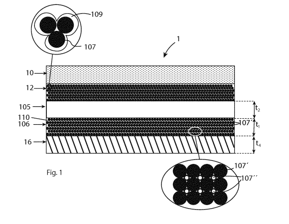
Figure 1 shows an example of a dye-sensitized solar cell unit 1. The solar
cell unit 1 comprises
a working electrode comprising a light-absorbing layer 10 and a porous first
conductive layer
12 for extracting photo-generated electrons from the light-absorbing layer 10.
Preferably, the
light-absorbing layer 10 is porous. The light-absorbing layer 10 is arranged
on top of the first
conductive layer 12. The solar cell unit 1 further comprises a porous
insulating layer 105 made
of an insulating material, wherein the first conductive layer 12 is arranged
on top of the porous
insulating layer 105. For example, the porous insulating layer 105 is a porous
substrate.
The solar cell unit 1 has a counter electrode comprising a porous catalytic
conductive layer
106 comprising porous conductive material 107' and catalytic particles 107"
distributed in the
porous conductive material 107' for improving the transfer of electrons to an
electrolyte 110
disposed in pores of the porous catalytic conductive layer 106. In one aspect,
the conductive
material 107' of the porous catalytic conductive layer 106 comprises
conductive particles 107'.
For example, the porous catalytic conductive layer 106 comprises a mixture of
conductive
particles 107' and catalytic particles 107", as shown in the enlarged figure
to the right in figure
CA 03099803 2020-11-09
WO 2020/015882 PCT/EP2019/061728
18
1. Preferably, the catalytic particles 107"are substantially evenly
distributed in the conductive
material 107' of the catalytic conductive layer 106.
The porous catalytic conductive layer 106 is arranged adjacent to the porous
insulating layer
.. 105 on an opposite side of the insulating layer compared to the first
conductive layer.
In one aspect, the counter electrode of the solar cell unit 1 comprises a
second conductive
layer 16 including a conductive material. The porous catalytic conductive
layer 106 is disposed
between the porous insulating layer 105 and the second conductive layer 16.
The catalytic
conductive layer 106 is in electrical contact with the second conductive layer
16. The second
conductive layer 16 is essentially non-catalytic. The first conductive layer
12, the catalytic
conductive layer 106, and the insulating layer 105 are porous to allow the
electrolyte to
penetrate through the layers to reach the light-absorbing layer 10. In one
aspect, the second
conductive layer is also porous. In an alternative embodiment, the second
conductive layer 16
.. can be omitted.
The solar cell unit 1 also comprises an ionic based electrolyte 110 for
transferring charges
between the counter electrode and the working electrode. For example, the
ionic based
electrolyte is a liquid or a gel. The ionic based electrolyte is located in
pores of the porous
layers, such as the porous first conductive layer 12, the catalytic conductive
layer 106, the
porous insulating layer 105, and the light-absorbing layer 10. The ionic based
electrolyte may
also be located in pores of the second conductive layer 16, if the second
conductive layer is
porous.
The conductive material in the porous catalytic conductive layer 106 is a part
of the counter
electrode. Consequently, since the catalytic conductive layer 106 and second
conductive layer
16 are in electrical contact, the effective distance between the light-
absorbing layer 10 and
the second conductive layer 16 is shorter and the resistive losses in the
conductive medium
are therefore reduced. Further, the catalytic particles 107" facilitating the
transfer of
.. electrons from the conductive material 107' in the porous catalytic
conductive layer to the
electrolyte 110.
In one aspect, the catalytic conductive layer 106 comprises a mixture of
conductive particles
107' and catalytic particles 107". The conductive particles are in electrical
contact with the
.. second conductive layer 16. Preferably, the conductive particles are non-
catalytic and exclude
catalytic material. The mixture of conductive particles and catalytic
particles will result in
efficient transfer of electrons from the catalytic conductive layer to the
electrolyte.
The conductive particles of the catalytic conductive layer include conductive
material and are
.. in electrical contact with the second conductive layer 16. The catalytic
particles are distributed
among the conductive particles. The conductive particles act as a holder for
the catalytic
CA 03099803 2020-11-09
WO 2020/015882 PCT/EP2019/061728
19
particles and keep them in place. The conductive particles may form a matrix
for housing the
catalytic particles and keeping them in place. For example, the matrix
comprises sintered
metal particles.
In one aspect, the catalytic particles are substantially evenly distributed
among the conductive
particles. By distributing the catalytic particles substantially evenly in the
catalytic conductive
layer, transfer of electrons from the conductive particles to the electrolyte
is improved. In one
aspect, the conductive particles are attached to each other, for example, by
sintering. The
conductive particle may form a matrix housing the catalytic particles. The
catalytic particles
are embedded in the matrix of conductive particles. For example, the catalytic
conductive
layer comprises sintered conductive particles, and catalytic particles are
disposed between
the conductive particles. The conductive particles act as a glue between
catalytic particles and
keep the catalytic particles in position between the conductive particles.
In one aspect, at least 80% of the catalytic particles 107" have a diameter
less than 50 nm.
Such small particles have a large surface/volume ratio and will provide an
efficient catalyzation
with a reduced volume of catalytic material. If the catalytic material is
platina, this will reduce
the cost for the catalytic material. In one aspect, at least 80% of the
conductive particles have
a diameter larger than 100 nm. Preferably, the size of conductive particles is
between 0.1 -15
M.
The conductive material of the first and second conductive layers 12, 16 can,
for example, be
metal, metal alloy, metal oxide, or other conductive materials, for example,
titanium, titanium
alloys, nickel, or nickel alloys. Suitably, the first and second conductive
layers 12, 16 comprise
titanium or an alloy thereof. For example, the conductive material of the
first and second
conductive layers is titanium. For example, the first conductive layer 12 may
comprise sintered
titanium particles in order to be porous. It is advantageous to use titanium
since it is highly
corrosion resistant, and ionic based electrolytes often are very corrosive.
The conductive material 107' in the catalytic conductive layer 106 can, for
example, be made
of metal, metal alloy, metal oxide, or other conductive materials, for
example, titanium,
titanium alloys, nickel, or nickel alloys, indium or indium oxide. The
catalytic particles 107"
are, for example, made of carbon-based materials such as graphene or graphite
or carbon
black or carbon nanotubes, platina or a combination thereof.
In one aspect, the catalytic particles 107" comprise carbon particles. Carbon
is inexpensive
and environmentally friendly. More preferably, the catalytic particles 107"
include platinized
carbon particles. Platina is a better catalyst than carbon, but it is
expensive. By using a
combination of platina and carbon, a good catalyst is achieved at a lower
cost. The catalytic
particles can be electrically conductive as well as catalytic. For example,
carbon is electrically
CA 03099803 2020-11-09
WO 2020/015882 PCT/EP2019/061728
conductive as well as catalytic. However, carbon is a poor conductor in
comparison to other
conductive material, such as titanium.
The electrical conductivity of the first and second conductive layer 12, 16
can be higher than
5 the electrical conductivity of the catalytic conductive layer 106. The
combination of a catalytic
conductive layer 106 with a mixture of conductive material and catalytic
particles, and a
second conductive layer 16 essentially without catalytic particles, will
result in efficient
transfer of electrons from the conductive particles 107' of the counter
electrode to the
electrolyte as well as high electrical conductivity of the counter electrode.
Preferably, the catalytic conductive layer comprises between 1 - 50 % by
weight of catalytic
particles. The % by weight of catalytic particles needed to achieve an
efficient transfer of
electrons from the conductive material to the electrolyte depends on the size
and shape of
the catalytic particles and the type of material in the catalytic particles
and the type of
conductive material. For example, the catalytic conductive layer may comprise
between 5 - 30
% by weight of catalytic particles. This range is, for example, suitable when
the conductive
particles consist of titanium and the catalytic particles consist of
platinized carbon. However,
as mentioned before, the % by weight of catalytic particles depends on the
size of the
particles.
For example, if the conductive material 107' in the catalytic conductive layer
106 is titanium,
the catalytic particles 107" comprise platinized carbon, and the size of the
catalytic particles
107" is less than the size of the conductive particles 107', the catalytic
conductive layer 106
may comprise between 5 - 30 % by weight of catalytic particles 107" to provide
an efficient
transfer of electrons to the electrolyte. For example, the catalytic
conductive layer comprises
between 50 and 90 % by weight of titanium, at least 5 % by weight of carbon,
and at least
0.001 % by weight of platina. Titanium has good mechanical strength and keeps
the platinized
carbon particles in their positions in the catalytic conductive layer. Thus,
carbon, platina and
titanium together provide a catalytic conducting layer with high mechanical
strength and a
high ability to transfer electrons to the electrolyte.
In one aspect, the thickness t1 of the catalytic conductive layer 106 is at
least 1 um, preferably
at least 5 um and most preferably at least 10 um. In one aspect, the thickness
t1 of the catalytic
conductive layer 106 is less than 100 um, and preferably less than 20 um. In
one aspect, the
thickness t2 of the porous insulating layer 105 is between 0.1 um and 20 um,
and preferably
between 0.5 um and 10 um. In one aspect, the thickness t4 of the second
conductive layer 16
is at least 1 um, preferably at least 10 um and preferably at least 20 um.
The first conductive layer 12 comprises an insulating oxide layer 109 formed
on the surface of
the conductive material, as shown in the enlarged figure to the left in figure
1. This oxide layer
109 is, for example, formed by oxidizing the conductive material of the first
conductive layer.
CA 03099803 2020-11-09
WO 2020/015882 PCT/EP2019/061728
21
The conductive material suitably comprises a metal or a metal alloy, for
example, titanium.
The surface of the conductive material is oxidized when it is exposed to air.
The oxide layer
109 can be formed by performing a heat treatment of the first conductive layer
in an oxidizing
environment so that the conductive material becomes oxidized. The insulating
oxide layer 109
provides an electrically insulating layer on the conductive material, which at
least partly
prevents transfer of electrons between the first conductive layer 12 and the
electrolyte
disposed in the pores of the first conductive layer 12.
In one aspect, the first conductive layer 12 comprises porous titanium, and a
titanium oxide
layer 109 formed on the surfaces of the porous titanium so that the oxide
layer 109 electrically
insulates the porous titanium of the first conductive layer and by that
prevents electrons from
leaking from the porous titanium in the first conductive layer to the
electrolyte in the pores
of the first conductive layer. Thus, the efficiency of the solar cell unit is
increased. For example,
the first conductive layer 12 comprises sintered titanium particles 107, and
the surfaces of the
sintered titanium particles 107 are covered by the titanium oxide layer 109,
as shown in the
enlarged figure to the left in figure 1. In one aspect, the thickness of the
titanium oxide layer
is larger than 5 nm, preferably larger than 10 nm, and more preferably larger
than 20 nm. In
one aspect, the thickness of the titanium oxide layer is between 10 and 200
nm, and preferably
between 20 ¨ 50 nm.
In particular, the combination of the insulating oxide layer 109 that prevents
electrons from
leaking from the first conductive layer to the liquid based electrolyte, and a
counter electrode
comprising a catalytic conductive layer 106 including catalytic particles 107"
distributed in a
porous conductive material 107, and a non-catalytic conductive layer 16 that
improves the
efficiency of the counter electrode, will result in an efficient solar cell
unit which is capable of
producing power in a wide range of different light conditions. The solar cell
unit works during
poor as well as excellent lighting conditions, for example, indoors in
artificial light, and
outdoors in the shadow and when exposed to strong sunlight.
In one aspect, the electrolyte is any of a iodide/triiodide electrolyte, a
copper complex-based
electrolyte, or a cobalt complex-based electrolyte, or a combination thereof.
In one aspect,
the electrolyte comprises iodide (I-) and triiodide (13-) and the content of
triiodide in the
conductive medium is between 1 mM and 20 mM. This embodiment makes it possible
to
achieve high power generation at low light intensities.
The insulating material of the porous insulating layer 105, is, for example,
an inorganic
material that is positioned between the first conductive layer 12 and the
catalytic conductive
layer 106, and insulates the first conductive layer 12 and the catalytic
conductive layer 106
from each other. The porous insulating layer 105 is, for example, made of
glass fibers, ceramic
microfibers, or materials derived by delaminating layered crystals such 2D
materials or
nanosheets.
CA 03099803 2020-11-09
WO 2020/015882 PCT/EP2019/061728
22
The solar cell unit 1 may comprise a porous substrate. The porous insulating
layer 105 may
comprise the whole substrate, as shown in figure 1, or only a part 114a of the
porous substrate
114 as shown in figure 2. According to one aspect, the porous substrate is a
sheet comprising
woven microfibers extending through the entire solar cell unit. For example,
the woven
microfibers are made of glass fibers.
Figure 2 shows an example of a dye-sensitized solar cell 1' comprising a
porous substrate 114
made of an insulating material. Like or corresponding parts in the figures 1
and 2 are indicated
with like numerals. The difference between the solar cells 1' and 1 is that
the porous catalytic
conductive layer 106' comprises a first part 114a of a porous substrate 114,
and the porous
insulating layer 105 comprises a second part 114b of the porous substrate 114.
The catalytic
conductive layer 106' comprises conductive particles 107' and catalytic
particles 107"
disposed in pores of the first part 114a of the porous substrate 114. The
conductive particles
107' of the catalytic conductive layer 106' form a conductive network 209
through the
insulating material of the part 114a of the porous substrate 114. The
conductive network 209
form one or more electrically conductive paths through the insulating material
of the first part
114a of porous substrate. The conductive particles 107' and the catalytic
particles 107" are
disposed in pores of the porous substrate 114. Preferably, the size of the
particles is less than
the size of the pores in the porous substrate to be able to be infiltrated
into the substrate
during production of the solar cell. The conductive network 209 provides an
extension of the
second conductive layer, which extends into the porous substrate 114. Due to
the conductive
network in the porous substrate, the distance between the counter electrode
and the light-
absorbing layer does no longer depend on the thickness of the porous
substrate. Thus, the
thickness of the insulating layer can be reduced, and by that the distance
between the counter
electrode and the light-absorbing layer can be reduced. Accordingly, the
resistive losses in the
electrolyte are reduced.
In the following an example of a method for manufacturing the solar cell unit
1 is briefly
described.
1) Preparing a first ink comprising conductive particles made of an
electrically conductive
material. The conductive particles are, for example, made of titanium hydride.
2) Preparing a second ink comprising a mixture of conductive particles and
catalytic
particles. The conductive particles are, for example, made of titanium hydride
(TiH2)
and the catalytic particles are, for example, platinized carbon particles.
3) Providing a porous insulating substrate, for example, a glass fabric.
4) Depositing conductive particles on one side of the porous insulating
substrate, for
example, by printing the first ink including the titanium hydride particles on
one side
of the porous insulating substrate.
5) The printed first ink is then allowed to dry in air,
CA 03099803 2020-11-09
WO 2020/015882 PCT/EP2019/061728
23
6) Depositing a mixture of catalytic particles and conductive particles on the
other side
of the porous insulating substrate, for example, by printing the second ink
including
the titanium hydride particles and platinized carbon particles on the other
side of the
porous insulating substrate.
7) The printed second ink is then allowed to dry in air,
8) Depositing conductive particles on top pf the catalytic conductive layer,
for example,
by printing the first ink including the titanium hydride particles on the
layer of mixture
of catalytic particles and conductive particles.
9) The printed first ink is then allowed to dry in air,
10) The porous insulating substrate with the printed layers is then vacuum
sintered, for
example, at 600 C for an hour. During the sintering process, the titanium
hydride is
transformed into titanium. Consequently, a first conductive layer including
sintered
titanium, a second conductive layer including sintered titanium, and a
catalytic
conductive layer including sintered titanium and platinized carbon particles
disposed
in pores between the sintered titanium are formed during the sintering
process.
11) The porous insulating substrate with the sintered conductive layers is
heated in air to
form titanium oxide on the surfaces of the sintered titanium of the first
conductive
layer.
12) A TiO2 based ink is printed on top of the first conductive layer and then
dried. The glass
fabric with the layers is heated, for example, to 600 C. Consequently, the
deposited
TiO2 layer is sintered.
13) The sintered TiO2 layer is dye-sensitized to form a light-absorbing layer,
14) An ionic electrolyte, for example, an iodide/triiodide (I-/13)- based
redox electrolyte, is
infiltrated in the porous layers.
15) The solar cell is sealed, for example, by a transparent encapsulation.
Alternatively, step 11 can be done simultaneously as sintering the TiO2 layer
in step 12.
The porous conductive layers can be deposited on the porous substrate by any
of screen
printing, slot die coating, spraying, or wet laying.
During the heat treatment of step 11, titanium oxide is also formed on the
catalytic conductive
layer. It could be assumed that the oxide layer on the catalytic conductive
layer would prevent
the electrons from being transferred between the conductive material and the
electrolyte
disposed in the pores of the catalytic conductive layer. Surprisingly, it has
been discovered
that the catalytic particles, for example, platinized carbon particles, enable
transfer of
electrons from the conductive material to the electrolyte despite the oxide
layer on the
.. conductive material of the catalytic conductive layer.
Figure 3 shows a view from above of an example of a photovoltaic charger 200.
The
photovoltaic charger 200 is specially adapted for powering portable electronic
devices that
can be used indoors as well as outdoors, such as earphones, laptops, tablets,
mobile phones,
and remote-control units. The photovoltaic charger 200 can also be used for
powering small
CA 03099803 2020-11-09
WO 2020/015882 PCT/EP2019/061728
24
electronic devices embedded in other physical devices, such as vehicles, and
home appliances,
called Internet of Things (loT).
The photovoltaic charger 200 comprises a solar cell unit 1, an encapsulation 5
enclosing the
solar cell unit 1, a first conductor 18, and a second conductor 20. The
photovoltaic charger
may further comprise connection elements (not shown) for connecting the
photovoltaic
charger 200 to the electronic device. The solar cell unit 200 is a monolithic
type DSC. The
monolithic type of DSC differs from the standard DSC in that it is created on
a single substrate,
with multiple layer disposed on the substrate.
The encapsulation comprises a plurality of penetrations in connection to the
first and second
conductors for connecting the photovoltaic device to the external device. In
other words,
there are penetrations in the encapsulation for accessing the power produced
by the
photovoltaic device. Some kind of wiring will be going through the
penetrations. For example,
the first and second conductors may extend out of the encapsulation through
the penetrations
to connect to wiring for powering the external device. Alternatively, wires
from the outside of
the encapsulation are going through the penetrations and electrically connect
to the first and
second conductors. The penetrations are tightly fit around the wiring passing
through the
encapsulation such that no gas or liquid can pass through penetrations. For
example, the
penetrations are openings in the encapsulation tightly fit around wiring
passing through the
encapsulation.
The encapsulation 5 comprises a plurality of penetrations 7a- b arranged in
connection to the
first conductor 18 and the second conductor 20 for connecting the photovoltaic
device 1 to
the external device and by that accessing the power produced by the
photovoltaic device. For
example, the penetrations are lead trough openings in the encapsulation. Some
kind of wiring
will be going through the openings. For example, the first and second
conductors 18, 20 may
extend out of the encapsulation through the penetrations 7a-b to connect to
wiring for
powering the external device, as shown in figure 3. Alternatively, wires from
the outside of
the encapsulation are going through the penetrations and are electrically
connected to the
first and second conductors. The penetrations are tightly fit around the
wiring such that no
gas or liquid can pass through them. The penetrations can be made by having
the wires or
conductors that should go through the holes in place when the encapsulation is
arranged on
the solar cell unit 1. The encapsulation consists of top sheet 5a and bottom
sheet 5b, which
are, for example, adhesive films that are put together over the solar cell
unit 1. Alternatively,
the top and bottom sheets are made of a flexible plastic material, and the
edges of the top
and bottom sheets are bonded to each other by melting the plastic material. If
the
wires/conductors are already in place between sheets before the bonding and
protrude at the
edges of the sheets, the penetrations will be created during the bonding.
Alternatively, the
penetrations comprise through holes in the encapsulation made after
encapsulation of the
solar cell unit. The through holes are sealed after the wires/conductors have
been arranged
CA 03099803 2020-11-09
WO 2020/015882 PCT/EP2019/061728
in the through holes. The locations of the penetrations will depend on the
position of the first
and second conductors. The number of penetrations can vary. There is at least
one
penetration for each of the first and second conductor. However, it is also
possible to have a
plurality of penetrations for each of the first and second conductors.
5 Figure 4 shows an enlargement of a cross section through a part of the
photovoltaic charger
200 shown in figure 3. The photovoltaic charger 200 comprises one solar cell
unit 1, or solar
cell unit 1', which is described in more details with reference to figures 1
and 2. For example,
the light-absorbing layer 10 comprises dyed TiO2. Conventional dyes known in
the art can be
used. A dye is chosen to give good efficiency of the solar cell, especially in
combination with a
10 copper-based conductive medium. The light-absorbing layer 10 is arranged
on top of the first
conductive layer 12. The porous light-absorbing layer 10 is a porous TiO2
layer deposited onto
the first conductive layer 12. The TiO2 layer comprises TiO2 particles dyed by
absorbing dye
molecules on the surface of the TiO2 particles. The light-absorbing layer 10
is positioned on a
top side of the solar cell unit 1. The top side should be facing the light to
allow the light to hit
15 the dye molecules of the working electrode.
The first conductive layer 12 is in direct electrical contact with the light-
absorbing layer 10. In
this example, the second conductive layer 16 is porous. However, in an
alternative
embodiment, the second conductive layer 16 does not have to be porous. For
example, the
20 second conductive layer can be made of a metal foil. In this example,
the porous insulating
layer 105 comprises at least a part of a porous substrate. The porous
substrate provides
electrical insulation between the first conductive layer 12 and the catalytic
conductive layer
106. The first conductive layer 12 and the catalytic conductive layer 106 are
separated
physically and electrically by the porous substrate. The porosity of the
porous substrate will
25 enable ionic transport through the insulating layer 105. The porosity of
the first conductive
layer 12 and the catalytic conductive layer 106 will enable ionic transport
between the counter
electrode and the working electrode.
The photovoltaic charger 200 contains only one single solar cell unit 1. At
least the first
conductive layer 12 and the porous substrate are continuously extending
through the entire
solar cell unit. The light-absorbing layer 10 and the second conductive layer
16 extend
continuously at least through a main part of solar cell unit.
The solar cell unit 1 is filled with an electrolyte for transferring charges
between the counter
electrode and the light-absorbing layer 10. The electrolyte is, for example, a
conventional III
-
3 electrolyte or a similar electrolyte, or a copper (Cu) based electrolyte, or
cobalt (Co) complex
based electrolyte. The electrolyte comprises ions, for example, iodide ions (I-
) and triiodide
ions (13-) or copper ions (Cu' and Cu). Sunlight is harvested by the dye,
producing photo-
excited electrons that are injected into the conduction band of the TiO2
particles and further
collected by the first conductive layer. At the same time, ions in the
electrolyte transport the
electrons from the second conductive layer to the light-absorbing layer 10.
The first conductor
CA 03099803 2020-11-09
WO 2020/015882 PCT/EP2019/061728
26
18 collects the electrons from the first conductive layer and the second
conductor provides
electrons to the second conductive layer such that the solar cell unit can
continuously produce
power from the incoming photons.
.. The electrolyte penetrates the pores of the light-absorbing layer 10, the
first conductive layer
12, the porous insulating layer 105, the second conductive layer 16 and the
catalytic
conductive layer 106 to allow the ions to be transferred between the light-
absorbing layer 10
and the second conductive layer 16 and by that transfer electrons from the
working electrode
to the light-absorbing layer.
There are many dyes that may be used and according to some aspects, the dye
comprises
triarylamine organic dye comprising any of, or a mixture of, dyes in the class
Donor-rt bridge-
Acceptor (D-ri-A) and in the class Donor-Acceptor-rt bridge-Acceptor (D-A-rt-
A). Such dyes give
good efficiency of the solar cell, especially in combination with a copper-
based conductive
medium. Of the first class photosensitizer are, for example, substituted
(dip he nyla mi nop he nyI)-thio phe ne-2-cya noacrylic acids
or substituted
(diphenylaminophenyl)cyclopenta-dithiophene-2-cyanoacrylic acids. Of the
second class are,
for example, substituted
(((diphenylaminophenyl)benzothia-diazolyI)-
cyclopentadithiophenyl)aryl/heteroary1-2-cyanoacrylic acids or (((diphenyl-
aminophenyI)-
cyclopentadithiophenyl)benzothiadiazolyl)aryl/heteroary1-2-cyano-acrylic
acids.
The first conductor 18 is electrically connected to the first conductive layer
12, and the second
conductor 20 is electrically connected to the second conductive layer 16. For
example, the
first and second conductors are made of metal to achieve high electrical
conductivity.
The encapsulation 5 comprises a top sheet 5a covering a top side of the solar
cell unit 1, and
a bottom sheet 5b covering a bottom side of the solar cell unit. The
encapsulation 5 encloses
the solar cell unit and the electrolyte and acts as liquid barrier for the
electrolyte and prevents
the electrolyte from leaking from the photovoltaic charger 200. The top sheet
5a is
transparent, or at least the part covering the active area of the solar cell
unit 1 is transparent.
The top sheet 5a on the top side of the solar cell unit covers the light-
absorbing layer 10 and
allows light to pass through. The top and bottom sheets 5a-b are, for example,
made of a
polymer material. A polymer material is robust and impact resistant, and
flexible. The top and
bottom sheets 5a-b are sealed at the edges in order to protect the solar cell
unit against the
surrounding atmosphere, and to prevent the evaporation or leakage of the
electrolyte from
the inside of the solar cell unit.
In one example, the porous substrate is a sheet comprising a fabric of woven
microfibers. A
microfiber is a fibre having a diameter less than 10 um and larger than 1 nm.
A fabric of woven
microfibers can be made very thin and mechanically very strong. The fabric of
woven
microfibers contains holes between the woven yarns. The porous substrate may
further
CA 03099803 2020-11-09
WO 2020/015882 PCT/EP2019/061728
27
comprise one or more layers of non-woven microfibers disposed on the woven
microfibers to
at least partly block the holes between the yarns. Further, the non-woven
layer provides a
smooth surface on the substrate, suitable for applying a smooth conductive
layer on the
substrate by printing. The substrate is, for example, made of glass, silica
(SiO2), alumina
(A1203), aluminosilicate or quartz. Suitably, the non-woven and woven
microfibers of the
porous substrate are made of glass fibres, which provides a robust and
flexible substrate. The
thickness of the fabric of woven microfibers is suitably between 4 um and 30
um, preferably
between 4 um and 20 um to provide the required mechanical strength at the same
time as it
is thin enough to enable a fast transport of ions between the counter
electrode and working
electrode.
In one aspect, light-absorbing layer 10, and the first conductive layer 12 are
non-transparent.
In this example, the upper surface of the solar cell unit 1 is homogeneously
black, as shown in
figure 3. The TiO2 of the light-absorbing layer is black. There are no
conductors extending
across the surface of the solar cell unit 1 as it is in the prior art solar
cell panels. This is because
the photovoltaic charger 200 only contains one single solar cell unit, and not
a plurality of
series connected solar cell units, as in the solar panels used in the prior
art photovoltaic
chargers.
The size of the solar cell unit, i.e. the length and width of the solar cell
unit, may vary
depending on which device it is adapted to charge. Accordingly, the active
area of the solar
cell unit may vary depending on the need of power for the device to charge.
There is no limit
to the possible shape and size of the solar cell unit. For example, the size
of the solar cell unit
may vary between 1x1 cm with an active area of 1 cm2 and 1x1 m with an active
area of 1 m2.
There is no upper limit to the length and width of the solar cell unit.
However, a solar cell unit
larger than 1x1 m can be bulky to handle during manufacturing of the solar
cell unit.
The photovoltaic charger 200 includes a single solar cell unit 1 and a boost
converter 22
electrically connected to the first and second conductors 18, 20. A boost
converter, also called
step-up converter or step-up regulator, is a DC-to-DC power converter that
steps up voltage
while stepping down current from its input to its output. The voltage produced
by the single
solar cell unit is too low to charge certain types or batteries, for example,
lithium batteries
that require at least 3.6 V. The boost converter is adapted to step up the
voltage from the
solar cell unit 1 while stepping down the current from the solar cell unit.
The required voltage
level is achieved by connecting a boost converter to the single solar cell
unit. Thus, it is possible
to provide a photovoltaic charger having only one single solar cell unit
capable to charge
batteries that require different voltage levels.
The photovoltaic charger 200 comprises connection elements 3, 4 for connecting
the
photovoltaic charger to a battery of the electronic device, which it is
charging. The boost
converter 22 comprises input terminals electrically connected to the first and
second
CA 03099803 2020-11-09
WO 2020/015882 PCT/EP2019/061728
28
conductors 18, 20 and output terminals electrically connected to the
connection elements 3,
4.
The level of the generated voltage depends on the ions in the electrolyte. For
example, if the
electrolyte contains copper ions, the solar cell unit generates a voltage of
about 1 V in an open
circuit when the light intensity received by the light-absorbing layer is 20
000 Lux, and if the
electrolyte contains iodide and triiodide ions, the solar cell unit generates
a voltage of about
0.65 V in an open circuit when the light intensity received by the light-
absorbing layer is 20 000
Lux. However, the solar cell unit 1 generates a voltage varying at most 0.4 V
in an open circuit
when the light intensity received by the light-absorbing layer is varying
between 200 and
000 Lux. The requirement on the voltage conversion of the boost converter
depends on
the voltage requirement of the rechargeable battery. Most types of
rechargeable batteries
used for electronic devices for consumer applications require a voltage
between 1 and 10 V.
The boost converter makes it possible to generate a stable voltage at a level
required by the
15 rechargeable battery. Preferably, the boost converter 22 is capable to
convert the output
voltage and current from the solar cell unit to a voltage level that lies
between 1 and 10 V.
Different boost converters can be used depending on the required output
voltage. Thus, the
photovoltaic charger is capable to charge batteries used for many types of
electronic devices,
such as lithium batteries (3.6V), NiCd and NiMH batteries (1.25 V).
From tests it has been shown that the solar cell unit is capable to produce a
current of at least
15 A/cm2 when the light intensity received by the light-absorbing layer is
200 Lux, and a
current of at least 1500 A/cm2 when the light intensity received by the light-
absorbing layer
is 20 000 Lux. Thus, the solar cell unit is capable to produce sufficient
power to charge
batteries of electronic devices in a wide range of light intensities.
According to some aspects, at least the first conductive layer 12 and the
porous substrate 114
are continuously extending through the entire solar cell unit 1. The light-
absorbing layer 10
and the second conductive layer 16 extend continuously at least through a main
part of the
solar cell unit.
Measurements of generated power per area for different light conditions have
been made on
an example of a photovoltaic charger of the invention including one single
solar cell unit 1. In
this example, the solar cell unit 1 has a size of 14.5 x 23.4 cm, and an
active area of 340 cm2.
The electrolyte of the solar cell unit 1 comprises iodide and triiodide ions,
and the first and
second conductive layers are made of titanium (Ti). The unloaded photovoltaic
charger is
exposed with light between 200 and 20 000 Lux (lumen per square meter), and
the output
voltage and output current from the photovoltaic charger is measured. The
results of the
measurements are shown in table 1 below. The total power generated is
determined based
on the measured current and voltage, and the generated power per area is
determined by
dividing the total power with the active area of the solar cell unit.
CA 03099803 2020-11-09
WO 2020/015882 PCT/EP2019/061728
29
Lux 1_c-12 I sc 4.1.12.,/ce-12, ',cc
2CC 6.2 72
c.C.0 8 44 521 77
ILCCO 37 90 54? 76
a: 179 565 79
266 =176 80
L4.5 79
6c6e. 2-1? 531 78
88C 13iL 75
73C ,-_ 69
Table 1 Measurements of generated power per active area, current per active
area, voltage
and fill factors (if) for light intensities between 200 ¨ 20 000 Lux for a
solar cell unit 1 having
an electrolyte comprising iodide (I-) and triiodide (13-) ions. The content of
triiodide is between
1 mM and 20 mM. Iodide works as ox and triiodide works as red.
The measurements of the performance of the solar cell unit 1 at different
light intensities
(intensities measured in Lux units) can be done by shining light on the solar
cell unit, and
simultaneously scanning an applied electrical voltage across the solar cell
unit to measure and
collect the current-voltage response of the solar cell. The measurements were
performed
using a warm ¨ white LED as light source.
The collected IV curve under illumination provides information about the open
circuit voltage,
short circuit current, fill factor, the power and the power conversion
efficiency. By collecting
IV curves at different light intensities, it is possible to gather information
on the light intensity
dependence of the open circuit voltage, short circuit current, fill factor the
power and the
power conversion efficiency, respectively.
The result from table 1 is from measurements on a sample of a solar cell unit
1. Measurements
on different solar cell units of this type may vary. For example, the
generated power per area
may from 5 uW/cm2 to 8 uW/cm2.
The light source used for shining light on the solar cell can vary depending
on the solar cell
application. For indoor applications it could be useful to use fluorescent
light bulbs or indoor
LED lighting. For solar cell applications that use outdoor light it could be
useful to shine light
on the solar cell using a solar simulator to generate artificial sunlight.
The light intensity of the light source can be measured in different ways, for
example, using a
lux meter or a spectroradiometer positioned at the same position as the solar
cell unit in
relation to the light source. In this case, the light intensity was measured
using a lux meter.
CA 03099803 2020-11-09
WO 2020/015882 PCT/EP2019/061728
Table 1 shows the determined power in microwatt per square centimetre (uW/cm2)
for
different light intensities measured in lux. As seen from the table, the solar
cell unit 1
generates 6.2 uW/cm2 when the light intensity received by the solar cell unit
1 is 200 Lux,
generates 208 uW/cm2 when the light intensity received by the solar cell unit
1 is 5000 Lux,
5 and generates 730 uW/cm2 when the light intensity received by the solar
cell unit 1 is 20 000
Lux. This shows that the photovoltaic charger is capable of producing more
than 5 uW/cm2,
and even more than 5.5 uW/cm2when the light intensity received by the light-
absorbing layer
is 200 Lux. This also shows that the photovoltaic charger is capable of
producing more than
700 uW/cm2 when the light intensity received by the light-absorbing layer is
20 000 Lux. Thus,
10 the solar cell unit 1 is at least capable of producing between 5,5 and
700 uW/cm2 when the
light intensity received by the light-absorbing layer is between 200 and 20
000 Lux. The power
produced by the photovoltaic charger increases substantially linear when the
light intensity
received by the light-absorbing layer increases from 200 to 20 000 Lux. Thus,
the photovoltaic
charger is capable of producing power in a wide range of different light
conditions.
Figure 5 shows a diagram of generated voltage (mV) for light intensities
between 200 and
000 Lux based on the measured values of table 1. As seen from the diagram and
table 1,
the solar cell unit 1 is capable to generate a voltage of 480 mV in an open
circuit when the
light intensity received by the solar cell unit 1 is 200 Lux. Further, the
photovoltaic charger 200
20 is capable to generate a voltage of 650 mV in an open circuit when the
light intensity received
by the solar cell unit 1 is 20 000 Lux. As seen from the diagram, the increase
of generated
voltage is largest between 200 and 3000 Lux. The generated voltage is
substantially linear
between 3000 and 20 000 Lux. As seen from the table 1, the difference in
generated voltage
between 200 and 20 000 Lux is only 167 mV. Thus, the solar cell unit 1
generates a voltage
varying less than 0.2 V in an open circuit when the light intensity received
by the light-
absorbing layer is varying between 200 and 20 000 Lux. Accordingly, the
difference in
generated voltage between 200 and 20 000 Lux is about 35%.
Figure 6 shows a diagram of generated current ( A/cm2) for light intensities
between 200 and
20 000 Lux based on the measured values of table 1. As seen from the figure,
the current
increase linearly.
Figure 7 shows a diagram of generated power per area (uW/cm2) for light
intensities between
200 and 20 000 Lux calculated based on the measured values of voltage and
current of table
1. As seen from the diagram, the measured power is substantially proportional
to the
incoming light intensity in the interval 200 ¨ 20 000 Lux.
Further measurements of generated power per area for different light
conditions have been
made on another example of a photovoltaic charger of the invention. In this
example, the
electrolyte of the solar cell unit 1 comprises copper ions (Cu + and Cu2+),
which is the only
difference between the photovoltaic chargers measured. The measurement
conditions were
CA 03099803 2020-11-09
WO 2020/015882 PCT/EP2019/061728
31
the same. The unloaded photovoltaic charger 200 is exposed with light between
200 and
20 000 Lux (lumen per square meter), and the output voltage and output current
from the
photovoltaic charger is measured. The result of the measurements is shown in
the table 2
below.
sc Voc (mV) tf
0 C 0 0
700 12.8 25 699 72,7
500 3S -67 762 74:3
85.4
2CCC 186 290 33; 771
56CC 737 3S 76.6
:CNC 1C2C 1490 95 75:1
2COCC 2020 296C 94372,
=JCOCC 7.1920 L=2.90 93-4 69.7_
4CC0C 372: 575C 938 67.6
3COCC, :1:!: 938 65.8
Table 2 Measurements of generated power per area, current per area, voltage
and fill factor
(ff) for light intensities between 200 ¨ 20 000 Lux for a solar cell unit 1
having an electrolyte
comprising copper ions; Cu+as red and Cu2+as ox.
As seen from the table 2, the solar cell unit 1 generates 12.8 uW/cm2 when the
light intensity
received by the solar cell unit 1 is 200 Lux, generates 498 uW/cm2 when the
light intensity
received by the solar cell unit 1 is 5000 Lux, and generates 2020 uW/cm2 when
the light
intensity received by the solar cell unit 1 is 20 000 Lux. This shows that
this photovoltaic
charger 200 is capable of producing more than 12 uW/cm2 when the light
intensity received
by the light-absorbing layer 10 is 200 Lux. This also shows that the
photovoltaic charger 200 is
capable of producing more than 2000 uW/cm2 when the light intensity received
by the light-
absorbing layer 10 is 20 000 Lux. The power produced by the photovoltaic
charger increases
substantially linear when the light intensity received by the light-absorbing
layer increases
from 200 to 20 000 Lux. Thus, the photovoltaic charger 200 is capable of
producing power in
a wide range of different light conditions.
Figure 8 shows a diagram of generated voltage (mV) for light intensities
between 200 and
50 000 Lux based on the measured values of table 2. As seen from the diagram
and table 2,
the solar cell unit 1 is capable of generating a voltage of 699 mV in an open
circuit when the
light intensity received by the solar cell unit 1 is 200 Lux. Further, the
photovoltaic charger 200
is capable to generate a voltage of 943 mV in an open circuit when the light
intensity received
by the solar cell unit 1 is 20 000 Lux. As seen from the diagram, the
generated voltage is
substantially linear between 3000 and 50 000 Lux. As seen from the table 2,
the difference in
generated voltage between 200 and 20 000 Lux is only 244 mV. Accordingly, the
difference in
CA 03099803 2020-11-09
WO 2020/015882 PCT/EP2019/061728
32
generated voltage between 200 and 20 000 Lux is about 35%. The difference in
generated
voltage between 200 and 50 000 Lux is only 259 mV. Thus, the solar cell unit 1
generates a
voltage varying less than 300 mV in an open circuit when the light intensity
received by the
light-absorbing layer is varying between 200 and 50 000 Lux. Accordingly, the
difference in
generated voltage between 200 and 50 000 Lux is about 37%.
Figure 9 shows a diagram of generated current ( A/cm2) for light intensities
between 200 and
50 000 Lux based on the measured values of table 2. As seen from the figure,
the current
increases linearly.
Figure 10 shows a diagram of generated power per area (uW/cm2) for light
intensities
between 200 and 50 000 Lux calculated based on the measured values of voltage
and current
of table 1. As seen from the diagram, the measured power is substantially
proportional to the
incoming light intensity in the interval 200 ¨ 20 000 Lux.
.. The present invention is not limited to the embodiments disclosed but may
be varied and
modified within the scope of the following claims. For example, the second
conductive layer
16 can be omitted. Omitting the second conductive layer may reduce the range
of different
light conditions in which the solar cell unit can produce enough power for
powering a device.
However, in some applications the light conditions do no vary that much and a
solar cell unit
capable to produce power in a smaller range is enough.