Note: Descriptions are shown in the official language in which they were submitted.
1
Description
Fixed -Admittance Modeling and Real-Time Simulation Method for Power
Electronic Converter
Technical Field
The invention relates to the technical field of power systems, and
specifically relates to a
constant-admittance modeling and real-time simulation method for a power
electronic converter.
Background Art
Electromagnetic transient simulation is an important part of power system
simulation. The basic
theory and method of power system electromagnetic transient simulation was
proposed by H. W.
Dommel, Canada in the late 1960s. For applications of different types,
electromagnetic transient
simulation can be divided into off-line simulation and real-time simulation.
In general, off-line
simulation tools take much longer time for computation than duration time of
transient phenomena
under research. When facing application scenarios having strict requirements
on time, a real-time
simulator ensures accurate synchronization of the internal clock of the
simulator and the
real-world clock through cooperation of software and hardware platforms, and
can provide a test
environment that closely simulates an actual field for various power system
protection and control
devices.
As more and more power electronic devices are introduced into power systems,
the
high-frequency discrete characteristics of power electronic switches offer
great challenges for
modeling and real-time simulation of power electronic devices. At present, in
electromagnetic
transient simulation, modeling methods generally used for power electronic
switches can be
divided into the following two types:
1) two-value resistor modeling, namely using a small resistor as an equivalent
of a switch when
the switch is turned on, and using a large resistor as an equivalent of the
switch when the switch is
turned off; and
2) inductor/capacitor equivalent based constant-admittance modeling, namely
using a small
inductor as an equivalent of a switch when the switch is turned on, and using
a small capacitor as
an equivalent of the switch when the switch is turned off;
when binary resistor modeling is used, an abrupt change in the admittance of a
switch branch is
caused when the state of the switch changes, and the admittance matrix needs
to be reformed
every time a switching operation occurs, so that the efficiency is low, the
real-time requirement
cannot be met, and binary resistor modeling is often applied to off-line
electromagnetic transient
Date Recue/Date Received 2021-05-04
2
simulation tools, such as PSCAD/EMTDC, Simulink/SimPowerSystem, EMTP series
simulation
software and the like; and
in inductor/capacitor equivalent based constant-admittance modeling,
equivalent admittances of
small inductors and small capacitors can be equalized through reasonable
parameter setting to
prevent changes of the admittance matrix caused by switching operations, so
that the simulation
efficiency is greatly improved, and inductor/capacitor equivalent based
constant-admittance
modeling is often applied to Small time-step model libraries of RTDS (Real-
Time Digital Simulator).
However, due to limitation of physical characteristics of inductors and
capacitors,
constant-admittance modeling has an obvious transient error after a switching
operation occurs,
and the power loss of a converter In the real-time simulation is much larger
than the actual
situation, which greatly influences the precision of simulation, and this
phenomenon is called
virtual power loss problem.
At present, no description or report of technology similar to the present
invention has been found,
and no similar information has been collected at home or abroad.
Summary of the Invention
To overcome the defects in existing power electronic converter modeling
methods, an object of
the invention is to provide a constant-admittance modeling and real-time
simulation method
specifically used for a power electronic converter, and the method prevents
changes of an
admittance matrix caused by switching operations, and also solves the problem
of virtual power
loss of conventional modeling simulation methods in real-time simulation of
power electronic
converters, thereby greatly improving the precision of simulation.
The present invention is realized by the following technical scheme.
A constant-admittance modeling and real-time simulation method for a power
electronic converter
comprises the following steps of:
Si, numbering each branch and each node in the power electronic converter and
in a circuit where
the power electronic converter resides, wherein a grounding node is numbered
as 0;
S2, replacing each of resistor branches, inductor branches, capacitor branches
and switch branches
with a respective equivalent model formed by an equivalent admittance and a
history current
source which are connected in parallel; replacing an independent voltage
source branch with an
equivalent model foimed by an equivalent admittance and an equivalent current
source which are
connected in parallel, and calculating the equivalent admittance of the
equivalent model of each
branch, wherein the equivalent admittance of the equivalent model of each
switch branch is
constant in both an on state and an off state;
S3, calculating a node admittance matrix of a circuit to be simulated
according to the equivalent
Date Recue/Date Received 2021-05-04
3
admittance of each branch;
S4, if a current simulation time t is a simulation initial time, taking
magnitudes of the historical
current sources of the resistor branches, the inductor branches, the capacitor
branches and the
switch branches as zero, and separately calculating an equivalent current of
the independent
voltage source branch; and if the current simulation time t is not the
simulation initial time,
calculating magnitudes of the historical current sources of the resistor
branches, the inductor
branches, the capacitor branches and the switch branches at the current
simulation time according
to branch voltages and branch currents of the resistor branches, the inductor
branches, the
capacitor branches and the switch branches at a previous simulation time, and
separately
calculating the equivalent current of the independent voltage source branch;
S5, calculating an injection current flowing into each node according to the
magnitudes of the
historical current sources and the magnitude of the equivalent current source
at the current
simulation time;
S6, calculating a voltage of each node according to the injection current
flowing into each node in
combination with the node admittance matrix;
S7, calculating the branch voltage and the branch current of each branch
according to the voltage
of each node in combination with the equivalent admittance of each branch; and
S8, if a final simulation time is not reached, returning to S4, and entering a
next simulation time
t + At ; otherwise, ending.
Preferably, the equivalent admittance of each branch is calculated according
to the following
formulae:
1
Yb R =
the equivalent admittance of each resistor branch is: R;
wherein, R is a resistance of the
resistor branch;
At
Yb L
the equivalent admittance of each inductor branch is: L;
wherein, L is an inductance
of the inductor branch, and At is a time step of real-time simulation;
Yb C = ¨
the equivalent admittance of each capacitor branch is: At;
wherein, C is a capacitance
of the capacitor branch;
v
/h
the equivalent admittance of each switch branch is: L" ;
wherein, Cdc is a
capacitance of a direct-current side of the power electronic converter, and
Lac is an inductance
Date Recue/Date Received 2021-05-04
4
of an alternating-current side of the power electronic converter; and
1
Y = ¨
b _Vs R R
the equivalent admittance of the independent voltage source branch is: ;
wherein
is an internal resistance of the independent voltage source branch.
When the power electronic converter is a three-level converter, historical
currents and the
equivalent current are calculated according to the following formulae:
I h R =0
the historical current of each resistor branch is:
I h L (t) = L w
(t ¨ At) ; herein, i (t ¨ At)
the historical current of each inductor branch is: is
the branch current of the inductor branch at the previous simulation time;
I h C (t) = ¨Yb (t ¨ At)
the historical current of each capacitor branch is: ;
wherein,
uc (t ¨At)
is the branch voltage of the capacitor branch at the previous simulation time,
and
Yb-c is the equivalent admittance of the capacitor branch;
in the on state, the historical current of each switch branch is:
h (t) = -5.04Y/, õvu (t (t ¨At)
; and in the off state, the historical current of
(t) = Ybsw (t ¨ (t ¨
At); wherein, u (t ¨ At)
each switch branch is: h
is the branch voltage of the switch branch at the previous simulation time,
lSV(t ¨ At) is the
branch current of the switch branch at the previous simulation time, and b -
'"4' is the equivalent
admittance of the switch branch;
ii' (t)
'v. (t) ¨ ___________________________________________________________
the equivalent current source of the independent voltage source branch is
Vs
wherein, (t) is
an internal electric potential of the independent voltage source branch, and
Rs is the internal resistance of the independent voltage source branch; and
when the power electronic converter is a two-level converter, historical
currents and the equivalent
current are calculated according to the following folinulae:
I h R =0
the historical current of each resistor branch is:
I h L (t) = L (t At ) ; wherein, i (t ¨ At)
the historical current of each inductor branch is: is
the branch current of the inductor branch at the previous simulation time;
Date Recue/Date Received 2021-05-04
I h C (t) = ¨Yb cti (t ¨ At)
the historical current of each capacitor branch is: ;
wherein,
uc (t ¨ At)
is the branch voltage of the capacitor branch at the previous simulation time,
and
b-c is the equivalent admittance of the capacitor branch;
in the on state, the historical current of each switch branch is:
h (t) = (-1 11)17 swt sw (t ¨ At) ¨ ,sw (t ¨ At)
; and
in the off state, the historical current of each switch branch is:
h sw (t) = Y
or,
in the on state, the historical current of each switch branch is:
sw (t) = (-1 ¨ -5,)n õvu (t_Ao_c (t_At)
; and
in the off state, the historical current of each switch branch is:
wherein, it' (t ¨ At)
is the branch voltage of the switch branch at the previous simulation time,
isw (t ¨ At)
is the branch current of the switch branch at the previous simulation time,
and
is the equivalent admittance of the switch branch; and
Vs (t)
is v.(t) ¨ ______________________________________________________
the equivalent current source of the independent voltage source branch is
(t) i wherein, s an
internal electric potential of the independent voltage source branch, and
Rs is the internal resistance of the independent voltage source branch.
Compared with the prior art, the method provided by the present invention has
the following
technical effects:
(1) According to the invention, in the power electronic converter, the
equivalent admittance of the
equivalent model of each switch branch is constant in both the on state and
the off state, so that the
operation of refolining an admittance matrix due to a change in the switch
state in a simulation
process is prevented, and therefore the simulation efficiency is guaranteed
and real-time
requirement can be met.
(2) Compared with conventional inductor/capacitor equivalent based methods,
the method
provided by the present invention can provide a real-time simulation wavefolin
closer to an ideal
Date Recue/Date Received 2021-05-04
6
switch waveform, and the precision of real-time simulation of the power
electronic converter is
greatly improved. A converter composed of ideal switches has no virtual power
loss, while in
conventional inductor/capacitor equivalent based methods, the virtual power
loss of the power
electronic converter increases along with the increase of switching frequency,
as shown in Fig. 3,
to an extent of up to 60% or more at 100 kHz, and is greatly not matched with
the actual situation.
By using the method provided by the present invention, the virtual power loss
of the power
electronic converter substantially does not change along with the switching
frequency and is
always maintained at a level close to zero, and the power electronic converter
is closer to a
converter composed of ideal switches.
According to an aspect of the invention there is provided a computer-
implemented method for
constant-admittance modeling and real-time simulation of a power electronic
converter, which is
performed on a computer system including a field programmable gate array
(FPGA) and a
computing device communicatively coupled thereto, the method being
characterized by
comprising the following steps of:
Si, using the computer system, numbering each branch and each node in the
power electronic
converter and in a circuit where the power electronic converter resides,
wherein a grounding node
is numbered as 0;
S2, using the computer system, replacing each of resistor branches, inductor
branches, capacitor
branches, and switch branches in the power electronic converter with a
respective equivalent
model formed by an equivalent admittance and a historical current source which
are connected in
parallel; replacing an independent voltage source branch with an equivalent
model formed by an
equivalent admittance and an equivalent current source which are connected in
parallel, and
calculating the equivalent admittance of the equivalent model of each branch,
wherein the
equivalent admittance of the equivalent model of each switch branch is
constant in both an on
state and an off state;
S3, using the computer system, calculating a node admittance matrix of a
circuit to be simulated
according to the equivalent admittance of each branch;
S4, using the computer system, if a current simulation time t is a simulation
initial time, taking
magnitudes of the historical current sources of the resistor branches, the
inductor branches, the
capacitor branches and the switch branches as zero, and separately calculating
an equivalent
current of the independent voltage source branch; and
if the current simulation time t is not the simulation initial time,
calculating magnitudes of the
historical current sources of the resistor branches, the inductor branches,
the capacitor branches
and the switch branches at the current simulation time according to branch
voltages and branch
Date Recue/Date Received 2021-05-04
6a
currents of the resistor branches, the inductor branches, the capacitor
branches and the switch
branches at a previous simulation time, and separately calculating the
equivalent current of the
independent voltage source branch;
S5, using the computer system, calculating an injection current flowing into
each node according
to the magnitudes of the historical current sources and the magnitude of the
equivalent current
source at the current simulation time;
S6, using the computer system, calculating a voltage of each node according to
the injection
current flowing into each node in combination with the node admittance matrix;
S7, using the computer system, calculating the branch voltage and the branch
current of each
branch according to the voltage of each node in combination with the
equivalent admittance of the
equivalent model of each branch; and
S8, if a final simulation time is not reached, returning to S4 and entering a
next simulation time
t + At ; otherwise, ending.
Brief Description of the Drawings
Other features, objects and advantages of the present invention will become
apparent by taking the
following detailed description of non-limiting embodiments with reference to
the accompanying
drawings in which:
Fig. 1 shows a schematic diagram of an equivalent model of resistor branches,
inductor branches,
capacitor branches and switch branches according to the present invention;
Fig. 2 shows a current wavefoim comparison of a constant-admittance modeling
and real-time
simulation method for a three-level converter according to Embodiment 1 of the
present invention;
Fig. 3 shows a voltage waveform comparison of the constant-admittance modeling
and real-time
simulation method for the three-level converter according to Embodiment 1 of
the present
invention;
Fig. 4 shows virtual power loss rates under different converter switching
frequencies of the
constant-admittance modeling and real-time simulation method for the three-
level converter
according to Embodiment 1 of the present invention;
Fig. 5 shows a circuit diagram of the constant-admittance modeling and real-
time simulation
method for the three-level converter according to Embodiment 1 of the present
invention; wherein,
(a) is a circuit diagram of a single-phase three-level converter, (b) is an
circuit diagram of a
general three-level converter equivalent circuit, and (c) is circuit diagram
of a three-level
converter constant-admittance equivalent model;
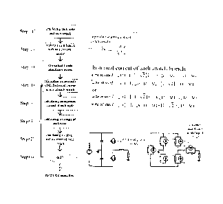
Fig. 6 shows a flow chart of the constant-admittance modeling and real-time
simulation method
for the three-level converter according to Embodiment 1 of the present
invention;
Fig. 7 shows a current wavefoim comparison of a constant-admittance modeling
and real-time
Date Recue/Date Received 2021-05-04
6b
simulation method for a two-level converter according to Embodiment 2 of the
present invention;
Fig. 8 shows a simple circuit including a single-phase two-level bridge
converter; and
Fig. 9 shows a flow chart of the constant-admittance modeling and real-time
simulation method
Date Recue/Date Received 2021-05-04
7
for the two-level bridge converter according to Embodiment 2 of the present
invention.
Detailed Description of the Invention
Embodiments of the present invention are described in detail below: the
embodiments are
implemented based on the technical scheme of the invention, and detailed
implementations and
specific operation processes are provided. It should be noted that several
variations and
modifications may be made by those skilled in the art without departing from
the spirit of the
invention and shall all fall within the scope of the invention.
Embodiment 1: A constant-admittance modeling and real-time simulation method
for a three-level
converter comprises the following steps that:
Step (1), each branch and each node in the three-level converter and in a
circuit where the
three-level converter resides are numbered, wherein a grounding node is
numbered as 0;
Step (2), each of resistor branches, inductor branches, capacitor branches and
switch branches is
replaced with a respective equivalent model founed by an equivalent admittance
and a historical
current source which are connected in parallel, and an independent voltage
source branch is
replaced with an equivalent model founed by an equivalent admittance and an
equivalent current
source which are connected in parallel; wherein, the equivalent admittance of
each branch is
calculated according to the following formulae:
1
Y = ¨
b R R
the equivalent admittance of each resistor branch is
wherein, R is an resistance of the resistor branch;
At
Yb L
the equivalent admittance of each inductor branch is
wherein, L is an inductance of the inductor branch, and At is a time step of
real-time
simulation;
Yb C ¨At
the equivalent admittance of each capacitor branch is
wherein, C is a capacitance of the capacitor branch;
the switch branches, namely the switch branches in the three-level converter,
each is replaced with
an equivalent model founed by an equivalent admittance and a historical
current source which are
connected in parallel, and the equivalent admittance of each switch branch is
constant in both an
on state and an off state, namely the equivalent admittance of each switch
branch is
Date Recue/Date Received 2021-05-04
8
v = Cde
b
ac
wherein, dc is a capacitance of a direct-current side of the three-level
converter, and Lac is an
inductance of an alternating-current side of the three-level converter; and
1
Y = ¨
b Vs R
the equivalent admittance of the independent voltage source branch is
wherein, is the internal resistance of the independent voltage source
branch;
Step (3), a node admittance matrix of a circuit to be simulated is calculated
according to the
equivalent admittance of each branch;
Step (4), if a current simulation time t is a simulation initial time,
magnitudes of the historical
current sources of the resistor branches, the inductor branches, the capacitor
branches and the
switch branches are taken as zero, and an equivalent current of the
independent voltage source
branch is separately calculated, and if the current simulation time t is not
the simulation initial
time, magnitudes of the historical current sources of the resistor branches,
the inductor branches,
the capacitor branches and the switch branches at the current simulation time
are calculated
according to branch voltages and branch currents of the resistor branches, the
inductor branches,
the capacitor branches and the switch branches at a previous simulation time,
and an equivalent
current of the independent voltage source branch is separately calculated;
wherein, a historical
current of each branch and the equivalent current are calculated according to
the following
foi __ inulae:
the historical current of each resistor branch is Ih -R = 0 =
I h L (t) = L (t ¨ At)
the historical current of each inductor branch is
wherein, i (t ¨ At)
is the branch current of the inductor branch at the previous simulation time;
I h C (t) = ¨Y, cuc. (t ¨ At)
the historical current of each capacitor branch is
wherein, uc ( t ¨ At)
is the branch voltage of the capacitor branch at the previous simulation
time, and h -C is the equivalent admittance of the capacitor branch;
in the on state, the historical current of each switch branch is
h (t) = -5 .04Yb õvu (t ¨ At) ¨ (t ¨ At)
and in the off state, the historical current of each switch branch is
Date Recue/Date Received 2021-05-04
9
hsw (t) = Y b õyid (t ¨ At) ¨ 0.39ç (t ¨ At)
wherein, it' (t ¨ At)
is the branch voltage of the switch branch at the previous simulation time,
(t ¨ At)
is the branch current of the switch branch at the previous simulation time,
and
is the equivalent admittance of the switch branch;
Vs (t)
is vs (t) ¨ _____________________________________________________
the equivalent current source of the independent voltage source branch is
wherein, vs (t)s an internal electric potential of the independent voltage
source branch, and
Rs is the internal resistance of the independent voltage source branch;
Step (5), an injection current flowing into each node is calculated according
to the magnitudes of
the historical current sources and the magnitude of the equivalent current
source at the current
simulation time;
Step (6), a voltage of each node is calculated according to the injection
current flowing into each
node in combination with the node admittance matrix;
Step (7), the branch voltage and the branch current of each branch are
calculated according to the
voltage of each node in combination with the equivalent admittance of the
equivalent model of
each branch; and
Step (8), if a final simulation time is not reached, the process returns to
Step (4) and enters a next
simulation time t + At; otherwise, the process is ended.
In order to facilitate understanding, the above embodiment of the present
invention will be further
explained below with reference to a simple circuit of a single-phase three-
level converter as shown
in Fig. 5 as a specific application example, but the scope of the present
invention should not be
limited thereby.
In the specific realization of real-time simulation of the three-level
converter, the following
hardware platfoims are adopted in this specific application example: a PXIe-
8135 (a PXIe
controller) and a PXIe-7975R (an FPGA module) of the National Instruments (NI)
Corporation are
separately installed in a PXIe chassis, the PXIe controller is mainly
responsible for simulation of a
converter control system, the FPGA module is mainly responsible for simulation
of circuit parts of
the three-level converter, and communication between the PXIe controller and
the FPGA module
is achieved through a PXIe bus. In addition, the PXIe controller can also
communicate with an
upper computer through Ethernet such that real-time simulation wavefollns are
displayed on the
upper computer, and the FPGA module can be connected with an external
controller and an
oscilloscope through I/O ports to perfoun hardware-in-loop simulation.
Date Recue/Date Received 2021-05-04
Programs in the upper computer, the PXIe controller and the FPGA module are
all programmed in
a LabVIEW development environment of the National Instruments (NI)
Corporation. Through
L abview programming, the programs in the host computer perform functions of
communicating
with the PXIe controller, displaying the simulation waveforms, etc.; and the
programs in the PXIe
controller perform functions of communicating with the upper computer, reading
data from and
writing data into the FPGA module, simulating the control system of the
converter, etc. The
above-described programs do not fall within the scope of the present
invention, and relevant
program examples are available on the official website of the National
Instruments (NI)
Corporation, therefore the programs will not be described in detail here.
However, the FPGA
module is the specific implementation carrier of the invention and is
programmed through
L abview, referring to Fig. 5 which is a circuit diagram of a constant-
admittance modeling and
real-time simulation method for a single-phase three-level converter according
to this specific
application example.
The constant-admittance modeling and real-time simulation method for the
single-phase
three-level converter according to the specific application example comprises
the following steps
that:
(1) each branch and each node in the three-level converter and in a circuit
where the three-level
converter resides are numbered, as shown in Fig. 5b;
(2) each of resistor branches, inductor branches, capacitor branches and
switch branches is
replaced with a respective equivalent model (as shown in Fig. 1) follued by an
equivalent
admittance and a historical current source which are connected in parallel,
and an independent
voltage source branch is replaced with an equivalent model foimed by an
equivalent admittance
and an equivalent current source which are connected in parallel, wherein a
simulation step is
taken as 1ps , and the equivalent admittance of each branch is as follows:
1 , õ
b Vs
branch 1 (independent voltage source branch) 0.1
¨ 3
branch 2 (capacitor branch)
b _Cdcl = 2e __ = 2000Q-1
le ¨ 6
¨ 3
branch 3 (capacitor branch) Y, = 2e _____ = 2000Q-1
_Cdc 2
le ¨ 6
branch 4 (switch branch) Yb = 2e ¨ 3 = 0.2 1-2-1
50e ¨ 3
¨ 3
branch 5 (switch branch) Yb 2e ________ = 0.2 Q-1
2
50e ¨ 3
Date Recue/Date Received 2021-05-04
11
2e ¨ 3
branch 6 (switch branch) sm,3 = = 0.2 Q-1
50e ¨ 3
branch 7 (inductor branch) Y L le -6 ¨ ¨ 2e 4 Q-1
50e ¨ 3
b R
branch 8 (resistor branch) 10
and the calculated value of the equivalent admittance of each branch is also
marked in Fig. St);
(3) a node admittance matrix Yn of a circuit to be simulated is calculated
according to the
equivalent admittance of each branch
2010.2 ¨10 ¨0.2 0
¨10 2010.2 ¨0.2 0
Yn
¨0.2 ¨0.2 0.6002 ¨2e-4
0 0 ¨2e-4 0.1002_
(4.0) if a current simulation time t = 0 its is a simulation initial time,
magnitudes of the
historical current sources of the resistor branches, the inductor branches,
the capacitor branches
and the switch branches are taken as zero, and an equivalent current of the
independent voltage
source branch is separately calculated, i.e.:
/ =50 =7500 A
branch 1 (independent voltage source branch) s-vs 0.1
branch 2 (capacitor branch) I h _cdel = 0 A
branch 3 (capacitor branch) I h_õc2 = 0 A
branch 4 (turned-off switch branch) /h sw1 = 0 A
branch 5 (turned-off switch branch) Ih_sw2 = 0 A
branch 6 (turned-on switch branch) Ih 3 = 0 A
branch 7 (inductor branch)
h L = 0 A
/ =OA
branch 8 (resistor branch) h R
(5.0) an injection current flowing into each node is calculated according to
the magnitudes of the
historical current sources and the magnitude of the equivalent current source
at the current
simulation time (an inflow current is positive and an outflow current is
negative):
Date Recue/Date Received 2021-05-04
12
injection current of node 1 1 = 7500 A
injection current of node 2 /n2 = ¨7500 A
injection current of node 3 In3 = 0 A
injection current of node 4 /n4 = OA
(6.0) a voltage of each node is calculated according to a node voltage
equation Icy, = I. with
the injection current, which has been given, flowing into each node in
combination with the node
admittance matrix:
V =3.7125V
voltage of node 1 "1
voltage of node 2 Vn2 = ¨3.7125 V
voltage of node 3 Vn3 = 0 V
voltage of node 4 Vn4 = 0 V
(7.0) a branch voltage and a branch current of each branch are calculated
according to the voltage
of each node in combination with the equivalent admittance of each branch:
V = 7.4250V / = 7.4257e3A
branch 1 (independent voltage source branch) b_vB b Vs
branch 2 (capacitor branch) Vo,. _Cdcl = 3.7125 V, I b = 7.4250e3 A _Cdcl
branch 3 (capacitor branch) V, _cde2 = 3.7125 V, _cdc2 = 7.4250e3 A
branch 4 (switch branch) T' = 3.7125 V, 'b1 = 0.7425 A
b _swl
branch 5 (switch branch) V2 = 3.7125 V,b s,4,2 = 0.7425 A
b _sw
branch 6 (switch branch) V = 0 V,b s,4,3 = OA
b _sw3
branch 7 (inductor branch) ''La = 0 V,b Lac = 0 A
b
branch 8 (resistor branch) Võ = 0 V, /õ = OA
t = 0 ps
(8.0) if the current simulation time does not
reach a final simulation time, the process
returns to the step (4.0) and enters a next simulation time t = 1,us
the process enters the next simulation time = 1
Date Recue/Date Received 2021-05-04
13
(4.1) if the current simulation time t = 1 ,t/S is not the simulation initial
time, a magnitude of the
historical current source of each branch at the current simulation time is
calculated according to
the branch voltage and the branch current of each branch at the previous
simulation time, wherein
a historical current of each branch and an equivalent current are calculated
according to the
following formulae:
750 õõõ A
/ = ¨= UU
s vs
branch 1 (independent voltage source branch) 0.1
branch 2 (capacitor branch)
h _Cdel = -7.4250e3A
branch 3 (capacitor branch) I h_cdc2 = -7.4250e3 A
branch 4 (turned-off switch branch) 'h1 = -0.4529 A
branch 5 (turned-off switch branch)
h sw2 ¨ -0.4529 A
branch 6 (turned-on switch branch)h 3 = 0 A
branch 7 (inductor branch)
h L = 0 A
Ih R =OA
branch 8 (resistor branch)
(5.1) an injection current flowing into each node is calculated according to
the magnitudes of the
historical current sources and the magnitude of the equivalent current source
at the current
simulation time;
injection current of node 1 In1 =1.4925e4 A
injection current of node 2 /n2 = ¨1.4925e4 A
injection current of node 3 I3 = 0 A
injection current of node 4 In4 = OA
(6.1) a voltage of each node is calculated according to the injection current
flowing into each node
in combination with the node admittance matrix;
V = 7.3881V
voltage of node 1 ni
voltage of node 2 Vn2 = ¨7.3881V
voltage of node 3 Vn3 = 3.6998e-16 V
Date Recue/Date Received 2021-05-04
14
voltage of node 4 V" = 7.3847e-19 V
(7.1) the branch voltage and the branch current of each branch are calculated
according to the
voltage of each node in combination with the equivalent admittance of each
branch;
V = 14.7762 V / = 7.3522e3 A
b _V b Vs
branch 1 (independent voltage source branch) s
branch 2 (capacitor branch) = 7.3512e3 A
_Cdcl = 7.3881V, -11, _Cdcl
branch 3 (capacitor branch) = 7.3512e3 A
_ c Cd 2 = 7.3881V, b _Cdc2
branch 4 (switch branch) T7, swi = 7.3881 V, swi= 1.0247 A
branch 5 (switch branch) J22 = 7.3881V, Ib sm, 2 = 1.0247 A
branch 6 (switch branch) V = 3.6998e-16 V, lb sw3 = 7.3995e-17A
b _sw3
branch 7 (inductor branch) Vb _Lac = 3.6924e-16 V, lb Lac = 7.3847e-20A
branch 8 (resistor branch) VbR = 7.3847e-19 V, Iõ = 7.3847e-20A
(8.1) if the current simulation time t = 1 ps does not reach a final
simulation time, the process
returns to the step (4.1) and enters a next simulation time t = 2 is
the process enters the next simulation time t = 2 is :
(4.2) if the current simulation time t = 2 ps is not the simulation initial
time, the magnitude of
the historical current source of each branch and the equivalent current at the
current simulation
time are calculated according to the branch voltage and the branch current of
each branch at the
previous simulation time...; this step is as same as the aforementioned step
and therefore will not
be repeated here; and
steps (4)-(8) are repeated as above until the final simulation time is
reached, and then the
simulation program is ended.
Implementation results are shown in Figs. 2, 3 and 4, wherein Fig. 2 and Fig.
3 show comparisons
between results of the method provided by the above embodiment of the present
invention and a
conventional real-time simulation method, and Fig. 4 shows virtual power loss
rates under
different converter switching frequencies of the two methods. As shown in Fig.
2 and Fig. 3, the
real-time simulation wavefoun obtained by using the method provided by the
embodiment of the
invention is closer to an ideal switching wavefoun than the conventional
inductor/capacitor
equivalent based method, and the precision of real-time simulation of the
three-level converter is
Date Recue/Date Received 2021-05-04
15
greatly improved. A converter composed of ideal switches has no virtual power
loss, while in
conventional inductor/capacitor equivalent based methods, the virtual power
loss of the three-level
converter increases along with the increase of switching frequency, as shown
in Fig. 4, to an
extent of up to 60% or more at 100 kHz, and is greatly not matched with the
actual situation. By
using the method provided by the present invention, the virtual power loss of
the three-level
converter substantially does not change along with the switching frequency and
is always
maintained at a level close to zero, and the three-level converter is closer
to the converter
composed of ideal switches.
Embodiment 2: A constant-admittance modeling and real-time simulation method
for a two-level
converter comprises the following steps that:
(1) each branch and each node in the two-level bridge converter and in a
circuit where the
two-level bridge converter resides are numbered, as shown in Fig. 8;
(2) each of resistor branches, inductor branches, capacitor branches and
switch branches is
replaced with a respective equivalent model (as shown in Fig. 1) foinied by an
equivalent
admittance and a historical current source which are connected in parallel,
and an independent
voltage source branch is replaced with an equivalent model foimed by an
equivalent admittance
and an equivalent current source which are connected in parallel, wherein a
simulation step is
taken as 1,us , and the equivalent admittance of each branch is as follows:
Vs 1
Y = __ =10 Q-1
b
branch 1 (independent voltage source branch) 0.1
e¨ 3
_________________________________________ _2000r-'
b Cdcl
branch 2 (capacitor branch) - le ¨ 6
b Cdc2 __ = 2000 Q-1
branch 3 (capacitor branch) - le ¨ 6
2e ¨3
__________________________________ = 0.2 Q-1
b swl
branch 4 (switch branch) 50e ¨3
2 /2e_3
___________________________________ = 0.2 Q-1
sw
branch 5 (switch branch) f 50e ¨ 3
L le-6
Y = __________ = 2e 4 Q-1
b
branch 6 (inductor branch) 50e ¨ 3
b R
branch 7 (resistor branch) 10
Date Recue/Date Received 2021-05-04
16
and the calculated value of the equivalent admittance of each branch is also
marked in Fig. 8b,
(3) a node admittance matrix Y. of the circuit to be simulated is calculated
according to the
equivalent admittance of each branch
2010.2 ¨10 ¨0.2 0
¨10 2010.2 ¨0.2 0
=
¨0.2 ¨0.2 0.4002 ¨2e-4
0 0 ¨2e-4 0.1002
(4.0) if a current simulation time t = 0 its is a simulation initial time,
magnitudes of the
historical current sources of all the branches are taken as zero, and an
equivalent cun-ent of the
independent voltage source branch is separately calculated, i.e.:
750 A
= -= I 3 UV .1-k.
branch 1 (independent voltage source branch) s-vs 0.1
branch 2 (capacitor branch) h Cdcl = 0 A
branch 3 (capacitor branch) h Cdc 2 = 0 A
branch 4 (switch branch) 'h1 = 0 A
branch 5 (switch branch) Ih_sw2 = 0 A
branch 6 (inductor branch) h L = 0 A
Ih R =OA
branch 7 (resistor branch)
(5.0) an injection current flowing into each node is calculated according to
the magnitudes of the
historical current sources and the magnitude of the equivalent current source
at the current
simulation time (an inflow current is positive and an outflow current is
negative):
injection current of node 1 I"I = 7500 A
injection current of node 2 I"2 = ¨7500 A
injection current of node 3 I"3 =OA
injection current of node 4 I" =OA
(6.0) a voltage of each node is calculated according to a node voltage
equation Y11 V11 I . with
the injection current, which has been given, flowing into each node in
combination with the node
Date Recue/Date Received 2021-05-04
17
admittance matrix:
V = 3.7125 V
voltage of node 1 "1
V = ¨3.7125 V
voltage of node 2 "2
V = 0 V
voltage of node 3 "3
V = 0 V
voltage of node 4 "4
(7.0) a branch voltage and a branch current of each branch are calculated
according to the voltage
of each node in combination with the equivalent admittance of each branch:
V = 7.4250 V I = 7.4257e3 A
branch 1 (independent voltage source branch) b_vs b Vs
V = 3.7125 V = 7.4250e3 A
branch 2 (capacitor branch) b _Cdcl , /6 Cdcl
V = 3.7125 V = 7.4250e3 A
branch 3 (capacitor branch) b_cdc2 , I b _Cdc2
V = 3.7125V = 0.7425 A
branch 4 (switch branch) b_svvi , I b swl
Vb 2
= 3.7125 V, Ib sw2 = 0.7425 A
branch 5 (switch branch) _sw
= 0 V / =OA
branch 6 (inductor branch) b _Lac b Lac
V =0VIb R =OA
branch 7 (resistor branch) R ,
t = it
(8.0) if the current simulation time 0 sdoes not reach a final simulation
time, the process
returns to the step (4) and enters a next simulation time t =1,tts
=,tt
(4.1) if the current simulation time t 1 s is not the simulation initial time,
a magnitude of
the historical current source of each branch at the current simulation time is
calculated according
to the branch voltage and the branch current of each branch at the previous
simulation time,
wherein historical currents of various branches are calculated according to
the following formulae:
= 750 =7500A
branch 1 (independent voltage source branch) - 0.1
= -7.4250e3A
branch 2 (capacitor branch) Ih _Cdcl
branch 3 (capacitor branch) Ih _Cdc 2 = -7.4250e3 A
h sw1 =2.5351A
branch 4 (turned-on switch branch)
Date Recue/Date Received 2021-05-04
18
branch 5 (turned-off switch branch) 'h2 = -0.4349A
IhL=0A
branch 6 (inductor branch)
lh R =OA
branch 7 (resistor branch)
(5.1) an injection current flowing into each node is calculated according to
the magnitudes of the
historical current sources and the magnitude of the equivalent current source
at the current
simulation time;
injection current of node 1 in =1.4922e4 A
injection current of node 2 /n2 = ¨ 1 . 4 92 5 e4 A
injection current of node 3 I"3 = 2.9700A
injection current of node 4 I" 4 =OA =
(6.1) a voltage of each node is calculated according to the injection current
flowing into each node
in combination with the node admittance matrix;
V voltage of node 1 ni = 7.3874V
V
voltage of node 2 n2 =-7.3874V
voltage of node 3 V n3 = 7 . 42 1 3 V
voltage of node 4 V n4 = 0.0148V =
(7.1) the branch voltage and the branch current of each branch are calculated
according to the
voltage of each node in combination with the equivalent admittance of each
branch;
V branch 1 (independent voltage source branch) b = 14.7747V / b Vs =7.3523e3A
=
branch 2 (capacitor branch) V b _Cdcl = 7.3874V, Ib Cdcl 7.3497e3 A
V
branch 3 (capacitor branch) b _Cdc 2 = 7.3874 V,/b _Cdc2 = 7.3497e3 A
branch 4 (switch branch) T7 b = -0.0339V, Ib sl.v1 = 2.5283A
V
branch 5 (switch branch) b _.sw 2 = 14.8087V, Ib = 2.5268A su 2
V = 0 . 0 0 1 5 A
branch 6 (inductor branch) b _Lac = 7.4065V, Ib Lac
Vb R = 0 .0148VIb R = 0 .0015 A
branch 7 (resistor branch)
Date Recue/Date Received 2021-05-04
19
(8.1) if the current simulation time t = 1 ps does not reach a final
simulation time, the process
returns to the step (4) and enters a next simulation time t = 2 ps ;
(4.2) if the current simulation time t = 2 ps is not the simulation initial
time, the magnitude of
the historical current source of each branch at the current simulation time is
calculated according
to the branch voltage and the branch current of each branch at the previous
simulation time...; and
steps (4)-(8) are repeated as above until the final simulation time is
reached, and then the
simulation program is ended.
Specific embodiments of the invention have been described above. It is to be
understood that the
invention is not limited to the particular implementations described above,
and that various
changes and modifications may be made by those skilled in the art within the
scope of the
appended claims without influencing the essence contents of the invention.
Date Recue/Date Received 2021-05-04