Note: Descriptions are shown in the official language in which they were submitted.
CA 03101786 2020-11-26
WO 2019/239238
PCT/1B2019/054306
1
Digital-to-Analog Converter and Generation of High-Bandwidth Analog Signals
TECHNICAL FIELD
[0001] This disclosure is related to the technical field of generating analog
signals and
digital-to-analog conversion.
BACKGROUND
[0002] "Ultra-Wideband Digital-to-Analog Conversion Technologies for Tbit/s
channel
transmission" by Yamazaki et al, presented at ECOC 2017, notes that "high-
speed electronic
digital-to-analog converters (DACs) are of key importance in modern optical
transmission
systems" and "in multilevel optical transmitters, the analog bandwidth of the
DACs is one of
the factors limiting the transmitter's bandwidth". Yamazaki et al. describes a
digital-
preprocessed analog-multiplexed DAC (DP-AM-DAC) that uses a digital pre-
processor, two
sub-DACs, and an analog multiplexer (AMUX). "With sub-DACs with a bandwidth of
¨1/4fB,
we can generate signals with a bandwidth of ¨fB as the output from the AMUX."
The AMUX
is a heterojunction bipolar transistor (HBT) analog multiplexer (mux). Figure
2 of Yamazaki
et al. shows an interleaving method (type I) and a preprocessed spectrum
method (type II)
that reduces the switching frequency of the analog mux by a factor of two.
However, type II
is very sensitive to imperfections of the matching of the analog
characteristics of the two
inputs of the analog mux, as very large signal components need to be almost-
perfectly
cancelled.
[0003] "An 8-bit 100-GS/s Distributed DAC in 28-nm CMOS for Optical
Communications"
by Huang et al., IEEE Transactions on Microwave Theory and Techniques, vol.
63, no. 4
(April 2015), discloses a distributed structure to interleave together the
outputs from two
DACs. Huang et al. uses two interleaved NRZ (non-return-to-zero) DACs sampled
at 90
degrees out of phase with respect to each other and summed up at the output
stage. The
interleaving is structured to invert one of the image spectra so that they are
cancelled when
summed. Again, there are very strong interference terms that are suppressed
only with precise
matching of the two halves of the analog circuit.
CA 03101786 2020-11-26
WO 2019/239238
PCT/1B2019/054306
2
[0004] US Patent No. 8,693,876 discloses the combining of two half-band
signals from two
DACs into a full-band signal, by shifting up the frequency of one of the half-
band signals
with a bipolar mixer. It is desirable to have the circuit implemented using
lower energy
technologies such as complementary metal-oxide-semiconductor (CMOS).
[0005] Packet and burst switches are known, where typically 1500 bytes
received from one
tributary are sent in sequence out of one optical or electrical output.
CA 03101786 2020-11-26
WO 2019/239238
PCT/IB2019/054306
3
SUMMARY
[0006] An apparatus comprises a controlled switch having N inputs and a single
output
(N> 2), where the controlled switch is switchable between N states. In each
state a respective
one of the inputs is connected to the single output. There are N sources of
sub-streams of
analog samples, each sub-stream composed of pairs of adjacent analog samples.
Each source
is coupled to a respective one of the inputs. In operation, the controlled
switch is controlled
by a control signal to switch between the N states. While the controlled
switch is in any one
of the states, a data transition occurs between two adjacent analog samples in
the sub-stream
whose source is coupled to the input that is connected to the single output.
The single output
yields the high-bandwidth analog signal. Any pair of adjacent analog samples
in any one of
the sub-streams substantially determines a corresponding pair of adjacent
analog samples in
the high-bandwidth analog signal. The apparatus may be a digital-to-analog
converter (DAC),
where each source is a sub-DAC. The sub-DACs may employ techniques that
increase
resilience to distortions as well as to time mismatches between sub-DACs.
CA 03101786 2020-11-26
WO 2019/239238
PCT/IB2019/054306
4
BRIEF DESCRIPTION OF THE DRAWINGS
[0007] FIG. 1 illustrates a mechanism that relies on data transitions to get
an effective
sampling rate that is twice the number of sub-streams;
[0008] FIG. 2 illustrates an example DAC that uses the mechanism illustrated
in FIG. 1;
[0009] FIG. 3 is a timing diagram of clock signals and data signals in the DAC
of FIG. 2;
[0010] FIG. 4 illustrates an example DAC that is a variant of the DAC of FIG.
2;
[0011] FIG. 5 is a timing diagram of clock signals and data signals in the DAC
of FIG. 4;
[0012] FIG. 6 illustrates another example DAC that uses the mechanism
illustrated in
FIG. 1;
[0013] FIG. 7 is a timing diagram of clock signals and data signals in the DAC
of FIG. 6;
[0014] FIG. 8 illustrates an example DAC that is a variant of the DAC of FIG.
6;
[0015] FIG. 9 is a timing diagram of clock signals and data signals in the DAC
of FIG. 8;
[0016] FIG. 10 illustrates an example "positive" sub-DAC for use in the
example DACs of
FIG. 2 and FIG. 4;
[0017] FIG. 11 is a timing diagram of clock signals and data signals in the
sub-DAC of
FIG. 10;
[0018] FIG. 12 illustrates an example "negative" sub-DAC for use in the
example DACs of
FIG. 2 and FIG. 4;
[0019] FIG. 13 is a timing diagram of clock signals and data signals in the
sub-DAC of
FIG. 12; and
[0020] FIG. 14 is a block diagram illustration of an example transmitter.
C10.2571.CA
DETAILED DESCRIPTION
[0001] FIG. 1 illustrates a mechanism for creating a high-bandwidth analog
signal.
[0002] A controlled switch 10 has N inputs and a single output, where the
number N of
inputs is an integer greater than or equal to two (N > 2). N sub-streams of
analog samples are
provided as input to the controlled switch 10, each sub-stream to a respective
one of the
inputs. A first sub-stream 12, a second sub-stream 14 and an N-th sub-stream
16 are
illustrated in FIG. 1.
[0003] The controlled switch 10 is operative to produce a high-bandwidth
analog signal at
a sample rate of Fs. The high-bandwidth analog signal comprises an output
stream 18 of
analog samples 1A0, AI, A2, A3, A4, A5, A6, A7, ...I that contains one analog
sample in
each time period of duration --Ts. The symbol "--" is shorthand for the word
"approximately". The index i of each analog sample Ai represents an order of
the analog
samples in the output stream 18. A pair of samples is deemed "adjacent" if the
index of the
second sample in the pair is one greater than the index of the first sample in
the pair.
[0004] The controlled switch 10 has N different states. In the first state,
the first sub-stream
12 is connected to the output of the controlled switch 10 and thus contributes
to the output
stream 18. In the second state, the second sub-stream 14 is connected to the
output of the
controlled switch 10 and thus contributes to the output stream 18. In the N-th
state, the N-th
sub-stream 16 is connected to the output of the controlled switch 10 and thus
contributes to
the output stream 18.
[0005] A control signal 20 having a period of-- 2N Ts controls the controlled
switch 10 to
switch between the N different states. For example, the control signal 20 is a
clock signal
operating at a frequency of N Fs, and the controlled switch 10 is controlled
by rising edges
and falling edges of the 21N Fs clock signal 20.
[0006] The first sub-stream 12 is intentionally composed of pairs of adjacent
analog
samples such as {Ao, Ai and {A2N, A2N+ I}. The timing of the control signal 20
is
intentionally arranged so that a data transition occurs between two adjacent
analog samples
Date recue/Date received 2023-03-11
C10.2571.CA
6
in the first sub-stream 12 while the controlled switch 10 is in the first
state. For example, the
analog samples A0 and Al contribute one after the other to the output stream
18 while the
controlled switch 10 is in the first state.
[0007] The second sub-stream 14 is intentionally composed of pairs of adjacent
analog
samples such as {A2, A3} and {A2N+2, A2N+3}. The timing of the control signal
20 is
intentionally arranged so that a data transition occurs between two adjacent
analog samples
in the second sub-stream 14 while the controlled switch 10 is in the second
state. For
example, the analog samples A2 and A3 contribute one after the other to the
output stream
18 while the controlled switch 10 is in the second state.
[0008] The N-th sub-stream 16 is intentionally composed of pairs of adjacent
analog
samples such as {A2N-2, A2N-1} and {A4N-2, A4N-1}. The timing of the control
signal 20 is
intentionally arranged so that a data transition occurs between two adjacent
analog samples
in the N-th sub-stream 16 while the controlled switch 10 is in the N-th state.
For example, the
analog samples A2N-2 and A2N-1 contribute one after the other to the output
stream 18 while
the controlled switch 10 is in the N-th state.
[0009] Two adjacent analog samples in the output stream 18 are substantially
determined
by a corresponding two adjacent analog samples in one of the sub-streams. For
example, the
output stream 18 has the analog samples {A0, Ai, A2, A3, A4, A5, A6, A7, ...},
and the
samples {A0, Ail in the output stream 18 are substantially determined by the
corresponding
samples {A0, Ail in the first sub-stream 12, and the samples {A2, A3} in the
output stream
18 are substantially determined by the corresponding samples {A2, A3} in the
second sub-
stream 14. The term "substantially determined" is used to express the fact
that the samples in
the output stream 18 may not be identical to the samples in the sub-streams.
Imperfect
circuits may contribute distortion and/or noise. Analog filtering, peaking,
hysteresis,
reconstruction filtering, and parasitic circuit elements can cause inter-
symbol interference
(1ST) so that one output sample is a function of more than one input sample,
while still being
substantially determined by one input sample.
Date recue/Date received 2023-03-11
CA 03101786 2020-11-26
WO 2019/239238
PCT/IB2019/054306
7
[0030] The "capture" of a data transition between two adjacent analog samples
in a sub-
stream, with both of the adjacent analog samples contributing, one after the
other, to the
output stream 18, results in an effective sampling rate of twice the number of
sub-streams.
Stated differently, the mechanism described with respect to FIG. 1 achieves
twice the
throughput as expected for the number of sub-streams.
[0031] It is unconventional, unexpected, and unintuitive to intentionally
"capture" a data
transition from one analog sample to an adjacent analog sample, because
samples are
unstable during the data transition, for example, due to the inter-symbol
interference (ISI).
Usual design practice is to resample the data in the center of the data
interval, to avoid the
effects of timing jitter, timing offset, and the complicated and potentially
asymmetric
dynamics of the data transition.
[0032] It is a challenge to generate a high-speed clock and to bring the high-
speed clock to
an analog multiplexer component. Furthermore, an analog multiplexer component
controlled
by a high-speed clock consumes power that is directly proportional to the
clock speed.
[0033] One potential benefit of the mechanism described with respect to FIG. 1
is that for a
desired sample rate of Fs, it is sufficient to generate and bring to the
controlled switch 10 a
control signal 20 having a period of 2N Ts. For example, if there are
precisely two sub-
streams, then a clock signal 20 operating at ¨1/4Fs is sufficient to achieve
the desired sample
rate of Fs. In another example, if there are precisely four sub-streams, then
a clock signal 20
operating at ¨1/4Fs is sufficient to achieve the desired sample rate of Fs. It
is much easier for
the controlled switch 10 to switch when controlled by a slower clock signal
than when
controlled by a fast clock signal, and the controlled switch 10 will consume
less heat when
controlled by the slower clock signal than when controlled by the fast clock
signal.
[0034] The source of the first sub-stream 12 of analog samples provided as
input to the
controlled switch 10 is shown conceptually in FIG. 1 as an arbitrary source
22. The source of
the second sub-stream 14 of analog samples provided as input to the controlled
switch 10 is
shown conceptually in FIG. 1 as an arbitrary source 24. The source of the N-th
sub-stream 16
CA 03101786 2020-11-26
WO 2019/239238
PCT/1B2019/054306
8
of analog samples provided as input to the controlled switch 10 is shown
conceptually in
FIG. 1 as an arbitrary source 26.
[0035] Another potential benefit of the mechanism described with respect to
FIG. 1 is that it
involves a single control signal 20 to drive the arbitrary sources 22, 24, 26
and to drive the
controlled switch 10. No other control signals or clock signals are required.
[0036] Each one of the N sub-streams of analog samples provided as input to
the controlled
switch 10 may be converted from a respective sub-stream of digital samples
(not shown).
Various example digital-to-analog converters that employ the mechanism
described with
respect to FIG. 1 are illustrated in FIG. 2, FIG. 4, FIG. 6, and FIG. 8 and
are described
hereinbelow. In those example digital-to-analog converters, the arbitrary
sources 22, 24, 26 of
the N sub-streams of analog samples are sub-DACs controlled by a clock signal
operating at a
frequency of ¨21N Fs.
[0037] Linear digital filtering of the sub-streams of digital samples may
adapt the signals in
each sub-stream to obtain a cleaner output from the controlled switch 10. This
may become
more important when the controlled switch 10 is physically further away from
the sources of
the sub-streams. The linear digital filtering may be calibrated in the
factory. Altematively,
local or remote feedback may be used to dynamically control the linear digital
filtering.
[0038] Nonlinear compensation may be included in the generation of the sub-
streams, for
example, as described in US Patent No. 6781537 to Taraschuk et al., without
memory, or
with memory (time delays) in the response. This nonlinear compensation may
compensate for
nonlinearity in the component DACs, the controlled switch, or downstream
elements.
[0039] The arrangement of the timing of the control signal 20 relative to the
occurrence of
data transitions between two adjacent analog samples in the sub-streams may
result from
delays introduced in the sub-streams. This is the case, for example, in the
DACs illustrated in
FIG. 2 and FIG. 6.
[0040] The arrangement of the timing of the control signal 20 relative to the
occurrence of
data transitions between two adjacent analog samples in the sub-streams may
result from a
phase offset between the control signal 20 and clocks used to generate the sub-
streams. This
is the case, for example, in the DACs illustrated in FIG. 4 and FIG. 8. Phase
shifting may be
CA 03101786 2020-11-26
WO 2019/239238
PCT/IB2019/054306
9
used to obtain precision control of the clock phases. This may be calibrated
in the factory.
Alternatively, local or remote feedback may be used to dynamically control the
phase.
[0041] Depending on the implementation, it may be simpler to produce clock
signals having
zero relative phase offset (as used in the DACs illustrated in FIG. 2 and FIG.
6) than to
produce clock signals having a non-zero relative phase offset (as used in the
DACs illustrated
in FIG. 4 and FIG. 8).
[0042] Depending on the implementation, it may be simpler to produce clock
signals having
non-zero relative phase offset (as used in the DACs illustrated in FIG. 4 and
FIG. 8) than to
delay analog signals (as used in the DACs illustrated in FIG. 2 and FIG. 6).
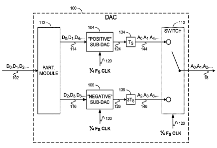
[0043] FIG. 2 illustrates an example digital-to-analog converter (DAC) 100
that is
operative to convert an input stream 102 of digital samples {Do, D1, D2, D3,
into the
output stream 18 of analog samples {A , Al, A2, A3, ...} at a sampling rate of
F.
[0044] FIG. 3 is a timing diagram of clock signals and data signals in the DAC
100.
[0045] The DAC 100 comprises a "positive" sub-DAC component 104, a "negative"
sub-
DAC component 106, and a controlled switch 110. The controlled switch 110 has
two inputs
(coupled to the outputs of the sub-DAC components 104, 106) and a single
output (the output
stream 18). (The controlled switch 110 is a specific example of the controlled
switch 10
described with respect to FIG. 1, where the number of sub-streams is precisely
two (N=2).)
[0046] The positive sub-DAC component 104 receives as input a first sub-stream
114 of
digital samples {Do, Di, D4, D5, ... }, and the negative sub-DAC component 106
receives as
input a second sub-stream 116 of digital samples {D2, D3, D6, D7, ...}. The
first sub-stream
114 is composed of pairs of adjacent digital samples such as {Do, D1, {D4,
D5}, and {D8,
D9}, and the second sub-stream 116 is composed of pairs of adjacent digital
samples such as
{D2, D3}, {D6, D7}, and {D io, Dil}. A partitioning module 112 comprised in
the DAC 100
is operative to partition the input stream 102 of digital samples into the
first sub-stream 114
and the second sub-stream 116, using any suitable technique. For example, the
partitioning
module 112 could reorder every four consecutive samples in the input stream
102 as {Do, D2,
CA 03101786 2020-11-26
WO 2019/239238
PCT/1B2019/054306
DI, D3, D4, D6, D5, D7, To obtain the first sub-stream 114 of digital
samples {130, DI,
D4, D5, ... }, the partitioning module 112 could apply a decimate-by-two
function to the
reordered samples. To obtain the second sub-stream 116 of digital samples {D2,
D3, D6, D7,
...}, the partitioning module 112 could delay a copy of the reordered samples
by a delay of
duration --Ts, and then apply a decimate-by-two function.
[0047] A clock signal 120 operating at -1/4Fs (and therefore having a period
of -4Ts) is
provided to the sub-DAC components 104, 106. The positive sub-DAC component
104
samples the first sub-stream 114 at rising edges and falling edges of the -
1/4Fs clock signal
120, thus converting the first sub-stream 114 into a first sub-stream 124 of
analog samples
{A0, Ai, A4, A5, ...}. The negative sub-DAC component 106 samples the second
sub-stream
116 at rising edges and falling edges of the -1/4Fs clock signal 120, thus
converting the
second sub-stream 116 into a second sub-stream 126 of analog samples {A2, A3,
A6, A7,
...}. An analog delay line 134 is operative to delay the first sub-stream 124
by a delay of
duration --Ts, yielding a first sub-stream 144 of delayed analog samples {A0,
Ai, A4, A5,
...}. An analog delay line 136 is operative to delay the second sub-stream 126
by a delay of
duration -3Ts, yielding a second sub-stream 146 of delayed analog samples {A2,
A3, A6, A7,
...}. (The first sub-stream 144 is a specific example of the first sub-stream
12 described with
respect to FIG. 1, and the second sub-stream 146 is a specific example of the
second sub-
stream 14 described with respect to FIG. 1.)
[0048] The -1/4Fs clock signal 120 is provided, with zero phase offset, to the
controlled
switch 110. The controlled switch 110 is controlled by rising edges and
falling edges of the
-1/4Fs clock signal 120, switching between a "positive" state in which the
first sub-stream
144 of delayed analog samples {A0, Ai, A4, A5, ...} contributes to the output
stream 18 and
a "negative" state in which the second sub-stream 146 of delayed analog
samples {A2, A3,
A6, A7, } contributes to the output stream 18. The resulting output stream 18
of analog
CA 03101786 2020-11-26
WO 2019/239238 PCT/1B2019/054306
11
samples {A0, AL A2, A3, A4, A5, A6, A7, } contains one analog sample in each
time
period of duration ¨TS.
[0049] As mentioned, the analog delay line 134 and the analog delay line 136
are operative
to introduce delays in the sub-streams of analog samples. These delays result
in the
arrangement of the timing of the "positive" states and "negative" states of
the controlled
switch 110 relative to the occurrence of data transitions between two adjacent
analog samples
in the first sub-stream 144 and in the second sub-stream 146.
[0050] While the controlled switch 110 is in the "positive" state, the data
transition in the
first sub-stream 144 from one analog sample to an adjacent analog sample is
captured. While
the controlled switch 110 is in the "negative" state, the data transition in
the second sub-
stream 146 from one analog sample to an adjacent analog sample is captured.
For example,
the analog samples Ao and Ai contribute one after the other to the output
stream 18 during a
single half-period of duration ¨2Ts of the ¨1/4Fs clock signal 120, and then
the analog
samples A2 and A3 contribute one after the other to the output stream 18
during a next single
half-period of duration ¨2Ts of the ¨1/4Fs clock signal 120.
[0051] The following time-table is helpful for understanding the operation of
the DAC 100
and the timing diagram illustrated in FIG. 3.
Time/Ts [0,1) [1,2) [2,3) [3,4) [4,5) [5,6)
I [6,7) [7,8)
sub-stream 144 Ao Ai A4 A5 A8
sub-stream 146 A2 A3 A6 A7
switch no state "positive" "negative" "positive" "negative"
output 18 Ao At A2 A3 Ai I As A6 A7
Table 1
[0052] By employing the mechanism described above with respect to FIG. 1, the
DAC 100
produces the output stream 18 at the rate of ¨Fs using clock signals operating
solely at ¨1/4Fs.
[0053] FIG. 4 illustrates an example digital-to-analog converter (DAC) 150
that is
operative to convert the input stream 102 of digital samples {Do, DI, D2, D3,
... 1 into the
output stream 18 of analog samples {Ao, Al, A2, A3, ... } at the sampling rate
of F.
CA 03101786 2020-11-26
WO 2019/239238
PCT/1B2019/054306
12
[0054] FIG. 5 is a timing diagram of clock signals and data signals in the DAC
150.
[0055] The DAC 150 is a variant of the DAC 100 illustrated in FIG. 2. In
contrast to the
DAC 100, there are no analog delay lines in the DAC 150. (The first sub-stream
124 is a
specific example of the first sub-stream 12 described with respect to FIG. 1,
and the second
sub-stream 126 is a specific example of the second sub-stream 14 described
with respect to
FIG. 1.)
[0056] In the DAC 150, the ¨Y4Fs clock signal 120 provided to the controlled
switch 110
has a 90 phase offset relative to the ¨1/4Fs clock signal 120 that is
provided to the sub-DAC
components 104, 106. The controlled switch 110 is controlled by rising edges
and falling
edges of the 90 phase offset ¨1/4Fs clock signal 120, switching between a
"positive" state in
which the first sub-stream 124 of analog samples {Ao, Al, A4, A5, ...}
contributes to the
output stream 18 and a "negative" state in which the second sub-stream 126 of
analog
samples {A2, A3, A6, A7, ...} contributes to the output stream 18. The
resulting output
stream 18 of analog samples {Ao, Al, A2, A3, A4, AS, A6, A7, ... } contains
one analog
sample in each time period of duration ¨Ts.
[0057] As illustrated, in the DAC 150, the ¨1/4Fs clock signal 120 provided to
the controlled
switch 110 has a 90 phase offset relative to the ¨1/4Fs clock signal 120 that
is provided to the
sub-DAC components 104, 106. This 90 phase offset results in the arrangement
of the
timing of the "positive" states and "negative" states of the controlled switch
110 relative to
the occurrence of data transitions between two adjacent analog samples in the
first sub-stream
124 and in the second sub-stream 126.
[0058] While the controlled switch 110 is in the "positive" state, the data
transition in the
first sub-stream 124 from one analog sample to an adjacent analog sample is
captured. While
the controlled switch 110 is in the "negative" state, the data transition in
the second sub-
stream 126 from one analog sample to an adjacent analog sample is captured.
For example,
the analog samples Ao and Al contribute one after the other to the output
stream 18 during a
single half-period of duration ¨2Ts of the 90 phase offset ¨1/4Fs clock
signal 120, and then
CA 03101786 2020-11-26
WO 2019/239238
PCT/IB2019/054306
13
the analog samples A2 and A3 contribute one after the other to the output
stream 18 during a
next single half-period of duration -2Ts of the 900 phase offset -1/4Fs clock
signal 120.
[0059] By employing the mechanism described above with respect to FIG. 1, the
DAC 150
produces the output stream 18 at the rate of -Fs using clock signals operating
solely at -1/4Fs.
[0060] FIG. 6 illustrates an example digital-to-analog converter (DAC) 200
that is
operative to convert the input stream 102 of digital samples {Do, DI, D2, D3,
... } into the
output stream 18 of analog samples {A0, Al, A2, A3, =.. } at the sampling rate
of F.
[0061] FIG. 7 is a timing diagram of clock signals and data signals in the DAC
200.
[0062] The DAC 200 comprises a "positive" sub-DAC component 204, a "zero" sub-
DAC
component 206, a "negative" sub-DAC component 208, and a controlled switch
210. The
controlled switch 210 has three inputs (coupled to the outputs of the sub-DAC
components
204, 206, 208) and a single output (the output stream 18). (The controlled
switch 210 is a
specific example of the controlled switch 10 described with respect to FIG. 1,
where the
number of sub-streams is precisely three (N=3).)
[0063] The positive sub-DAC component 204 receives as input a first sub-stream
214 of
digital samples {Do, DI, D6, D7, === }, the zero sub-DAC component 206
receives as input a
second sub-stream 216 of digital samples {D2, D3, D8, D9, ... }, and the
negative sub-DAC
component 208 receives as input a third sub-stream 218 of digital samples
1134, D5, D10,
Dii, 1. The first sub-stream 214 is composed of pairs of adjacent samples such
as {130,
Di}, {D6, D7}, and {D12. D13}, the second sub-stream 216 is composed of pairs
of adjacent
samples such as {D2, D3}, 1138, D91, and {D14, D15}, and the third sub-stream
218 is
composed of pairs of adjacent samples such as {D4, D5}, {Dio, Dil}, and {D16,
D17}. A
partitioning module 212 comprised in the DAC 200 is operative to partition the
input stream
102 of digital samples into the first sub-stream 214, the second sub-stream
216, and the third
sub-stream 218, using any suitable technique.
CA 03101786 2020-11-26
WO 2019/239238
PCT/1B2019/054306
14
[0064] A clock signal 220 operating at -1/4Fs (and therefore having a period
of -6Ts) is
provided to the sub-DAC components 204, 206, 208. The positive sub-DAC
component 204
samples the first sub-stream 214 at rising edges and falling edges of the -
1/4Fs clock signal
220, thus converting the first sub-stream 214 into a first sub-stream 224 of
analog samples
{Ao, Al, A6, A7, ...}. The zero sub-DAC component 206 samples the second sub-
stream 216
at rising edges and falling edges of the -%Fs clock signal 220, thus
converting the second
sub-stream 216 into a second sub-stream 226 of analog samples {A2, A3, A8, A9,
... }. The
negative sub-DAC component 208 samples the third sub-stream 218 at rising
edges and
falling edges of the -1/4Fs clock signal 220, thus converting the third sub-
stream 218 into a
third sub-stream 228 of analog samples {A4, A5, Aio, All, = = =1=
[0065] An analog delay line 234 is operative to delay the first sub-stream 224
by a delay of
duration -Ts, yielding a first sub-stream 244 of delayed analog samples {M,
Al, A6, A7,
}. An analog delay line 236 is operative to delay the second sub-stream 226 by
a delay of
duration -3Ts, yielding a second sub-stream 246 of delayed analog samples 1A2,
A3, A8, A9,
. An analog delay line 238 is operative to delay the third sub-stream 228 by a
delay of
duration -5Ts, yielding a third sub-stream 248 of delayed analog samples {A4,
A5, A10, All,
[0066] A three-state control signal 240 having a period of -6Ts is provided to
the
controlled switch 210. The controlled switch 210 is controlled by transitions
of the three-state
control signal 240, switching between a -positive" state in which the first
sub-stream 244 of
delayed analog samples {M, Al, A6, A7, ...} contributes to the output stream
18, a "zero"
state in which the second sub-stream 246 of delayed analog samples {A2, A3,
A8, A9, =
contributes to the output stream 18, and a "negative" state in which the third
sub-stream 248
of delayed analog samples {A4, A5, Aio, All, ...1 contributes to the output
stream 18. The
CA 03101786 2020-11-26
WO 2019/239238
PCT/1B2019/054306
resulting output stream 18 of analog samples {A0, At. A2, A3, A4, A5, A6, A7,
...} contains
one analog sample in each time period of duration ¨Ts.
[0067] As illustrated, the three-state control signal 240 has a zero-phase
offset relative to
the ¨1/6Fs clock signal 220 provided to the sub-DAC components 204, 206, 208.
The delays
introduced by the analog delay lines 234, 236, and 238 result in the
arrangement of the timing
of the "positive", "zero" and "negative" states of the controlled switch 210,
respectively,
relative to the occurrence of data transitions between two adjacent analog
samples in the first
sub-stream 244, the second sub-stream 246 and the third sub-stream 248.
[0068] While the controlled switch 210 is in the "positive" state, the data
transition in the
first sub-stream 244 from one analog sample to an adjacent analog sample is
captured. While
the controlled switch 210 is in the "zero" state, the data transition in the
second sub-stream
246 from one analog sample to an adjacent analog sample is captured. While the
controlled
switch 210 is in the "negative" state, the data transition in the third sub-
stream 248 from one
analog sample to an adjacent analog sample is captured. For example, the
analog samples AO
and Al contribute one after the other to the output stream 18 during a single
third-period of
duration ¨2Ts of the control signal 240, and then the analog samples A2 and A3
contribute
one after the other to the output stream 18 during a next single third-period
of duration ¨2Ts
of the control signal 240, and then the analog samples A4 and A5 contribute
one after the
other to the output stream 18 during a next single third-period of duration
¨2Ts of the control
signal 240.
[0069] The following time-table is helpful for understanding the operation of
the DAC 200
and the timing diagram illustrated in FIG. 7.
Time/Ts [0,1) [1,2) [2,3) I [3,4) [4,5) I
[5,6) I [6,7) [7,8)
sub-stream 244 Ao A1 A6 A7
sub-stream 246 A2 A3 Ag
sub-stream 248 A4 A5
switch 210 state "positive" "zero" "negative" "positive"
output 18 Ao At A2 A3 Aa As A6 A7
Table 2
CA 03101786 2020-11-26
WO 2019/239238
PCT/1B2019/054306
16
[0070] By employing the mechanism described above with respect to FIG. 1, the
DAC 200
produces the output stream at the rate of ¨Fs using clock signals operating
solely at ¨1/4Fs.
[0071] FIG. 8 illustrates an example digital-to-analog converter (DAC) 250
that is
operative to convert the input stream 102 of digital samples {Do, DI, D2, D3,
into the
output stream 18 of analog samples {Ao, Al, A2, A3, ...} at the sampling rate
of FS.
[0072] FIG. 9 is a timing diagram of clock signals and data signals in the DAC
250.
[0073] The DAC 250 is a variant of the DAC 200 illustrated in FIG. 5. In
contrast to the
DAC 200, there are no analog delay lines in the DAC 250.
[0074] In the DAC 250, a three-state control signal 260 having a period of
¨6Ts is provided
to the controlled switch 210. The controlled switch 210 is controlled by
transitions of the
three-state control signal 260, switching between a "positive" state in which
the first sub-
stream 224 of analog samples {Ao, AI, A6, A7, ... } contributes to the output
stream 18, a
"zero" state in which the second sub-stream 226 of analog samples {A2, A3, A8,
A9, = = = }
contributes to the output stream 18, and a "negative" state in which the third
sub-stream 228
of analog samples 1A4, A5, Ajo, All, ...I contributes to the output stream 18.
The resulting
output stream 18 of analog samples {Ao, Al, A2, A3, A4, As, A6, A7, ...}
contains one
analog sample in each time period of duration ¨Ts.
[0075] As illustrated, the three-state control signal 260 has a 60 phase
offset relative to the
-'/FS clock signal 220. This 60 phase offset results in the arrangement of
the timing of the
"positive", "zero" and "negative" states of the controlled switch 210 relative
to the
occurrence of data transitions between two adjacent analog samples in the
first sub-stream
224, the second sub-stream 226 and the third sub-stream 228.
[0076] While the controlled switch 210 is in the "positive" state, the data
transition in the
first sub-stream 224 from one analog sample to an adjacent analog sample is
captured. While
the controlled switch 210 is in the "zero" state, the data transition in the
second sub-stream
226 from one analog sample to an adjacent analog sample is captured. While the
controlled
CA 03101786 2020-11-26
WO 2019/239238
PCT/1B2019/054306
17
switch 210 is in the "negative" state, the data transition in the third sub-
stream 228 from one
analog sample to an adjacent analog sample is captured. For example, the
analog samples AO
and Al contribute one after the other to the output stream 18 during a single
third-period of
duration ¨2Ts of the three-state control signal 260, and then the analog
samples A2 and A3
contribute one after the other to the output stream 18 during a next single
third-period of
duration ¨2Ts of the three-state control signal 260, and then the analog
samples A4 and A5
contribute one after the other to the output stream 18 during a next single
third-period of
duration ¨2Ts of the three-state control signal 260.
[0077] By employing the mechanism described above with respect to FIG. 1, the
DAC 250
produces the output stream 18 at the rate of ¨Fs using clock signals operating
solely at ¨1/4Fs.
[0078] FIG. 10 illustrates an example sub-DAC 300 that is operative to convert
digital
samples into analog samples. The sub-DAC 300 may optionally be used as the
"positive"
sub-DAC 104 in DAC 100 or DAC 150 to convert the first sub-stream 114 of
digital samples
{Do, Di, D4, D5, ...} into the first sub-stream 124 of analog samples {Ao, Al,
A4, A5, ...} at
a sampling rate of V2Fs.
[0079] FIG. 11 is a timing diagram of clock signals and data signals in the
sub-DAC 300.
[0080] The sub-DAC 300 comprises an "even" sub-sub-DAC component 304, an "odd"
sub-DAC component 306, and an analog multiplexer (AMUX) component 310. The
AMUX
component 310 has two inputs (coupled to the outputs of the sub-sub-DAC
components 304,
306) and a single output (the first sub-stream 124).
[0081] The even sub-sub-DAC component 304 receives as input a first sub-sub-
stream 314
of digital samples {Do, D4, Ds, and the odd sub-sub-DAC component 306
receives as
input a second sub-sub-stream 316 of digital samples {Di, D5, D9, A
partitioning
module 312 is operative to partition the first sub-stream 114 of digital
samples into the first
sub-sub-stream 314 and the second sub-sub-stream 316, using any suitable
technique. For
example, the first sub-stream 114 could be duplicated, a delay buffer (not
shown) could delay
CA 03101786 2020-11-26
WO 2019/239238
PCT/1B2019/054306
18
one copy of the first sub-stream 114 by a duration of ¨Ts, and decimator
elements (not
shown) could remove every other sample from the copies of the first sub-stream
114.
[0082] A clock signal 320 operating at ¨1/4Fs (and therefore having a period
of ¨8Ts) is
provided to the sub-sub-DAC components 304, 306. The ¨1/8Fs clock signal 320
provided to
the odd sub-sub-DAC component 306 has a 90 phase offset relative to the
¨1/4.Fs clock signal
320 provided to the even sub-sub-DAC component 304. The even sub-sub-DAC
component
304 samples the first sub-sub-stream 314 at rising edges and falling edges of
the ¨1/2Fs clock
signal 320, thus converting the first sub-sub-stream 314 into a first sub-sub-
stream 324 of
analog samples {Ao, A4, Ag, ...}. The odd sub-DAC component 306 samples the
second sub-
sub-stream 316 at rising edges and falling edges of the 90 phase offset
¨1/4Fs clock signal
320, thus converting the second sub-sub-stream 316 into a second sub-sub-
stream 326 of
analog samples {Ai, A5, A9,
[0083] The ¨1/4Fs clock signal 120 is provided to the AMUX component 310. The
AMUX
component 310 is controlled by rising edges and falling edges of the ¨1/4Fs
clock signal 120,
switching between an "even" state in which the first sub-sub-stream 324 of
analog samples
{Ao, A4, A8, } contributes a single analog sample to the first sub-stream 124
and an "odd"
state in which the second sub-sub-stream 326 of analog samples {Ai, A5, A9,
... } contributes
a single analog sample to the first sub-stream 124. The resulting first sub-
stream 124 of
analog samples {Ao, Al, A4, A5, Ag, A9, ...} contains one analog sample in
each time period
of duration ¨2Ts.
[0084] The ¨1/4Fs clock signal 120 is offset by approximately 90 phase from
double the
¨1/8Fs clock signal 320. The ¨1/4Fs clock signal 120 is intentionally timed so
that no data
transition occurs between analog samples in the first sub-sub-stream 324 while
the AMUX
component 310 is in the "even" state, and no data transition occurs between
analog samples
in the second sub-sub-stream 326 while the AMUX component 310 is in the "odd"
state.
CA 03101786 2020-11-26
WO 2019/239238
PCT/IB2019/054306
19
Stated differently, all samples in the first sub-stream 124 are captured from
stable portions of
the sub-sub-streams 324 and 326.
[0085] FIG. 12 illustrates an example sub-DAC 350 that is operative to convert
digital
samples into analog samples. The sub-DAC 350 may optionally be used as the
"negative"
sub-DAC 106 in DAC 100 or DAC 150 to convert the second sub-stream 116 of
digital
samples {D2, D3, D6, D7, ... } into the second sub-stream 126 of analog
samples {A2, A3,
A6, A7, ...} at a sampling rate of V2Fs.
[0086] FIG. 13 is a timing diagram of clock signals and data signals in the
sub-DAC 350.
[0087] The sub-DAC 350 comprises an "even" sub-sub-DAC component 354, an "odd"
sub-DAC component 356, and an analog multiplexer (AMUX) component 360. The
AMUX
component 360 has two inputs (coupled to the outputs of the sub-sub-DAC
components 354,
356) and a single output (the second sub-stream 126).
[0088] The even sub-sub-DAC component 354 receives as input a first sub-sub-
stream 364
of digital samples {D2, D6, DIO, }, and the odd sub-sub-DAC component 356
receives as
input a second sub-sub-stream 366 of digital samples {D3, D7, Dii, ...}. A
partitioning
module 362 is operative to partition the second sub-stream 116 of digital
samples into the
first sub-sub-stream 364 and the second sub-sub-stream 366, using any suitable
technique.
For example, the second sub-stream 116 could be duplicated, a delay buffer
(not shown)
could delay one copy of the second sub-stream 116 by a duration of --Ts, and
decimator
elements (not shown) could remove every other sample from the copies of the
second sub-
stream 116.
[0089] The ¨'/8Fs clock signal 320 is provided to the sub-sub-DAC components
354, 356.
The ¨1/8Fs clock signal 320 provided to the odd sub-sub-DAC component 356 has
a 90
phase offset relative to the ¨1/4Fs clock signal 320 provided to the even sub-
sub-DAC
component 354. The even sub-sub-DAC component 354 samples the first sub-sub-
stream 364
at rising edges and falling edges of the 90 phase offset ¨Y8Fs clock signal
320, thus
converting the first sub-sub-stream 364 into a first sub-sub-stream 374 of
analog samples
CA 03101786 2020-11-26
WO 2019/239238
PCT/1B2019/054306
{A2, A6, } . The odd sub-DAC component 356 samples the second sub-sub-
stream
366 at rising edges and falling edges of the -'/Fs clock signal 320, thus
converting the
second sub-sub-stream 366 into a second sub-sub-stream 376 of analog samples
{A3, A7,
Ail, ..=}.
[0090] The ¨1/4Fs clock signal 120 is provided to the AMUX component 360. The
AMUX
component 360 is controlled by rising edges and falling edges of the ¨1/4Fs
clock signal 120,
switching between an "even" state in which the first sub-sub-stream 374 of
analog samples
{A2, A6, A10, = = =} contributes a single analog sample to the second sub-
stream 126 and an
"odd" state in which the second sub-sub-stream 376 of analog samples fA3, A7,
Ali, ...
contributes a single analog sample to the second sub-stream 126. The resulting
second sub-
stream 126 of analog samples {A2, A3, A6, A7, Ajo, A11, ...} contains one
analog sample in
each time period of duration ¨2Ts.
[0091] The ¨1/4Fs clock signal 120 is offset by approximately 90 phase from
double the
¨V8Fs clock signal 320. The --'/Fs clock signal 120 is intentionally timed so
that no data
transition occurs between analog samples in the first sub-sub-stream 374 while
the AMUX
component 360 is in the "even" state, and no data transition occurs between
analog samples
in the second sub-sub-stream 376 while the AMUX component 360 is in the "odd"
state.
Stated differently, all samples in the second sub-stream 126 are captured from
stable portions
of the sub-sub-streams 374 and 376.
[0092] Use of the sub-DACs 300 and 350 in the DAC 100 or in the DAC 150 will
increase
resilience to distortions as well as to time mismatches between sub-DACs, at a
cost of
increased complexity. The increased complexity involves providing a clock
signal at
approximately one quarter of the sampling rate (-1/4Fs), and the increased
complexity may be
deemed acceptable.
[0093] The following time-table is helpful for understanding use of the sub-
DACs 300 and
350 in the operation of the DAC 100.
CA 03101786 2020-11-26
WO 2019/239238 PCT/1B2019/054306
21
Time/Ts [0,1) [1,2) [2,3) 1 [3,4) [4,5) 1 [5,6)
[6,7) [7,8)
sub-sub-stream Ao A4 A8
324
sub-sub-stream A1 A5
326
AMUX 310 "even" "odd" "even" "odd"
"even"
state
sub-stream 124 Ao Al At As A8
sub-sub-stream A2 A6 Al0
374
sub-sub-stream A3 A7
376
AMUX 360 "even" "odd" "even" "odd" "even"
state
sub-stream 126 A2 A3 A6 A7 Al0
sub-stream 144
(delayed by Ts Ao Ai A4 A5
relative to sub-
stream 124)
sub-stream 146
(delayed by 3Ts A2 A3 A6
relative to sub-
stream 126)
switch 110 state "positive" "negative" "positive"
output 18 Ao Ai A2 A3 A4 As A6
Table 3
[0094] Sub-DACs similar to the sub-DACs 300 and 350 could be used as the
"positive"
sub-DAC, "zero" sub-DAC, and "negative" sub-DAC in the DAC 200 or in the DAC
250.
[0095] FIG. 14 is a block diagram illustration of an example transmitter 400
that employs
polarization-division multiplexing (PDM). A laser 402 is operative to generate
a continuous
wave (CW) optical carrier 404. A polarizing beam splitter 406 is operative to
split the CW
optical carrier 404 into orthogonally-polarized components 408, 410 (nominally
referred to as
the "X-polarization" component and the "Y-polarization" component) that are
modulated by
respective electrical-to-optical modulators 412, 414 to produce modulated
polarized optical
signals 416, 418 that are combined by a beam combiner 420, thus yielding an
optical signal
422.
[0096] A symbol source 424 is operative to generate a stream of symbols
representing data
to be transmitted in the optical signal 422. A digital signal processor (DSP)
426 is operative
to process the symbols output from the symbol source 424, for example,
performing one or
CA 03101786 2020-11-26
WO 2019/239238
PCT/1B2019/054306
22
more of pulse shaping, subcarrier multiplexing, chromatic dispersion pre-
compensation, and
distortion pre-compensation on the symbols. The DSP 426 is operative to
generate I and Q
digital drive signals 432 for the X-polarization to be converted by a DAC 434
into I and Q
analog drive signals 436 for the X-polarization that, after amplification by
amplifiers 438, are
used to drive the electrical-to-optical modulator 412. The DSP 426 is
operative to generate I
and Q digital drive signals 442 for the Y-polarization to be converted by a
DAC 444 into I
and Q analog drive signals 446 for the Y-polarization that, after
amplification by amplifiers
448, are used to drive the electrical-to-optical modulator 414.
[0097] The DACs described in this document could be used as the DAC 434 and
the DAC
444. For example, the I and Q digital drive signals 432 for the X-polarization
may be the
input stream 102 of digital samples {Do, DI, D2, D3, ...} and the land Q
analog drive signals
436 for the X-polarization may be the output stream 18 of analog samples {Ao,
Ai, A2, A3,
...}. For example, the I and Q digital drive signals 442 for the Y-
polarization may be the
input stream 102 of digital samples {Do, Di, D2, D3, ...} and the land Q
analog drive signals
446 for the Y-polarization may be the output stream 18 of analog samples {Ao,
AI, A2, A3,
[0098] Stated differently, each of the DAC 434, 444 may comprise two or more
sub-DACs,
and the streams of analog samples that are output from the two or more sub-
DACs may be
provided as inputs to a controlled switch that is a specific example of the
controlled switch 10
described with respect to FIG. 1. In some implementations, a sub-DAC may
employ the
architecture described with respect to FIG. 10 or FIG. 12.
[0099] In some implementations, the DSP 426 and the DACs 434, 444 are
comprised in a
CMOS module, and the amplifiers 438, 448 are comprised in a BiCMOS module.
[0100] In other implementations, when the interconnect between blocks does not
support
the full bandwidth, the controlled switches of the DACs 434, 444 may be
separate from the
CMOS module that comprises the DSP 426 and the other components (including the
sub-
DACs) of the DACs 434, 444. For example, the controlled switches may be
comprised in
another CMOS module, or a BiCMOS module, or I-IBT. For example, the controlled
switches
may be co-packaged with the electrical-to-optical modulator 412, 414 or the
driver.
CA 03101786 2020-11-26
WO 2019/239238
PCT/1B2019/054306
23
[0101] For simplicity of explanation, perfect analog switches were used in the
examples,
with a square clock. At high frequencies, the clock will generally consist of
a fundamental
along with one or two harmonics. The controlled switch may be implemented with
nonlinear
electrical, electro-optic, or optical elements, such as CMOS field effect
transistors (FETs) or
diodes, bipolar transistors or diodes, heterojunction bipolar transistors
(HBTs), electro-
absorption (EA) modulators, phase modulators, or semiconductor optical
amplifier (SOA)
structures. The switching function may be substantially a multiplication by
the clock voltage
or may include strong nonlinear functional terms.
[0102] The techniques described in this document may be used to convert
integer sub-
streams into a voltage stream, in CMOS. However, other instantiations may be
used. For
example, current sub-streams may be converted to an optical E-Field stream, as
was
described in US Patent No. 7277603 to Roberts et al. An integer sub-stream may
be
combined with a voltage sub-stream to produce a voltage stream. The analog
characteristic of
the stream that is being created may be an optical or electrical phase, or
other modulation of
an input analog signal.
[0103] A series of integer values that represent a time-series signal may be
instantiated in
parallel circuits or any other pre-determined pattern.
[0104] The scope of the claims should not be limited by the details set forth
in the
examples, but should be given the broadest interpretation consistent with the
description as a
whole.