Note: Descriptions are shown in the official language in which they were submitted.
CA 03101791 2020-11-26
WO 2019/232232 PCT/US2019/034688
ENERGY HARVESTING DEVICES AND SENSORS, AND METHODS OF
MAKING AND USE THEREOF
CROSS REFERENCE TO RELATED APPLICATIONS
This application claims priority to, and the benefit of, both United States
Provisional
Patent Application Serial No. 62/677,826 filed on May 30, 2018, and United
States Provisional
Patent Application Serial No. 62/741,234 filed on October 4, 2018, both of
which are
incorporated by reference as if set forth fully herein.
STATEMENT REGARDING FEDERALLY SPONSORED RESEARCH
Neither the priority applications nor this application used government funds
or benefitted
from government sponsored research.
FIELD
The disclosed technology generally relates to energy harvesting devices and
sensors, and
methods of making and use thereof.
BACKGROUND
Vibration energy harvesting is the practice of capturing vibration energy from
external
vibration sources (e.g. vehicles, machines, buildings, and human motions).
This captured energy
can then be used for various applications. In certain approaches to vibration
energy harvesting, a
plate is fixed at one end and will vibrate up and down between two extremes
when it is excited.
By flexing and oscillating between the two extremes, the strain/stress
developed on the surface
of the plate can be used to generate energy. Vibrations at the atomic scale
are omnipresent, even
in a mechanically quiet environment. This is due to the material being held at
some temperature
above absolute zero, and are called thermal vibrations. It is with respect to
these and other
considerations that the various embodiments described below are presented.
SUMMARY
In accordance with the purposes of the disclosed devices and methods, as
embodied and
broadly described herein, the disclosed subject matter relates to energy
harvesting devices and
sensors, and methods of making and use thereof.
In one embodiment, a system for harvesting vibrational energy includes a free-
standing
membrane connected to one or more supports and has a first surface that is
unobstructed and free
to vibrate in response to ambient energy. Vibration of the membrane defines
cyclical ripple
1
CA 03101791 2020-11-26
WO 2019/232232 PCT/US2019/034688
formations along the first surface, wherein each ripple formation alternates
between a peak and a
trough in a respective window region of a plurality of window regions of the
membrane. A
scanning tunneling microscope (STM) is connected to the system and has a tip
and a voltage
source. The STM tip is positioned proximate the membrane to define a
respective capacitive
region of charges between the tip of the STM and the window regions of the
membrane. A
distance between the tip of the STM and each respective window region of the
window regions
of the membrane varies with respective peaks and troughs. The capacitive
region between the
tip of the STM and each window region of the membrane stores and emits the
charges in cycles
according to the distance between the tip and the respective window region. A
fixed storage
capacitor is connected to the membrane and receives emitted charges from the
capacitive region
when the distance between the tip of the STM and each window region is
increasing during
ripple peak periods. The voltage source delivers charges to the capacitive
region when the
distance between the tip of the STM and a respective window region is
decreasing during ripple
trough periods.
In another embodiment, the disclosure provides a system for converting
vibrational
energy to a current output with a free-standing membrane connected to one or
more supports and
comprising a first surface that is unobstructed and free to vibrate in
response to ambient energy.
Vibration of the membrane defines cyclical ripple formations along the first
surface, wherein
each ripple formation alternates between a peak and a trough in a respective
window region of a
plurality of window regions of the membrane. A scanning tunneling microscope
(STM) with a
tip is positioned proximate the membrane, and the STM includes a voltage
source setting a
setpoint current between the tip and the membrane to define a respective
capacitive region of
charges between the tip and the window regions of the membrane. A distance
between the tip of
the microscope and each window region of the membrane varies with respective
peaks and
troughs, and the capacitive region stores and emits the charges in cycles in
response to the
distance between the tip and the window regions and pursuant to tunneling of
additional charges
through the capacitive region. A fixed storage capacitor is connected to the
membrane and
receives emitted charges and additional tunneling charges from the capacitive
region when the
distance between the tip of the microscope and a respective window region is
increasing during
ripple peak periods in the respective window region.
In yet another embodiment, a system for converting vibrational energy to a
current output
includes a current harvesting circuit in a substrate, wherein the current
harvesting circuit
comprises a common metal contact connected by respective matching oriented
diodes to a
voltage source and a fixed storage capacitor. A free-standing membrane extends
over at least the
2
CA 03101791 2020-11-26
WO 2019/232232 PCT/US2019/034688
common metal contact in the current harvesting circuit, such that the common
metal contact is
separated from the membrane by a stand-off support and faces a first surface
of the membrane to
define a capacitive region between the common metal contact and the first
surface of the
membrane. The first surface of the membrane is unobstructed and free to
vibrate in response to
ambient energy, wherein vibration of the membrane defines cyclical ripple
formations along the
first surface, and wherein each ripple formation alternates between a peak and
a trough relative
to the common contact. The capacitive region between the common contact and
the membrane
accumulates charges between the common contact and the membrane, and the
common contact
switches a current output of accumulated charges across one of the respective
diodes to direct the
current output to either the voltage source or the fixed storage capacitor in
response to the
cyclical ripple formations in the membrane.
In another non-limiting embodiment of this disclosure, a method of assembling
an energy
harvesting circuit includes forming a capacitive region in the energy
harvesting circuit by
defining a first capacitor plate having an initial separation distance with
respect to a first surface
of a free-standing membrane, wherein the first surface of the free-standing
membrane defines a
second capacitor plate, then connecting the first capacitor plate to a voltage
source configured to
induce charge accumulation in the capacitive region. Next, the membrane is
positioned relative
to the first capacitor plate such that the membrane is unobstructed and free
to vibrate in response
to ambient energy, wherein vibration of the membrane defines cyclical ripple
formations along
the first surface, and wherein each ripple formation alternates between a peak
and a trough
relative to the first capacitor plate to change the initial separation
distance. The method includes
discharging the capacitive region across a respective diode to direct
accumulated charges to
either the voltage source or a load, wherein discharging the capacitive region
comprises directing
the charges to the voltage source and directing the charges to the load during
a peak.
Another embodiment discloses a method of assembling an energy harvesting
circuit by
impregnating an insulating layer of a freestanding membrane with fixed charge
carriers and
forming a capacitive region in the energy harvesting circuit by defining a
first capacitor plate
having an initial separation distance with respect to a first surface of the
free-standing
membrane. The first surface of the free-standing membrane defines a second
capacitor plate
having the fixed charge carriers. The method further allows for positioning
the membrane
relative to the first capacitor plate such that the membrane is unobstructed
and free to vibrate in
response to ambient energy and change a capacitance of the capacitive region,
wherein vibration
of the membrane defines cyclical ripple formations along the first surface,
and wherein each
ripple formation alternates between a peak and a trough relative to the first
capacitor plate to
3
CA 03101791 2020-11-26
WO 2019/232232 PCT/US2019/034688
change the initial separation distance. During periods of vibration,
accumulated charge is
directed from the first capacitor plate into the capacitive region. The
accumulated charge may be
discharged from the capacitive region across at least one of a resistive load
and a fixed storage
capacitor.
Additional advantages of the disclosed devices and methods will be set forth
in part in
the description which follows, and in part will be obvious from the
description. The advantages
of the disclosed devices will be realized and attained by means of the
elements and combinations
particularly pointed out in the appended claims. It is to be understood that
both the foregoing
general description and the following detailed description are exemplary and
explanatory only
and are not restrictive of the disclosed devices and methods, as claimed.
The details of one or more embodiments of the invention are set forth in the
accompanying drawings and the description below. Other features, objects, and
advantages of
the invention will be apparent from the description and drawings, and from the
claims.
BRIEF DESCRIPTION OF THE DRAWINGS
The accompanying drawings, which are incorporated and constitute a part of
this
specification, illustrate several aspects of the disclosure, and together with
the description, serve
to explain the principles of the disclosure.
FIG. 1A is a perspective view of a membrane subject to ripple formation as
disclosed
herein.
FIG. 1B is a schematic of an energy harvesting and energy sensing system as
set forth in
this disclosure.
FIG. 2A is a top view of a membrane subject to a compressive force that
interacts with
vibrational ripple formation according to this disclosure.
FIG. 2B is a side view of a membrane subject to oppositely directed lateral
compressive
forces and upward vibrational forces at points along an edge of a portion of a
membrane
showing vibrational ripple formation according to this disclosure.
FIG. 2C is a side view of a membrane subject to an oppositely directed lateral
compressive forces and oppositely directed vibrational forces at points along
an edge of a
membrane showing vibrational ripple formation according to this disclosure.
FIG. 2D is a side view of a taut membrane displaced into a ripple formation by
compressive and vibrational forces as described herein.
4
CA 03101791 2020-11-26
WO 2019/232232 PCT/US2019/034688
FIG. 3A is a schematic view of a variable capacitor circuit having one fixed
plate and one
displaceable plate as set forth herein.
FIG. 3B is a plot of current in nanoamps discharged from a storage capacitor
connected
to the circuit of FIG. 3A.
FIG. 4A is a schematic diagram of a variable capacitance across one fixed
capacitor plate
and one displaceable capacitor plate charging due to a voltage source as set
forth herein.
FIG. 4B is a schematic diagram of a variable capacitance across one fixed
capacitor plate
and one displaceable capacitor plate discharging to a fixed storage capacitor
load and charging
the voltage source as set forth herein.
FIG. 4C is a schematic diagram of a storage capacitor discharging across a
resistive
ammeter load as set forth herein.
FIG. 5 is a plot of charge accumulated in nano-Coulombs in a storage capacitor
after
operating the circuit in Fig. 4A and 4B for the time shown and fthe tunneling
current set points
for the microscope as disclosed herein.
FIG. 6 is a plot of energy in pico-Joules stored in a storage capacitor after
operating the
circuit in Fig. 4A and 4B for the time shown and fthe tunneling current set
point currents for the
microscope as disclosed herein.
FIG. 7 is a plot of charge stored in nano-Coulombs in the storage capacitor
after 50
second energy harvesting time at numerous set point currents for the
microscope as disclosed
herein.
FIG. 8 is a plot of charge stored in nano-Coulombs in the storage capacitor
after 100
second harvest time at numerous set point currents for the microscope as
disclosed herein.
FIG. 9 is a plot of charge stored in nano-Coulombs in the storage capacitor
after 200
second harvest time at numerous set point currents for the microscope as
disclosed herein.
FIG. 10 is a plot of charge stored in nano-Coulombs in the storage capacitor
after 500
second harvest time at numerous set point currents for the microscope as
disclosed herein.
FIG. 11 is a schematic view illustrating sources of discharged current and
tunneling
current across a variable capacitor that inherently incorporates a variable
resistance as disclosed
herein.
FIG. 12A is a schematic view of a sensor circuit utilizing an ammeter to
measure either
or both emitted current and tunneling current across a variable capacitance
region as described
herein.
FIG. 12B is a plot of discharged current over time from a variable capacitor
across an
ammeter when using freestanding graphene as disclosed herein.
CA 03101791 2020-11-26
WO 2019/232232 PCT/US2019/034688
FIG. 12C is a plot of tunneling current over time from a variable capacitor
across an
ammeter when using rigid graphene as disclosed herein.
FIG. 12D is a plot of standard deviation values for discharged current for
both
freestanding graphene and rigid graphene as a function of setpoint tunneling
current for a
scanning tunneling microscope as disclosed herein.
FIG. 12E is a schematic view of a sensor circuit with inherent parasitic
capacitance
utilizing an ammeter to measure current across a variable capacitance region
as described herein.
FIG. 12F is a plot of harvested current over time from a variable capacitor
across an
ammeter for both freestanding graphene and rigid graphene as disclosed herein.
FIG. 12G is a plot of standard deviation values for discharged current for
free standing
graphene membrane and a rigid sample of graphene on silicon carbide as a
function of setpoint
current for a scanning tunneling microscope as disclosed herein.
FIG. 12H is a schematic view of a sensor circuit utilizing an ammeter to
measure either
or both emitted current and tunneling current across a variable capacitance
region as described
herein.
FIG. 121 is a plot of harvested current with no tunneling current over time
from a variable
capacitor across an ammeter for three different bias voltages as disclosed
herein.
FIG. 12J is a plot of harvested current with no tunneling current as a
function of setpoint
bias voltage for a scanning tunneling microscope as disclosed herein.
FIG. 13 is a plot of maximum charge stored in nano-Coulombs in a storage
capacitor as
disclosed herein during various harvest times.
FIG. 14 is a plot of maximum energy in pico-Joules stored in a fixed capacitor
as herein
during various harvesting times.
FIG. 15 is a plot of maximum charge stored in nano-Coulombs in a fixed storage
capacitor as disclosed herein during various harvesting times across different
tunneling set point
currents.
FIG. 16 is a plot of energy stored in a fixed storage capacitor as disclosed
herein during
various harvesting times across different set point currents.
FIG. 17A is a schematic view of an array of variable capacitors in an energy
harvesting
circuit according to the disclosure herein.
FIG. 17B is a cross section view of a layered array of variable capacitors in
an energy
harvesting circuit according to the disclosure herein.
FIG. 18 (a) Illustration of naturally occurring ripples in freestanding
graphene. (b) Raw
STM height-time data series acquired over 10,000 s shown with a trend line
obtained from a
6
CA 03101791 2020-11-26
WO 2019/232232 PCT/US2019/034688
low-pass Wiener filter algorithm to isolate large-scale fluctuations. (c)
Measured tunneling
current associated with the data shown in (b). (d) Background subtracted
height-time data
showing only the fluctuations in the membrane height. The data shown at zero
height is the
control data acquired from a rigid graphene sample. (e) Height autocorrelation
function
(AAAAAA) calculated from the background subtracted data shown in (d). (f)
Power spectral
density (PPPPPP) calculated from the STM data shown in (d).
FIG. 19 (a) Molecular dynamics convex ripple geometry, (b) simulation output
height-
time series, (c) height autocorrelation function, and (d) power spectral
density of height-time
series.
FIG. 20 (a) Simulation output height-time data of the spin-membrane model and
configurations at three different times, (b) height autocorrelation function
ACF, and (c) power
spectral density.
FIGS. 21A-21R are iterative illustrations of steps for forming an energy
harvesting
circuit according to this disclosure using electron beam patterning.
FIGS. 22A-22R are iterative illustrations of steps for forming an energy
harvesting
circuit according to this disclosure using photolithography.
FIG. 23 is a top perspective view of an energy transducer formed in a
substrate according
to this disclosure.
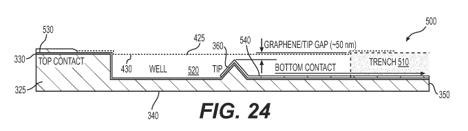
FIG. 24 is a side view of a cross section of the transducer of FIG. 23.
FIG. 25 is a top view of a left side section of the transducer of FIG. 24.
FIG. 26 is a side view of the cross section of the transducer of FIG. 23.
FIG. 27 is a top perspective view of the energy transducer of FIG. 23 with a
detailed inset
figure showing a closer view of a tip and well region according to this
disclosure.
DETAILED DESCRIPTION
The devices and methods described herein may be understood more readily by
reference
to the following detailed description of specific aspects of the disclosed
subject matter and the
Examples included therein.
Before the present devices and methods are disclosed and described, it is to
be
understood that the aspects described below are not limited to the details of
construction and
arrangement of components set forth in the following description or
illustrated in the drawings.
The disclosed technology is capable of other embodiments and of being
practiced or carried out
in various ways.
7
CA 03101791 2020-11-26
WO 2019/232232 PCT/US2019/034688
In the following description, references are made to the accompanying drawings
that
form a part hereof and that show, by way of illustration, specific embodiments
or examples.
It is also to be understood that the terminology used herein is for the
purpose of
describing particular aspects only and is not intended to be limiting. In
describing example
embodiments, terminology will be resorted to for the sake of clarity. It is
intended that each
term contemplates its broadest meaning as understood by those skilled in the
art and includes all
technical equivalents that operate in a similar manner to accomplish a similar
purpose. It is also
to be understood that the mention of one or more steps of a method does not
preclude the
presence of additional method steps or intervening method steps between those
steps expressly
identified. Steps of a method may be performed in a different order than those
described herein
without departing from the scope of the disclosed technology. Similarly, it is
also to be
understood that the mention of one or more components in a device or system
does not preclude
the presence of additional components or intervening components between those
components
expressly identified.
Also, throughout this specification, various publications are referenced. The
disclosures
of these publications in their entireties are hereby incorporated by reference
into this application
in order to more fully describe the state of the art to which the disclosed
matter pertains. The
references disclosed are also individually and specifically incorporated by
reference herein for
the material contained in them that is discussed in the sentence in which the
reference is relied
upon.
The specification makes references to numerous electrical charges of opposite
polarity
along with collection of certain positive and negative charges on identified
hardware. Nothing in
this specification limits the disclosure to any one arrangement of positive or
negative polarity in
circumstances where an opposite polarity may also be arranged.
The specification further references peaks and troughs of a freestanding
membrane
subject to rippling effects due to outside energy forces, and whether a
certain structure of the
membrane is a peak or a trough depends up perspective as well as the
membrane's position
relative to another structure. Accordingly, nothing in this detailed
specification requires any
particular orientation of structures or hardware, and the terms "peaks,"
"troughs," and "ripples"
are not limited to any one orientation but are for description purposes only.
Definitions
In this specification and in the claims that follow, reference will be made to
a number of
terms, which shall be defined to have the following meanings:
8
CA 03101791 2020-11-26
WO 2019/232232 PCT/US2019/034688
Throughout the description and claims of this specification the word
"comprise" and
other forms of the word, such as "comprising" and "comprises," means including
but not limited
to, and is not intended to exclude, for example, other additives, components,
integers, or steps.
As used in the description and the appended claims, the singular forms "a,"
"an," and
"the" include plural referents unless the context clearly dictates otherwise.
Thus, for example,
reference to "a composition" includes mixtures of two or more such
compositions, reference to
"the compound" includes mixtures of two or more such compounds, reference to
"an agent"
includes mixture of two or more such agents, and the like.
It is understood that throughout this specification the identifiers "first"
and "second" are
used solely to aid the reader in distinguishing the various components,
features, or steps of the
disclosed subject matter. The identifiers "first" and "second" are not
intended to imply any
particular order, amount, preference, or importance to the components or steps
modified by these
terms.
The term "or combinations thereof' as used herein refers to all permutations
and
combinations of the listed items preceding the term. For example, "A, B, C, or
combinations
thereof' is intended to include at least one of: A, B, C, AB, AC, BC, or ABC,
and if order is
important in a particular context, also BA, CA, CB, CBA, BCA, ACB, BAC, or
CAB.
Continuing with this example, expressly included are combinations that contain
repeats of one or
more item or term, such as BB, AAA, AB, BBC, AAABCCCC, CBBAAA, CABABB, and so
forth. The skilled artisan will understand that typically there is no limit on
the number of items
or terms in any combination, unless otherwise apparent from the context.
Energy Harvesting Devices and Sensors
Described herein are energy harvesting devices 100 and sensors 195. The energy
harvesting devices and sensors can comprise a membrane 265 disposed on a
substrate 258,
wherein the membrane 225 comprises a two-dimensional (2D) material and one or
more ripples
having peaks 286 and troughs 289 as shown in Figure 1A. As further illustrated
in Figure 1A,
the substrate may be a grid 258 defining grid cells across a span of the
substrate to outline
window regions 269 of the overlaying membrane 265 within each cell as
discussed herein.
In an example embodiment, an energy harvesting device 100 having a power
source 105,
118, 200 for ambient vibration energy harvesting is disclosed, having an
atomic two-dimensional
membrane 265 for buckling at a relatively low frequency. The anomalous
vibrational kinetic
energy of these two-dimensional materials, if used as the active component of
an energy
harvesting device 100, can provide superior energy production when compared to
existing
technology. For example, in current silicon microelectromechanical (MEM)
vibration energy
9
CA 03101791 2020-11-26
WO 2019/232232 PCT/US2019/034688
harvesting technology, the active component may be an etch silicon platform.
This platform will
not spontaneously vibrate or mechanically buckle because it is too rigid.
"Mechanical buckling"
is understood in this disclosure as non-linear phenomenon. The prior
approaches of silicon
MEM structures are linear response devices. In contrast, the membrane 265 of
the energy
harvesting devices 100 described herein can spontaneously vibrate and
mechanically buckle.
The two-dimensional material can, for example, comprise graphene, MoS2, MoSe2,
WS2,
WSe2, ReS2, ReSe2, Boron Nitride (BN) or a combination thereof. In certain
examples, the two-
dimensional material can comprise graphene. The graphene may include monolayer
materials,
bi-layer materials, tri-layer materials, and multi-layer materials. Though the
example
embodiments herein indicate that one non-limiting material for the
freestanding membrane is
graphene, any of the materials discussed herein may be a viable option as well
for the
freestanding membrane. These layers may be stacked on one another in arbitrary
or specific
crystallographic orientations, which may enhance the vibrational properties.
The identity of the two-dimensional material can be selected based on a
variety of
factors. For example, the bending stiffness varies between the different two-
dimensional
materials and therefore different vibration frequencies would be available.
Also, the electrical
conductivity of the various two-dimensional materials varies considerably,
which can control the
efficiency of harvesting energy using an electrostatic approach. Accordingly,
the identity of the
two-dimensional material can be selected to control one or more of these
parameters.
In some examples, the membrane 265 can comprise freestanding graphene which
has a
substantially large velocity component in the velocity probability
distribution. In some
examples, the membrane 265 can exhibit perpetual non-linear movement at room
temperature.
The membrane 265 can, for example, have an average thickness of 0.3 nanometers
(nm)
or more (e.g., 0.4 nm or more, 0.5 nm or more, 0.6 nm or more, 0.7 nm or more,
0.8 nm or more,
0.9 nm or more, 1.0 nm or more, 1.1 nm or more, 1.2 nm or more, 1.3 nm or
more, 1.4 nm or
more, 1.5 nm or more, 1.6 nm or more, 1.7 nm or more, 1.8 nm or more, 1.9 nm
or more, 2.0 nm
or more, 2.1 nm or more, 2.2 nm or more, 2.3 nm or more, 2.4 nm or more, or
2.5 nm or more).
In some examples, the membrane 265 can have an average thickness of 3.0 nm or
less (e.g., 2.9
nm or less, 2.8 nm or less, 2.7 nm or less, 2.6 nm or less, 2.5 nm or less,
2.4 nm or less, 2.3 nm
or less, 2.2 nm or less, 2.1 nm or less, 2.0 nm or less, 1.9 nm or less, 1.8
nm or less, 1.7 nm or
less, 1.6 nm or less, 1.5 nm or less, 1.4 nm or less, 1.3 nm or less, 1.2 nm
or less, 1.1 nm or less,
1.0 nm or less, 0.9 nm or less, 0.8 nm or less, 0.7 nm or less, 0.6 nm or
less, or 0.5 nm or less).
The average thickness of the membrane 265 can range from any of the minimum
values
described above to any of the maximum values described above. For example, the
membrane
CA 03101791 2020-11-26
WO 2019/232232 PCT/US2019/034688
265 can have an average thickness of from 0.3 nm to 3.0 nm (e.g., from 0.3 nm
to 2.5 nm, from
0.3 nm to 2.0 nm, from 0.3 nm to 1.5 nm, form 0.3 nm to 1.0 nm, or from 0.3 nm
to 0.6 nm).
The membrane 265 can, for example, have an average lateral dimension of 0.1
microns
(pm) or more (e.g., 0.5 pm or more, 1 pm or more, 1.5 pm or more, 2 pm or
more, 2.5 pm or
more, 3 pm or more, 3.5 pm or more, 4 pm or more, 4.5 pm or more, 5 pm or
more, 6 pm or
more, 7 pm or more, 8 pm or more, 9 pm or more, 10 pm or more, 15 pm or more,
20 pm or
more, 25 pm or more, 30 pm or more, 35 pm or more, 40 pm or more, 45 pm or
more, 50 pm or
more, 60 pm or more, 70 pm or more, or 80 pm or more). In some examples, the
membrane 265
can have an average lateral dimension of 100 pm or less (e.g., 90 pm or less,
80 pm or less, 70
pm or less, 60 pm or less, 50 pm or less, 45 pm or less, 40 pm or less, 35 pm
or less, 30 pm or
less, 25 pm or less, 20 pm or less, 15 pm or less, 10 pm or less, 9 pm or
less, 8 pm or less, 7 pm
or less, 6 pm or less, 5 pm or less, 4.5 pm or less, 4 pm or less, 3.5 pm or
less, 3 pm or less, 2.5
pm or less, 2 pm or less, 1.5 pm or less, or 1 pm or less). The average
lateral dimension of the
membrane 265 can range from any of the minimum values described above to any
of the
maximum values described above. For example, the membrane 265 can have an
average lateral
dimension of from 0.1 microns to 100 microns (e.g., from 0.1 pm to 50 pm, from
50 pm to 100
pm, from 0.1 pm to 20 pm, from 20 pm to 40 pm, from 40 pm to 60 pm, from 60 pm
to 80 pm,
from 80 pm to 100 pm, from 0.5 pm to 95 pm, or from 10 pm to 90 pm).
In some examples, the membrane 265 can have a tension per unit length of 0.0
Newtons
per meter (N/m) or more (e.g., 0.01 N/m or more, 0.02 N/m or more, 0.03 N/m or
more, 0.04
N/m or more, 0.05 N/m or more, 0.06 N/m or more, 0.07 N/m or more, 0.08 N/m or
more, 0.09
N/m or more, 0.10 N/m or more, 0.11 N/m or more, 0.12 N/m or more, 0.13 N/m or
more, 0.14
N/m or more, 0.15 N/m or more, 0.20 N/m or more, 0.25 N/m or more, 0.30 N/m or
more, 0.35
N/m or more, 0.40 N/m or more, 0.45 N/m or more, 0.50 N/m or more, 0.60 N/m or
more, 0.70
N/m or more, 0.80 N/m or more, 0.90 N/m or more, 1.0 N/m or more, 1.5 N/m or
more, 2.0 N/m
or more, 2.5 N/m or more, 3.0 N/m or more, 3.5 N/m or more, 4.0 N/m or more,
4.5 N/m or
more, 5.0 N/m or more, 6.0 N/m or more, or 7.0 N/m or more). In some examples,
the membrane
265 can have a tension per unit length of 10.0 N/m or less (e.g., 9.0 N/m or
less, 8.0 N/m or less,
7.0 N/m or less, 6.0 N/m or less, 5.0 N/m or less, 4.5 N/m or less, 4.0 N/m or
less, 3.5 N/m or
less, 3.0 N/m or less, 2.5 N/m or less, 2.0 N/m or less, 1.5 N/m or less, 1.0
N/m or less, 0.90 N/m
or less, 0.80 N/m or less, 0.70 N/m or less, 0.60 N/m or less, 0.50 N/m or
less, 0.45 N/m or less,
0.40 N/m or less, 0.35 N/m or less, 0.30 N/m or less, 0.25 N/m or less, 0.20
N/m or less, 0.15
N/m or less, 0.14 N/m or less, 0.13 N/m or less, 0.12 N/m or less, 0.11 N/m or
less, 0.10 N/m or
less, 0.09 N/m or less, 0.08 N/m or less, 0.07 N/m or less, 0.06 N/m or less,
or 0.05 N/m or less).
11
CA 03101791 2020-11-26
WO 2019/232232 PCT/US2019/034688
The tension per unit length of the membrane 265 can range from any of the
minimum values
described above to any of the maximum values described above. For example, the
membrane
265 can have a tension per unit length of from 0.0 to 10.0 N/m (e.g., from 0.0
N/m to 8.0 N/m,
from 0.0 N/m to 5.0 N/m, from 0.0 N/m to 3.0 N/m, from 0.0 N/m to 1.0 N/m,
from 0.0 to 0.5
N/m, from 0.0 to 0.3 N/m, or from 0.03 N/m to 0.12 N/m). The tension can be
measured using
atomic force microscopy.
The one or more ripples can, for example, have an average length of 1 nm or
more (e.g.,
2 nm or more, 3 nm or more, 4 nm or more, 5 nm or more, 6 nm or more, 7 nm or
more, 8 nm or
more, 9 nm or more, 10 nm or more, 15 nm or more, 20 nm or more, 25 nm or
more, 30 nm or
more, 35 nm or more, 40 nm or more, 45 nm or more, 50 nm or more, 55 nm or
more, 60 nm or
more, 65 nm or more, 70 nm or more, 75 nm or more, or 80 nm or more). In some
examples, the
one or more ripples can have an average length of 100 nm or less (e.g., 95 nm
or less, 90 nm or
less, 85 nm or less, 80 nm or less, 75 nm or less, 70 nm or less, 65 nm or
less, 60 nm or less, 55
nm or less, 50 nm or less, 45 nm or less, 40 nm or less, 35 nm or less, 30 nm
or less, 25 nm or
less, 20 nm or less, 15 nm or less, 10 nm or less, 9 nm or less, 8 nm or less,
7 nm or less, 6 nm or
less, or 5 nm or less). The average length of the one or more ripples can
range from any or the
minimum values described above to any of the maximum values described above.
For example,
the one or more ripples can have an average length of from 1 nm to 100 nm
(e.g., from 1 nm to
90 nm, from 1 nm to 80 nm, from 1 nm to 70 nm, from 1 nm to 60 nm, from 5 nm
to 50 nm,
from 10 nm to 40 nm, or from 20 nm to 30 nm). The length of the ripples can,
for example, be
measured using electron microscopy.
In some examples, the one or more ripples can have an average height of 0.1 nm
or more
(e.g., 0.11 nm or more, 0.12 nm or more, 0.13 nm or more, 0.14 nm or more,
0.15 nm or more,
0.20 nm or more, 0.25 nm or more, 0.30 nm or more, 0.35 nm or more, 0.40 nm or
more, 0.45
nm or more, 0.50 nm or more, 0.60 nm or more, 0.70 nm or more, 0.80 nm or
more, 0.90 nm or
more, 1.0 nm or more, 1.1 nm or more, 1.2 nm or more, 1.3 nm or more, 1.4 nm
or more, or 1.5
nm or more). In some examples, the one or more ripples can have an average
height of 2.0 nm or
less (e.g., 1.9 nm or less, 1.8 nm or less, 1.7 nm or less, 1.6 nm or less,
1.5 nm or less, 1.4 nm or
less, 1.3 nm or less, 1.2 nm or less, 1.1 nm or less, 1.0 nm or less, 0.90 nm
or less, 0.80 nm or
less, 0.70 nm or less, 0.60 nm or less, 0.50 nm or less, 0.45 nm or less, 0.40
nm or less, 0.35 nm
or less, 0.30 nm or less, 0.25 nm or less, or 0.20 nm or less). The average
height of the one or
more ripples can range from any of the minimum values described above to any
of the maximum
values described above. For example, the one or more ripples can have an
average height of
from 0.1 nm to 2.0 nm (e.g., 0.1 nm to 1.5 nm, from 0.1 nm to 1.0 nm, from 0.1
nm to 0.70 nm,
12
CA 03101791 2020-11-26
WO 2019/232232 PCT/US2019/034688
from 0.20 nm to 0.60 nm, from 0.30 nm to 0.50 nm, or from 0.35 nm to 0.45 nm).
The height of
the ripples can, for example, be measured using electron microscopy.
The membrane 265 can, for example, be fixed at one or both ends to a membrane
substrate 258. In some examples, the membrane 265 is configured to vibrate
through its central
portion.
The membrane substrate 258 can, for example, comprise copper, silicon, silicon
carbide,
sapphire, or a combination thereof. In some examples, the membrane substrate
258 can comprise
a grid comprising one or more apertures 263. In certain descriptions, the
apertures 263 are areas
between grid sidewalls that form window regions 264 of the membrane 265.
The following discussion discloses a certain example where the membrane 265
comprises graphene and the substrate 258 comprises a copper grid, but the same
concepts can
apply to any of the membranes 265 and/or membrane substrates 258 described
herein.
In certain embodiments, the membrane 265 can comprise a single atomic plane of
carbon
from graphite as its active component. A sheet of graphene may be placed on
top of a copper
grid serving as the above noted membrane substrate 258 and define one or more
apertures 263
within respective sections of the membrane. Each aperture 263, covered with
graphene, can form
an open frame geometry with freestanding graphene in between. When graphene is
disposed on
the copper grid, there is a strong van der Waals interaction (-0.1 J/m2)
between the edge of the
graphene and the copper grid cell sidewall 264 (Figures 1A). Depending on the
amount of
excess graphene, the length of contact will naturally increase or decrease
until the forces are
balanced. This phenomenon is known as self-tensioning. The final tension can
be -0.1 N/m and
the final geometry of the freestanding graphene can be composed of ripples
(Figures 1A, 2A-
2C). These ripples can form naturally and the ripples can have a typical size
distribution of 20-24
nm in length and 0.3 to 0.5 nm in height. In order for ripples to form, the
graphene must be free
to self-compress to the final self-tension.
The compression strain associated with the ripple geometry is the change in
the length
divided by the original length. The compression strain can, for example, be
0.01% or more (e.g.,
0.02% or more, 0.03% or more, 0.04% or more, 0.05% or more, 0.06% or more,
0.07% or more,
0.08% or more, 0.09% or more, 0.1% or more, 0.2% or more, 0.3% or more, 0.4%
or more, 0.5%
or more, 0.6% or more, 0.7% or more, or 0.8% or more). In some examples, the
compression
strain can be 1% or less (e.g., 0.9% or less, 0.8% or less, 0.7% or less, 0.6%
or less, 0.5% or less,
0.4% or less, 0.3% or less, 0.2% or less, 0.1% or less, 0.09% or less, 0.08%
or less, 0.07% or
less, 0.06% or less, 0.05% or less, or 0.04% or less). The compression strain
can, for example,
range from any of the minimum values described above to any of the maximum
values described
13
CA 03101791 2020-11-26
WO 2019/232232 PCT/US2019/034688
above. For example, the compression strain can range from 0.01% to 1% (e.g.,
from 0.01% to
0.1 %, from 0.1% to 1%, from 0.01% to 0.05%, from 0.05% to 0.1%, from 0.1% to
0.5%, from
0.5% to 1%, or from 0.05% to 0.5%).
It is possible to apply a tensile load to the substrate 265 and graphene
assembly, and alter
the shape of the ripples, as the graphene is stretched. Altering the shape of
the ripples alters the
compressive strain and alters the rate at which the graphene will
spontaneously invert its
curvature. Alternatingly, by tuning the external load, the frequencies of
vibration of the
membrane 265 can be altered.
When held at room temperature (e.g. 300 K), the freestanding graphene can
spontaneously vibrate, due to the thermal energy continuously flowing from the
bar supports of
the copper grid. At an atomic level as shown in Figures 1A, when the graphene
membrane 265 is
held at room temperature, each carbon atom has a kinetic energy (0.5 m v2,
where m is the mass
of the carbon atom and v is its velocity) equal to kBT or about 25 meV. This
is an abundant
source of energy, since graphene has 4 x 10¹⁵ atoms/cm2. Electrical power
calculations predict
each ripple can produce 10 pW of power, equivalently 25,0000 W/m2, which
places it in a
similar category to wind and solar energy production. Since the velocity is
not zero, the atoms
within the membrane 265 are in constant motion. Since the atoms 267 are
connected together in
a network, the entire membrane 265 forms ripples and at times these ripples
invert their
curvature between peaks 286 and troughs 289. Each ripple has thousands of
atoms and when the
curvature inverts itself, all the atoms move coherently together, in phase,
and this energy can be
harvested. This natural motion could be used as the active component of an
energy harvesting
device 100, or this natural motion could be used to drive the active component
of a conventional
vibration energy harvesting device 100.
In some examples, the membrane 265 can have one ripple. In some examples, the
membrane 265 can comprise a plurality of ripples 271 that can form a network
of interacting
ripples. A membrane 265 that measures 10 microns by 10 microns can, in some
examples, have
over 100,000 ripples. The motion of one ripple 271 can affect the motion of
other ripples nearby,
thus providing a feedback mechanism which enhances the energy harvesting
capability.
The energy harvesting devices 100 further comprise a load component 175
electrically,
magnetically, and/or mechanically coupled to the membrane 265 and/or the
substrate 258, such
that, in non-limiting examples, the component 175 is configured to harvest or
measure energy
from the membrane 265.
In some examples, the membrane substrate 258 is thermally conductive and the
membrane 265 is in thermal contact with the membrane substrate 258, wherein
the thermal
14
CA 03101791 2020-11-26
WO 2019/232232 PCT/US2019/034688
energy of the membrane substrate 258 can be converted into a vibration of the
membrane 265
such that the membrane 265 has a vibrational energy, and a load component 175,
199, 275 is
configured to convert the vibrational energy of the membrane 265 into
electrical, magnetic,
and/or mechanical energy, thereby harvesting energy from the membrane 265. In
some
examples, the thermal energy can comprise ambient thermal energy and/or
ambient kinetic
energy.
In some examples, the membrane 265 can have a vibrational energy and the
component
275 is configured to convert the vibrational energy of the membrane 265 into
electrical,
magnetic, and/or mechanical energy, thereby harvesting energy from the
membrane 265. In
some examples, the vibrational energy comprises ambient vibrational energy.
The vibrational energy can, for example, comprise vibrations having a
frequency of 0.1
milliHertz or more (e.g., 0.5 mHz or more, 1 mHz or more, 5 mHz or more, 10
mHz or more, 50
mHz or more, 100 mHz or more, 500 mHz or more, 1 Hz or more, 5 Hz or more, 10
Hz or more,
50 Hz or more, 100 Hz or more, 500 Hz or more, 1 kiloHertz (kHz) or more, 10
kHz or more, 50
kHz or more, 100 kHz or more, 500 kHz or more, 1 megaHertz (MHz) or more, 5
MHz or more,
MHz or more, 50 MHz or more, 100 MHz or more, 500 MHz or more, or 1 GigaHertz
(GHz)
or more). In some examples, the vibrational energy can comprise vibrations
having a frequency
of 10 GigaHertz (GHz) or less (e.g., 5 GHz or less, 1 GHz or less, 500 MHz or
less, 100 MHz or
less, 50 MHz or less, 10 MHz or less, 5 MHz or less, 1 MHz or less, 500 kHz or
less, 100 kHz or
less, 50 kHz or less, 10 kHz or less, 5 kHz or less, 1 kHz or less, 500 Hz or
less, 100 Hz or less,
50 Hz or less, 10 Hz or less, 5 Hz or less, 1 Hz or less, 500 mHz or less, 100
mHz or less, 50
mHz or less, 10 mHz or less, or 5 mHz or less). The frequency of the
vibrations of the
vibrational energy can range from any of the minimum values described above to
any of the
maximum values described above. For example, the vibrational energy can
comprise vibrations
having a frequency of from 0.1 mHz to 10 GHz (e.g., from 0.1 mHz to 1 kHz,
from 1 kHz to 10
GHz, from 0.1 mHz to 1 Hz, from 1 Hz to 1 kHz, from 1 kHz to 1 MHz, from 1 MHz
to 10 GHz,
or from 5 mHz to 1 GHz).
In some examples, the membrane 265 is capable of vibrating continuously since
it can
harness ambient energy at lower frequencies and independent of noise
constraints. In turn, this
ambient energy can be harnessed by the load component 175, 275 and converted
into other
forms of energy, including electricity.
Whereas conventional vibrational energy harvesting devices 100 have required a
macroscopic external driving force to harvest vibrational energy (e.g., the
vibrations in a moving
car), in some example the energy harvesting devices 100 described herein can
be driven via
CA 03101791 2020-11-26
WO 2019/232232 PCT/US2019/034688
ambient conditions. For example, the energy harvesting devices 100 described
herein can
harvest energy in a quiet environment as well as a noisy environment.
In some examples, the energy harvesting device 100 can be configured such that
each of
the one or more ripples can produce a power of 1 picoWatt (pW) or more (e.g.,
5 pW or more,
pW or more, 15 pW or more, 20 pW or more, 25 pW or more, 30 pW or more, 35 pW
or
more, 40 pW or more, 45 pW or more, 50 pW or more, 55 pW or more, 60 pW or
more, 65 pW
or more, 70 pW or more, 75 pW or more, 80 pW or more, 85 pW or more, or 90 pW
or more). In
some examples, the energy harvesting device 100 can be configured such that
each of the one or
more ripples can produce a power of 100 pW or less (e.g., 95 pW or less, 9095
pW or less, 8595
pW or less, 8095 pW or less, 7595 pW or less, 7095 pW or less, 6595 pW or
less, 6095 pW or
less, 5595 pW or less, 5095 pW or less, 4595 pW or less, 4095 pW or less, 3595
pW or less,
3095 pW or less, 2595 pW or less, 2095 pW or less, 1595 pW or less, or 1095 pW
or less). The
power produced by each of the one or more ripples can range from any of the
minimum values
described above to any of the maximum values described above. For example, the
energy
harvesting device 100 can be configured such that each of the one or more
ripples can produce a
power of from 1 pW to 100 pW (e.g., from 1 pW to 50 pW, from 50 pW to 100 pW,
from 1 pW
to 30 pW, from 20 pW to 40 pW, from 40 pW to 60 pW, from 60 pW to 80 pW, from
80 pW to
100 pW, from 10 pW to 90 pW, or from 20 pW to 80 pW).
In some examples, the energy harvesting device 100 can have a power density of
1 Watts
per meters squared (W/m2) or more (e.g., 2 W/m2 or more; 3 W/m2 or more; 4
W/m2 or more; 5
W/m2 or more; 10 W/m2 or more; 50 W/m2 or more; 100 W/m2 or more; 500 W/m2 or
more;
1,000 W/m2 or more; 5,000 W/m2 or more; 10,000 W/m2 or more; or 50,000 W/m2 or
more). In
some examples, the energy harvesting device 100 can have a power density of
100,000 W/m2 or
less (e.g., 90,000 W/m2 or less; 80,000 W/m2 or less; 70,000 W/m2 or less;
60,000 W/m2 or less;
50,000 W/m2 or less; 10,000 W/m2 or less; 5,000 W/m2 or less; 1,000 W/m2 or
less; 500 W/m2
or less; 100 W/m2 or less; 50 W/m2 or less; 10 W/m2 or less; or 5 W/m2 or
less). The power
density of the energy harvesting device 100 can range from any of the minimum
values
described above to any of the maximum values described above. For example, the
energy
harvesting device 100 can have a power density of from 1 W/m2 to 100,000 W/m2
(e.g., from 1
W/m2 to 1,000 W/m2; from 1,000 W/m2 to 100,000 W/m2; from 1 W/m2 to 100 W/m2;
from 100
W/m2 to 1,000 W/m2; from 1,000 W/m2 to 10,000 W/m2; from 10,000 W/m2 to
100,000 W/m2;
from 10 W/m2 to 50,000 W/m2; or from 100 W/m2 to 10,000 W/m2).
Referring now to Figure 3, in some examples, the membrane 265 can have an
electrical
charge and a load component 175 (shown explicitly in Figure 4) is a capacitor
electrically
16
CA 03101791 2020-11-26
WO 2019/232232 PCT/US2019/034688
coupled to the membrane 265, wherein the circuit including the membrane 265 is
configured to
convert the vibrational energy of the charged membrane 265 into an alternating
electrical
current, thereby harvesting energy from the membrane 265. For example, the
movement of the
charged membrane 265 induces current in a nearby load component.
In some examples, the membrane 265 has a vibrational energy and the circuit is
configured to detect a signal produced by the vibrational energy of the
membrane 265. The
vibrational energy can, for example, comprise ambient vibrational energy.
The vibrational energy can, for example, comprise vibrations having a
frequency of 0.1
milliHertz or more (e.g., 0.5 mHz or more, 1 mHz or more, 5 mHz or more, 10
mHz or more, 50
mHz or more, 100 mHz or more, 500 mHz or more, 1 Hz or more, 5 Hz or more, 10
Hz or more,
50 Hz or more, 100 Hz or more, 500 Hz or more, 1 kiloHertz (kHz) or more, 10
kHz or more, 50
kHz or more, 100 kHz or more, 500 kHz or more, 1 megaHertz (MHz) or more, 5
MHz or more,
MHz or more, 50 MHz or more, 100 MHz or more, 500 MHz or more, or 1 GigaHertz
(GHz)
or more). In some examples, the vibrational energy can comprise vibrations
having a frequency
of 10 GigaHertz (GHz) or less (e.g., 5 GHz or less, 1 GHz or less, 500 MHz or
less, 100 MHz or
less, 50 MHz or less, 10 MHz or less, 5 MHz or less, 1 MHz or less, 500 kHz or
less, 100 kHz or
less, 50 kHz or less, 10 kHz or less, 5 kHz or less, 1 kHz or less, 500 Hz or
less, 100 Hz or less,
50 Hz or less, 10 Hz or less, 5 Hz or less, 1 Hz or less, 500 mHz or less, 100
mHz or less, 50
mHz or less, 10 mHz or less, or 5 mHz or less). The frequency of the
vibrations of the
vibrational energy can range from any of the minimum values described above to
any of the
maximum values described above. For example, the vibrational energy can
comprise vibrations
having a frequency of from 0.1 mHz to 10 GHz (e.g., from 0.1 mHz to 1 kHz,
from 1 kHz to 10
GHz, from 0.1 mHz to 1 Hz, from 1 Hz to 1 kHz, from 1 kHz to 1 MHz, from 1 MHz
to 10 GHz,
or from 5 mHz to 1 GHz).
For example, in certain implementations of apparatus 100, a circuit can be
operatively
connected with the membrane 265, wherein the membrane 265 will have a
predetermined
sensitivity operable to harness relatively low frequency vibrations.
Accordingly, the circuit can
be configured to detect the buckling frequency of the membrane 265 and when a
predetermined
change in the frequency of the membrane 265 is detected by the circuit, for
example based on
the presence of an added mass, an output as to the detection of the mass will
be determined and
transmitted, due to the sensitivity of the membrane 265 of the device.
Methods of Making
Also disclosed herein are methods of making the energy harvesting devices and
sensors
described herein. For example, the methods of making the energy harvesting
devices and/or
17
CA 03101791 2020-11-26
WO 2019/232232 PCT/US2019/034688
sensors described herein can comprise: compressing a sheet of the two-
dimensional material to
form the membrane; disposing the membrane on the substrate; and electrically,
magnetically,
and/or mechanically coupling the component to the membrane and/or the
substrate.
Compressing the sheet of the two-dimensional material can, for example,
comprise
applying a lateral compression force 271 across the sheet, as shown
schematically in Figures 2A-
2C. The lateral compression force can, for example, have a magnitude of 1
nanoNewton (nN) or
more (e.g., 5 nN or more, 10 nN or more, 15 nN or more, 20 nN or more, 25 nN
or more, 30 nN
or more, 35 nN or more, 40 nN or more, 45 nN or more, 50 nN or more, 55 nN or
more, 60 nN
or more, 65 nN or more, 70 nN or more, 75 nN or more, 80 nN or more, 85 nN or
more, or 90
nN or more). In some examples, the lateral compression force can be 100 nN or
less (e.g., 95 nN
or less, 90 nN or less, 85 nN or less, 80 nN or less, 75 nN or less, 70 nN or
less, 65 nN or less, 60
nN or less, 55 nN or less, 50 nN or less, 45 nN or less, 40 nN or less, 35 nN
or less, 30 nN or
less, 25 nN or less, 20 nN or less, 15 nN or less, or 10 nN or less). The
lateral compression force
can range from any of the minimum values described above to any of the maximum
values
described above. For example, the lateral compression force can be from 1 nN
to 100 nN (e.g.,
from 1 nN to 50 nN, from 50 nN to 500 nN, from 1 nN to 20 nN, from 20 nN to 40
nN, from 40
nN to 60 nN, from 60 nN to 80 nN, from 80 nN to 100 nN, from 5 nN to 95 nN,
from 10 nN to
90 nN, or from 20 nN to 80 nN).
In some examples, the sheet of two-dimensional material has an original length
and the
compressed sheet of the two-dimensional material has a compressed length, for
example as
shown schematically in Figures 2C, wherein the compressed length is shorter
than the original
length by an amount of from 0.01% to 1%.
In some examples, the buckling range of the membrane 265 can be 0.2 nm or more
(e.g.,
0.3 nm or more, 0.4 nm or more, 0.5 nm or more, 0.6 nm or more, 0.7 nm or
more, 0.8 nm or
more, 0.9 nm or more, 1.0 nm or more, 1.5 nm or more, 2.0 nm or more, 2.5 nm
or more, or 3.0
nm or more). In some examples, the buckling range of the membrane can be 4.0
nm or less (e.g.,
3.5 nm or less, 3.0 nm or less, 2.5 nm or less, 2.0 nm or less, 1.5 nm or
less, 1.0 nm or less, 0.9
nm or less, 0.8 nm or less, 0.7 nm or less, 0.6 nm or less, or 0.5 nm or
less). The buckling range
can range from any of the minimum values described above to any of the maximum
values
described above. For example, the buckling range can be from 0.2 nm to 4.0 nm
(e.g., from 0.2
nm to 2.0 nm, from 2.0 nm to 4.0 nm, from 0.2 nm to 1.0 nm, from 1.0 nm to 2.0
nm, from 2.0
nm to 3.0 nm, from 3.0 nm to 4.0 nm, or from 0.5 nm to 3.5 nm). The buckling
range is
generally equal to two times the average height of the one or more ripples.
Mechanical buckling
is inversion of the curvature of a ripple.
18
CA 03101791 2020-11-26
WO 2019/232232 PCT/US2019/034688
Forming the membrane into a pre-buckling state, by compressing the two-
dimensional
sheet as disclosed herein and illustrated by the example of Figures 2, can
slow the process of
buckling so that the membrane 265 is capable of interacting and harnessing
lower frequency
vibrations, such as those associated with ambient conditions. If the membrane
265 is disposed
onto the membrane substrate 258 using a strain-free method, then the membrane
can self-
compress into a pre-buckling state. For example, with graphene on copper, the
copper can be
etched off suing an iron chloride liquid solution. The graphene can remain
floating on the
surface of the solution alter the copper is removed. Next, the graphene can be
lifted out of the
solution and disposed on a membrane substrate 258 comprising a grid.
Compressing or
expanding the grid can alter the size of the ripples and alter the natural
frequency of the
spontaneous curvature inversion.
In one embodiment shown in Figure 3A, the membrane 265 is a freestanding
membrane
265 having a first surface 125A and a second surface 125B. The first surface
membrane 265 is
subject to displacement due to the ripples 261 forming across the membrane 265
and forming
peaks 286 and troughs 289 as described above.
Figure 3A illustrates one non-limiting embodiment of certain fundamental
mechanisms
behind vibration energy harvesting using a constant voltage electrostatic
method. Figure 3A
shows a variable capacitor 120 at the top, attached by conductors to a battery
105 at the bottom
[2]. The variable capacitor 120 includes a first capacitor plate 135A and
second capacitor plate
135B. The second capacitor plate 135B is subject to displacement due to a
force Fth acting upon
the second capacitor plate 135B. As noted above, the second capacitor plate
135B is formed of a
material that collects charge and is sufficiently pliable to be displaced by
ambient forces, either
thermal or kinetic. The battery 105 initially places charge onto the capacitor
120, drawing
energy from the battery. Since the two plates 135A, 135B each have an opposite
charge, they
are attracted to each other due to the Coulomb force. Nevertheless, a support
structure of the
variable capacitor 120 is holding them apart. Next, the second capacitor plate
135B (e.g., the
right side of Figure 3A) is moved by an external force to the right. It is
notable that this force
must overcome the electrostatic attraction that the two plates 135A, 135B have
toward one
another. This force is doing work on the electromechanical system. With the
plates 135A, 135B
of the capacitor 120 further apart, the capacitor can now store less charge
than it currently has on
the first and second capacitor plates 135A, 135B. This charge is subject to
the equation, C =
Q/V, where C is the capacitance of the capacitive region 141 that went down in
value with
increased separation between the plates 135A, 135B (i.e., as a distance (d)
between the plates
135A, 135B increases, the capacitance decreases and vice versa). V is the
battery 105 voltage
19
CA 03101791 2020-11-26
WO 2019/232232 PCT/US2019/034688
which is constant, and Q is the total charge on the plates and within the
capacitive region 141.
Consequently, as the distance (d) increases, current (denoted according to
standard notation of
positive to negative direction) moves off the first plate 135A (e.g., the left
plate as shown), back
inside the battery 105 (recharging the battery), out the other side of the
battery 105 and onto the
second, displaceable plate 135B of the variable capacitor 120. The
displacement due to the
illustrated force Fth of Figure 3A reduces the overall charge on the variable
capacitor 120. The
external force is responsible for the work or energy required to move the
charge. This illustration
shows the basic physical mechanism, by which an external force can be used to
move electrical
charges off a variable capacitor 120.
In one embodiment and in accordance with the above disclosure, the second
capacitor
plate 135B (e.g., the displaceable plate on the right side of the variable
capacitor 120 in Figure 3)
is freestanding graphene, and the external force moving the freestanding
graphene comes from
the thermally induced and/or kinetic motion of atoms in the freestanding
graphene. Figure 3B
illustrates an example of a current response for the embodiment of a variable
capacitor according
to Figure 3A. Figure 3B is an example current plot across a load component
175, 275 that has
harvested energy as stored charge from the example circuit of Figure 3A. After
harvesting the
energy, a testing circuit is used to measure the collected charge by
connecting a capacitor (C =
0.9 microfarad) that served as the load component 175, 275 to a measurement
circuit driven by
the load component 175, 275 across a 33 megaohm resistor. From the
measurements in the
Figure, Imax = 30 nA and the total stored charge is Qmax = ImaxRC = 900 nC.
Also, total
harvested energy is Umax = Q2/2C = 450 nJ. Average source power is P = Umax /T
= Q2/2CT,
where T is the time spent harvesting energy. In the example of Figure 3B, the
variable capacitor
120 was charged with a 1V power supply.
Nothing in this disclosure limits the embodiments to any one configuration for
charge
displacement. For example, in another embodiment, the membrane 265 is an
insulating material
that is impregnated with charged particles that are then unable to move along
the membrane. In
this case, the membrane vibration will induce a current to flow without
needing a voltage source.
As described below, this embodiment may be dominated by current tunneling from
a proximate
electrode or by variable capacitance induced by the fixed charge on the
membrane (i.e., an
internally polarized embodiment). Also, as in other embodiments below, the
induced current
could charge a fixed storage capacitor or power a resistive load.
Figure 4 illustrates another shows the energy harvesting electronic circuit.
The circuit is
reproduced three times (Figure 4A, Figure 4B, Figure 4C) to show its three
different functions
113, 41. The circuit has one voltage source (e.g., battery 105), one variable
capacitor 120
CA 03101791 2020-11-26
WO 2019/232232 PCT/US2019/034688
(including a first capacitor plate 135A and a second capacitor plate 135B),
two diodes 150A,
150B, a switch 153, one fixed storage capacitor 175 connected as a first load
component, and
another switched load circuit including one resistor 199, and an ammeter 195
connected to
ground 118. The first capacitor plate 135A may be in a fixed position, and the
second capacitor
plate 135B may be displaceable, such as the membrane 265 described above. In
the embodiment
utilizing a membrane for a capacitor plate 135B, a first surface 125A of the
membrane faces the
first capacitor plate 135A. A second surface 125B of the membrane is opposite
the first surface
125A.
The top circuit diagram in Fig. 4A illustrates the initial charge flow onto
the variable
capacitor 120. Current only flows in the illustrated clockwise direction shown
in the left part of
the circuit¨from the battery 105 to the variable capacitor 120, through the
diode 150A and back
to the battery 105. The energy, U required to charge the capacitor is U = 0.5
C. V, where Cmax
is the maximum capacitance of the variable capacitor 120 and V is the voltage
on the power
supply 105. This energy comes from the power supply 105. This circuit, showing
the initial
charge (clockwise in Figure 4A), establishes an initial charge at a first
distance (d) between the
plates 135A, 135B of the variable capacitor 120. The left side of the circuit
illustrated with
clockwise current of Figure 4A also establishes a maximum capacitance C. that
the capacitive
region 141 can achieve. The closer the capacitor plates 135A, 135B are
positioned to each other
in a given cycle of capacitor plate 135B displacement, the greater the
capacitance between the
plates will be achieved.
In the middle circuit illustrated as Figure 4B, an external force moves one
plate 135B of
the variable capacitor 120 away from the other side (i.e., away from the first
capacitor plate
135A) and thereby reduces the overall capacitance to Cmin. A smaller capacitor
holds less
charge, therefore the excess charge must flow off the variable capacitor 120
through the battery
105 in the wrong direction (recharging it). This excess charge must exit the
battery 105 on the
other side, then flow to the fixed storage capacitor 175 in the middle of the
circuit, through the
switch 153, through the second diode 150B and back to the variable capacitor
120 to complete
the circuit. This charge flow stores charge on the fixed storage capacitor
175. Each time the
cycle is repeated, additional charge is placed on the fixed storage capacitor
175.
Once the fixed storage capacitor 175 is charged enough, then the switch 151
can be
flipped to the right and the fixed storage capacitor 175 can be used to power
the circuit on the
right. In this case, the current runs through the resistor 199 and then
through an ammeter 195 to
measure how much charge was harvested by the variable capacitor circuit. The
following
21
CA 03101791 2020-11-26
WO 2019/232232
PCT/US2019/034688
formulas in the illustrated Tables may be used to illustrate the current and
charge changes
present in the circuit of Figures 4A-4C.
Table {
Variable Capacitance
E0A
C(t) =
d
eõA
ACV) = ............... 42
Aci(t)
a 6
E>A
iV2(t) = _____________ A40 Vstm
d-fi^
E0 A
tAc(t) _______________ Ad(t) lisem f
Q
Table 2
Variable Tunneling
4(0 = Istm CkGstm Adtt)
/sr (t) 1 k
= c
ictm. e----sstm Ad(t)
i17(t) = lstm k Gstm Ad(t)
Table 3
rape tirrents dd
fAii(t)
(t) = ,a Vstõ, k 6,0õ &KO
eõ A f(Ad)
(tch Vs-ta k Gsrm(Ad) 4;:m
(1=4
Agild)
Q(t) = G,m(M) ItJfl ti
Onistro) GganOte0
22
CA 03101791 2020-11-26
WO 2019/232232 PCT/US2019/034688
Figures 5-10 illustrate the data resulting from use of the circuit layout
shown in Figures
4A-4C when the first capacitor plate 135A is a tip 138A of a scanning
tunneling microscope
(STM) as shown in Figure 1B. Nothing in this disclosure is limited to any
variable capacitor
plate being constructed of an STM tip, and the disclosure encompasses the
variable capacitor
120 having plates 135A, 135B of any metal contact construction formed in any
functional shape
and/or part of other connected apparatuses. In one non-limiting example,
however, a scanning
tunneling microscope (STM) comprises a metal tip 138A that is made of a
conductive material
and configured to transmit and/or receive charge carriers to a receiving
surface as discussed
herein. As shown in the example of Figure 1B, the STM positions the tip 138A
over a sample
(in this example a membrane 265) at close distances¨mere Angstroms in some
instances. In
fact, the distances are so close that one use of an STM is to track atomic
level changes in a
topography that may be mapped by scanning the tip over the sample in a raster
process. In a
standard use for an STM, the distance of the tip from the sample may be
adjusted in the z axis as
the scanning occurs across the sample in the x-y plane. A voltage is applied
between the tip
138A of the STM and a sample, with the tip having a defined shape that, in
certain non-limiting
embodiments, tapers to an atom wide tip of the conductive metal as shown in
the pyramid shape
of the tip 138A in Figure 1B. In addition to standard uses of scanning
tunneling microscopes
(STMs), the use of an STM in the context of this disclosure includes, but is
not limited to, a
stationary STM positioned in a fixed space relative to a membrane 265 as
described above.
Electron tunneling between the tip 138A and a sample, in this case the
membrane 265, produces
a current that can be maintained in a feedback loop that controls the power
supply 105. In one
non-limiting embodiment of uses for a scanning tunneling microscope (STM), an
STM can also
be set up to place the tip in proximity to the sample, i.e., the membrane 265,
and measure
changes in charge accumulation at numerous set point currents applied to the
STM. The changes
in charge accumulation on a variable capacitor are then used to determine
energy levels of
quantum states in the sample (i.e., measuring energy level and charge
availability of atomic level
events in a sample). Figures 5-10 illustrate that for instances in which the
STM tip 138A serves
as the first capacitor plate 135A, different setpoints for the setpoint
current of the STM can be
used to test the power harvesting ability of a vibrating membrane as described
above. The
variable capacitor 120 in these examples includes a first capacitor plate 135A
made up of the
STM tip 138A and a second capacitor plate 135B made up of the membrane 265 or
a portion
thereof, which in this example is graphene. More specifically, and without
limiting the
disclosure to any one embodiment, the second capacitor plate 135B includes a
first surface 125A
of the membrane 265 on which charge is collected. And in yet another non-
limiting
23
CA 03101791 2020-11-26
WO 2019/232232
PCT/US2019/034688
embodiment, the tip 138A of the scanning tunneling microscope (STM) scans a
surface of the
membrane and collects data regarding charge on the variable capacitor and
energy due to that
charge at window regions 264 of the membrane 265, wherein the window regions
264 making
up an overall membrane surface may have individualized atomic dimensions
determined
beforehand. Given that in certain embodiments, the STM tip 138A is stationary
relative to the
membrane 265 , most proximate window regions may be analyzed as having larger
dimensions
than window regions at portions of the membrane farther away from the tip
138A. In other
embodiments, window regions 264 that are remote from the tip may be
statistically analyzed as
contributing less charge to an overall harvesting operation. The dimensions of
window regions
under consideration and charge harvesting from each window region can be pre-
planned by
strategic tip positioning relative to the membrane 265. One non-limiting goal
of the STM and
membrane 265 setup is to control charge accumulation on a variable capacitor
120 formed
between the tip and the membrane and provide for load components that harvest
and/or utilize
that charge accumulation for power.
Figure 5 illustrates charge stored in nano-coulombs on the variable capacitor
120 from
the kinetic energy of the freestanding graphene membrane 265 as a function of
harvesting time
in seconds. Each trace is acquired at a different STM setpoint current in nano-
amps and follows
the following equation:
E0Af (Ad)
Qch(t)
d2 ___________________________ Vstm t + k G stm(Ad) t
0
Figure 6 illustrates energy stored in pico-joules on the variable capacitor
120 from the
kinetic energy of the freestanding graphene membrane 265 as a function of
harvesting time in
seconds. Each trace is acquired at a different STM setpoint current in nano-
amps and follows the
equation:
Energy = Q2/2C
Figure 7 illustrates charge stored in nano-coulombs on the variable capacitor
120 from
the kinetic energy of the freestanding graphene membrane 265 as a function of
the STM setpoint
current in nano-amps, and for a harvesting time of 50 seconds. The slope and
intercept are equal
to the terms in the mathematical expression.
Figure 8 illustrates charge stored in nano-coulombs on the variable capacitor
120 from
the kinetic energy of the freestanding graphene membrane 265 as a function of
the STM setpoint
24
CA 03101791 2020-11-26
WO 2019/232232
PCT/US2019/034688
current in nano-amps, and for a harvesting time of 100 seconds. The slope and
intercept are
equal to the terms in the mathematical expression.
Figure 9 illustrates charge stored in nano-coulombs on the variable capacitor
120 from
the kinetic energy of the freestanding graphene membrane 265 as a function of
the STM setpoint
current in nano-amps, and for a harvesting time of 200 seconds. The slope and
intercept are
equal to the terms in the mathematical expression.
Figure 10 illustrates charge stored in nano-coulombs on the variable capacitor
120 from
the kinetic energy of the freestanding graphene membrane 265 as a function of
the STM setpoint
current in nano-amps, and for a harvesting time of 500 seconds. The slope and
intercept are
equal to the terms in the mathematical expression.
Figures 7-10 are established according to the following:
E0Af (d(t))
nmax f
Ch s tm) = _____________
d2 Vstm T + k Gstm(d (0) T Istm
0
Overall, Figures 4-10 of this disclosure are non-limiting examples of an
energy
harvesting arrangement for charge storage in a fixed storage capacitor 175. In
other
embodiments, when the circuit of Figure 4 is used conjunction with an STM, the
circuity is also
configured to measure the energy involved in a dynamic, atomic-scale event.
The energy
resolution can be at least one femto-joule. The test circuit explained above
in regard to
Figure 3B illustrates one example of how a load component may be attached to
the variable
capacitor 120 of this disclosure and measure atomic scale charge transfer to
model an event that
changes the kinetic and thermodynamic response of a sample subject to ambient
physical
phenomena.
Figure 11 expands the concepts illustrated in the non-limiting circuit example
of Figures
4-10 for broader use in multiple applications due to new methods of modeling
the variable
capacitor 120 of this disclosure. In the illustration of Figure 4, the
variable capacitor 120
section of the overall circuit apparatus 100 in Fig. 4 is actually inside an
STM chamber. One
side of the variable capacitor 120 is the STM tip 138A and the other side of
the variable
capacitor is the freestanding graphene membrane 265. The STM tip 138A is
connected to the
positive side of the power supply 105, which subjects the tip to a constant
current that is
maintained by a feedback loop controlled the power supply 105. As the
freestanding graphene
membrane 265 vibrates to establish ripples 271, the distance (Figure 3A, ref.
"d") between the
graphene membrane 265 and a nearby metal electrode (the STM tip 138A) will
naturally vary as
respective ripples switch positions between peaks 286 and valleys 289. At the
closest distance
CA 03101791 2020-11-26
WO 2019/232232 PCT/US2019/034688
between the membrane 265 and the metal electrode 138A the capacitance will be
the largest of
about 1 femto-farad. At the largest distance between plates 135A, 135B of a
variable capacitor
120 the capacitance will be the smallest at about 0.1 femto-farads. This
change in capacitance is
one source of power harvesting when a load component 175, 195, 199 is
connected to the
variable capacitor in a circuit configuration (i.e., with example diodes)
allowing the variable
capacitor to discharge in cycles across the load component.
As mentioned, the circuit of Figure 4 is connected to the scanning tunneling
microscope
(STM). Freestanding graphene is the sample, because of its nature that causes
the graphene to
always be in motion [5], that heating it also causes mechanical buckling [6],
and that each ripple
will spontaneously invert its curvature [7]. In addition, it has been
independently predicted that
the thermal motion of nanostructured graphene can be harvested to provide 10
pico-watts of
continuous power for a 1 nm by 17 nm ribbon [8].
For testing examples, in Figures 11 and 12, this disclosure shows results of
using an STM
in an Omicron low-temperature, ultra-high vacuum system that was custom
modified [9]. In
particular, the electrical connection 225 to the freestanding graphene
membrane 265 sample is
isolated from the system and can be connected to an energy harvest electronic
circuit 100 outside
the vacuum of the STM chamber 219. This is also illustrated above in Fig. 3B
showing hardware
examples. As discussed above, minimum and maximum capacitances of the variable
capacitor
120 may be computed for an STM setup with the STM tip 138A and a graphene
membrane 265
forming the plates 135A, 135B of the variable capacitor 120. Note that a
setpoint current of the
STM is established via a feedback controlled voltage power supply 105 to the
STM tip 138A to
charge up the variable capacitor 120 to a first capacitance level (C). As
shown below, the
change in distance (Fig. 3A, distance "d") between the graphene membrane 265
and the tip 138A
causes corresponding changes to the capacitance of the variable capacitor 120.
When the tip and
the membrane are closest, the capacitance between the two is at Cmax, and when
the tip and the
membrane are farthest apart, the variable capacitor 120 exhibits its minimum
capacitance. The
base capacitance C can be experimentally determined for use in particular
applications, as "C" is
dependent upon the selected setpoint current for the STM as well as the STM
tip 138A range of
motion for positioning in a fixed location relative to the membrane 265. The
information below
explains the relationships of the components of Figure 11 resulting in
particular characteristics
on the variable capacitor 120.
During the capacitance increasing phase of the variable capacitor 120, when
the
26
CA 03101791 2020-11-26
WO 2019/232232 PCT/US2019/034688
membrane 265 and the tip 138A of the STM are sufficiently close as during a
membrane trough
period 289, the graphene membrane 265 loads up with charge Q up to Qmax. This
event was
described earlier in regard to Figure 4A in which charge was forced across
diode 150A, also
shown by the arrow in Figure 11 as clockwise current across diode 150A. The
capacitance
decreasing phase of Figure 4A occurs during a peak 286 formation in the
membrane 265
separating the variable capacitor plates 135A, 135B, and the graphene membrane
265 loses
charge Qmax down to Qmin back to the STM. In the example of Figure 4A, with
the diode
150A, the set point current of the STM, and a feedback controlled voltage
source 105
maintaining the setpoint current, the amount of charge available in the
circuit stabilizes to a
constant value Qmax, and the charge on the circuit of Figure 4A is transported
by the ripple
effect of the membrane instead of relying only on electrical dynamics in the
voltage source as
the sole source of power in the circuit. After all, in the circuit of Figure
4A, the voltage source is
consistently replenished and recharged in the same cycle of peaks 286 and
troughs 289 across
the membrane. The membrane is doing the work in the circuit of Figure 4A.
Figure 11 explains in more detail the electrical phenomena at work in the
circuit of
Figure 4A. In the circuit of Figure 11, the variable capacitor 120 cycles
between high and low
capacitance with the ripple effect on the membrane 265. During trough periods
when the
membrane and the STM tip are in close proximity, the variable capacitor is
configured to store
charge up to Qmax. When the variable capacitor 120 diminishes in capacitance
during peak
periods of membrane ripples, positive to negative directed current is forced
out of the STM tip
138A back into the battery 105, and as also shown in Figure 4A, the diode 150A
allows the
current to flow in only one direction. Figure 11 illustrates that when using
the energy harvesting
circuit with an STM, a new energy harvesting mechanism has been found. When
the
freestanding graphene membrane 265 is moving, forming the peaks 286 and
troughs 289, the
first charge harvesting mechanism comes from the capacitance of the tip-sample
junction 138A,
265 changing in time, as already discussed above. A second charge harvesting
mechanism comes
from the electrons quantum-mechanically tunneling between the tip 138A and
sample, such as
but not limited to the graphene membrane 120. The magnitude of the tunneling
current
fluctuates when the tip-sample separation fluctuates. This second mechanism
comes from
tunneling theory [10]. However, similar to the variable capacitance, when the
thermal force pulls
the sample 265 away from the tip 138A, it is the thermal force doing the work
of moving the
charge. This is the energy collection phase of the motion. Utilizing existing
thermal energy and
vibration induced peaks and troughs of the membrane provides an avenue of
adding energy to
27
CA 03101791 2020-11-26
WO 2019/232232 PCT/US2019/034688
the circuits described in this disclosure and thereby moving charge without
relying only on
power stored in a battery or provided by another outside voltage source.
Having the distance between the plates of the variable capacitor close enough
to have a
high probability of the electrons tunneling enhances the energy harvesting
signal. In other
words, an initial placement of the tip 138A within a known range of motion in
the z-axis of the
tip relative to the x-y axis across the sample 265 can be adjusted to ensure
charge tunneling
under given conditions.
A variable capacitor 120 which also leaks current through a planned route
across circuit
components may be modeled as the equivalent circuit of Figure 11, in which a
variable resistor
133 and variable capacitor 120 are connected together in parallel, as shown.
For the example of
Figure 11, both the capacitor and the resistor are variable, and the voltage
across each is the
same.
This disclosure shows that the total current I available for harvesting charge
by the work
of the ripple effect on the membrane 265 comes from both the variable
capacitor 120 (Ic) and
from the variable resistor 133 (the tunneling ¨ IR). Fundamentally, this is
due to the model of
the variable capacitor and the variable resistor being connected together in
parallel. In various
limits, the variable capacitor electrostatics or the tunneling current
dominate the energy
harvesting. At very close distances, the tunneling will dominate. This is the
case for a typical,
but non-limiting, STM setup. Utilizing existing thermal energy and vibration
induced peaks 286
and troughs 289 of the membrane provides an avenue of moving charge to the
fixed storage
capacitor without expending the battery 105 as the only power source in the
system.
Figure 12A illustrates the embodiment of Figure 11 but with an ammeter 195 as
a load
device that is also connected in series with a second diode 250B directing
current back to a
second plate 135B (e.g., the sample or membrane 265) of the variable
capacitor. In the
embodiment of Figure 12A, the variable capacitor 120 is formed again by using
the STM tip
138A as the first capacitor plate 135A and the graphene membrane 265 as the
second capacitor
plate 135B within a vacuum STM chamber 219. The electrical connection 225 to
the membrane
may be outside of the chamber 219 for access in connecting the diodes 250A,
250B. The
ammeter 195 can measure current in real time, which in turn can be used to
show charge
accumulation on the variable capacitor 120, charge storage capacity on the
variable capacitor,
and energy present on the variable capacitor 120. These measurements may be
taken during an
atomic level event under consideration on a sample, which may be the membrane
265 discussed
above. It is notable that Figure 12A represents the first figure in this
disclosure by which a load
device such as the ammeter 195 is connected directly in parallel with the
variable capacitor 120
28
CA 03101791 2020-11-26
WO 2019/232232 PCT/US2019/034688
and the charge-up diode 250A without a switch separating a load charging
circuit (Figures 4A,
4B) and discharging circuit (Figure 4C). The positive current directions of
Figure 12A will
match that of Figure 4A during trough periods of the sample, or membrane 265,
i.e., charging the
variable capacitor, and then match Figure 4B during peak periods of the
membrane discharging
the variable capacitor. The charging and discharging of the variable capacitor
120 (a first
mechanism for harvesting charge), along with the variable resistor effect
discussed in regard to
Figure 11 (the second mechanism for harvesting charge), work in tandem to
provide charge to a
load component, which in Figure 12A is an ammeter 195. The circuit
configuration of Figure
12A, therefore, provides current path in a first direction across the battery
200 during maximum
capacitive periods (i.e., membrane troughs bringing the membrane closer to the
tip) and then a
second current path across the ammeter 195 during minimum capacitance periods
(i.e.,
membrane peaks moving the membrane away from the tip). In this way, the
vibration of the
membrane leading to the above described ripple effect allows for the variable
capacitor 120 to
move the charge onto and off of the plates 135A, 135B of the variable
capacitor 120 to switch
current direction. The result is that the variable capacitor operating as a
first mechanism for
energy harvesting provides an alternating current source.
The current response of the first mechanism for energy harvesting¨charge from
the
variable capacitor 120¨ is illustrated in Figure 12B for current across the
ammeter 195 in a 100
second collection time. The current shown in Figure 12B illustrates current
stored and emitted
across the variable capacitor 120 during the time period for a sample of
freestanding graphene
membrane 265. Figure 12C illustrates the second mechanism available for energy
harvesting by
additional current in the system provided by charge tunneling across the
variable capacitor 120,
and as noted above this second mechanism may be modeled as tunneling current
between the tip
of an STM (or any other metal electrode discussed herein) and the membrane
265. The charge
tunneling across the variable capacitor 120 is proportional, but not identical
to, the setpoint
current that the STM of one non-limiting example is designed to track in a
steady state operation
of the tip of the microscope. Figures 12C and 12D show the difference when a
freestanding
graphene membrane 265 serves as the sample and second capacitor plate 135B. In
other words,
the embodiments of this disclosure illustrate that for different applications
and conditions under
consideration, one can use the STM tip 138A as the first capacitor plate 135A
and use a
membrane inherently subject to thermal forces and vibration induced kinetic
energy as a second
capacitor plate 135B. The ambient forces on the system, including but not
limited to, thermal
energy and vibration induced by the surrounding structures (such as standoff
posts 210 in
layered configurations, membrane substrate 258), can provide the energy needed
to move
29
CA 03101791 2020-11-26
WO 2019/232232 PCT/US2019/034688
charges into or out of the system. The overall harvested charge accumulation
includes charges
from the variable capacitor 120 and additional charges available for
harvesting by carriers
tunneling across the variable capacitor plates 135A, 135B, as modeled with the
variable resistor
133 of Figure 11. In some embodiments, the tunneling charges dominate the
overall average
charge available for harvesting, and the tunneling charges are generally
proportional to the
setpoint current of the STM voltage source, as illustrated in Figure 12D.
The range of the energy harvesting can be modulated by selecting appropriate
STM set
points, STM tip position, range of motion of the STM tip relative to an
opposite capacitor plate,
and the membrane 265. As shown in Figure 2, the membrane may be chosen and/or
engineered
for a desired ripple formation (e.g., distances between peaks and troughs) by
selecting a
particular grid substrate 258 for the membrane 260, aperture or cell size for
the grid, and any
compressive forces on the membrane. These factors are available to set up a
system that
provides harvesting current across a system that fluctuates about a tunneling
current value with
peak and trough formation in the membrane. Figure 12C illustrates one example
of the
tunneling current across the capacitor for the same 100 second harvesting
period of Figure 12B.
As illustrated by Figure 12D, a setpoint current from the STM is a steady
value that the STM
strives to maintain and the standard deviation is close to zero for the
setpoint current. The same
zero deviation is shown for the tunneling current mechanism that is the above
described second
component of any harvesting operation. It is also notable that the emitted
charge current from
the variable capacitor 120 as shown in Figure 12B is largely centered about
the tunneling current
values shown in Figure 12C. Again, this tunneling current value of Figure 12C
is directly
related to the setpoint current of the STM. Finally, the plot shown in Figure
12D illustrates that
as the setpoint current of the STM increases, the standard deviation of the
current values
available for harvesting from the emitted charge from the variable capacitor
120 is much greater.
These characteristics are available as data points for designing harvesting
systems or energy
sensing systems with the circuits described herein. Test results indicate that
for the circuit of
Figure 12A, when the tip 138A is 2 nm or closer to the sample (i.e., the
membrane 265), the
tunneling electron current (modeled as variable resistor 133 in Figure 11)
dominates. When the
tip is 2 nm or farther from the sample, the variable capacitance term
dominates.
The arrangement of components set forth in Figures 12A-12D further illustrate
options in
polarizing the charging circuit of Figure 4A with either internally polarized
components or
externally polarized components. In Figure 12A, the voltage source 200 is
connected as an
external polarization device inserting not only charge into the circuit but
also playing a role the
direction of current across diodes 250A. 250B as well as the overall energy
available to carriers
CA 03101791 2020-11-26
WO 2019/232232 PCT/US2019/034688
inserted onto the variable capacitor 120. In other embodiments, a product
according to this
disclosure may be configured to be operational after the voltage source 200 is
removed from the
circuit and the remaining components are connected to a metal electrode
serving as the first
capacitor plate 138A. In this scenario, a voltage source provides charge to
the circuit that
remains therein after the voltage source is removed, making the circuit pre-
polarized with charge
for use with samples in the absence of a direct voltage source connected
during use.
Figures 12E, 12F, and 12G illustrate more details of the physical phenomena at
work
when the tunneling current dominates a circuit as described herein. These
plots show the current
flowing through diode 250B, when the system is dominated by tunneling. The
important
discovery is that the current fluctuates in a considerable measure when the
sample is
freestanding graphene. When the sample is rigid, those fluctuation go away.
A measure of the fluctuations is given by the standard deviation (st. dev.)
The lower plot
shows how the standard deviation is much larger for the freestanding vs. rigid
graphene and that
this is changes linearly with the setpoint current as shown by the theory
above. By extrapolation,
this line to zero tunneling current, the fluctuations still persist and give a
value of about 10 pA.
This 10 pA of current could be used as a power source. The tunneling current
dominates the
circuit pursuant to the formula below:
(t) = s tm e-k Ad (t)
Figures 12H, 121, 12J illustrate more details of the physical phenomena at
work when the variable
capacitor is the dominant source of energy in the circuit. These plots show
the current flowing
through diode 250B, when the system is dominated by variable capacitor 120. No
electrons are
flowing from tip 138A to sample 265, but the electrostatic induction force is
making the current.
The important discovery is that current flows through diode 250B simply
because the freestanding
graphene membrane 265 is constantly moving and has a voltage source charging
it. The lower
plot shows the current vs. voltage. And it matches the theory above. All of
this current can be
used as a power source. The variable capacitor dominates the circuit pursuant
to the formula
below:
E 0 A f Ad (t)
lAc(t) = _____________________________ Vs tm
d 02
Figures 13-16 show data gathered from the system of Figures 4, 11, and 12A,
recognizing that energy and stored charge come from two mechanisms described
above¨the
31
CA 03101791 2020-11-26
WO 2019/232232 PCT/US2019/034688
variable capacitor discharge and tunneling current across the variable
capacitor. Figure 13
illustrates corresponding energy in pico-joules accumulated on the storage
capacitor from the
freestanding graphene as a function the energy harvesting time in seconds.
Figure 14 measures
charge in nano-coulombs accumulated on the storage capacitor from the
freestanding graphene
as a function the energy harvesting time in seconds. Fthe different STM
current setpoints 0.1,
0.2, 0.4 and 1.0 nano-amps are shown. Figure 15 shows measured charge in nano-
coulombs
accumulated on the storage capacitor from the freestanding graphene as a
function the energy
harvesting time in seconds. Again, fthe different STM setpoints 0.1, 0.2, 0.4
and 1.0 nano-amps
are shown. Figure 16 illustrates measured energy in pico-joules accumulated on
the storage
capacitor from the freestanding graphene as a function the energy harvesting
time in seconds.
Fthe different tunneling current setpoints 0.1, 0.2, 0.4 and 1.0 nano-amps.
Figures 17A and 17B are schematic illustrations of a silicon-based integrated
circuit 400
with potentially millions of the energy harvesting elements (225). This design
only has one
power supply 200 and one storage capacitor 275. A first path (denoted with
dashes "- - - -" ) is
when the current is adding charge to the graphene membrane, while the second
path (denoted
with dots ". = = =") is when the current is adding charge to the fixed storage
capacitor 275. The
silicon has an array of diode pairs 250 with a metal contact 225 in between
each pair of diodes.
The metal contacts 225 serve as the above-mentioned energy harvesting elements
of the system.
Above the metal contact 225 is the freestanding graphene 265 and it is in
constant motion,
forming peaks 286 and troughs 289 as described above. Each small electrode 225
will be used
to transport charge into the storage capacitor 275 as the graphene membrane
oscillates. This is
one method for harvesting energy at the nanoscale with millions of graphene
ripples each
contributing electrical charge to the capacitor.
For illustration purposes and without limiting this disclosure to any one
configuration,
the embodiment of Figures 17A and 17B are notable in that the contacts 225A-
225I (or up to
225n with n being any number of contacts) serve as the traffic direction point
for a variable
capacitor 120 to be charged and discharged in accordance with the earlier
described
embodiments. The graphene membrane 265 covering the essential components can
be used as a
first capacitor plate 335 and the metal contact 225 may be used as the second
capacitor plate 235
to form a variable capacitor 120. The membrane may cover the entire circuit as
shown or at least
the metal contacts 225 to form the variable capacitor. This variable capacitor
120 operates the
same as the embodiments above in regard to the rippling of the membrane 265
occurring due to
ambient thermal and vibrational kinetic energy causing the membrane 265, and
thus one of the
capacitor plates to be displaced and then return (emitting and storing charge
in cycles). The
32
CA 03101791 2020-11-26
WO 2019/232232 PCT/US2019/034688
cycles cause a corresponding change in the charge on the metal contact 225
such that when the
capacitive region between the metal plate 225 and the membrane 265 increases
in distance
between the plates, the charge collected on the metal contact is displaced
toward the storage
capacitor for harvesting. When the capacitive region between the plates 235,
335 of the variable
capacitor 120 is at its smallest (i.e., the plates are closest together during
a ripple trough), the
capacitive charge is at Cmax with charge collected on the metal contact 235.
In the example
shown for the integrated circuit 400, during peak ripple times in a window
region of the
graphene membrane 265, positive charge carriers collected onto the metal
contact are directed
into the storage capacitor for current flow in the direction of the upward
arrow (i.e., charging the
fixed storage capacitor 275). During trough ripple times in a window region of
the graphene
membrane 265, positive charge carriers are further collected onto the metal
contact with the
negative carriers directed onto the graphene membrane 265 for current flow in
the direction of
the downward arrow (i.e., charging the voltage source 200).
Figure 17B shows a side view of a cross section of the integrated circuit
shown in Figure
17A. A layered integrated circuit 400 includes the above described voltage
source or battery
200, a fixed storage capacitor 275, and a harvesting circuit formed in a
substrate such as but not
limited to a silicon wafer 205. The freestanding membrane 265 is formed over
the structure, and
in this non-limiting example, the membrane is made of graphene. The diodes 250
are formed in
the silicon wafer substrate 205. Stand-off supports 210 ensure proper
separation and are sources
of thermal as well as kinetic ambient energy. The freestanding graphene
membrane 265 has the
same above-described first surface 125A and second surface 125B with the first
surface serving
as a capacitor plate 335. The silicon wafer includes a metal contact 225 that
is another capacitor
plate 235 as discussed above. In certain embodiments that do not limit this
disclosure, the
freestanding graphene membrane 265 may be incorporated into a grid 258 that
defines window
regions for pairing with the metal contacts in forming the variable capacitor
disclosed herein.
Numerous computerized components may be incorporated into all embodiments of
this
disclosure, and in particular an STM will include processors, memory, and
computerized
instructions to carry out scanning functions as described and shown in Figure
1B as computer
180. Other computers may be used in conjunction with the STM, and this
disclosure
incorporates all necessary processors, hardware, memory devices, programmable
interfaces and
the like to fulfill the goals of the embodiments set forth in this document.
Example
33
CA 03101791 2020-11-26
WO 2019/232232 PCT/US2019/034688
Einstein's kinetic theory of Brownian motion made it possible to quantify the
vast,
renewable resource of earth's thermal energy [El]. This energy is found in the
random, jittery
motion of every liquid and gas atom and molecule. These atomic-scale, noisy
vibrations have
been observed using scanning tunneling microscopy (STM) 11E2, E31. They have
been used to
induce regular motion in a mechanical oscillator when coupled via stochastic
resonance 11E21.
Furthermore, a Carnot cycle with a single Brownian particle has also been
achieved and shown
to follow the framework of stochastic thermodynamics 11E4, E51. Yet,
harvesting energy from
this motion has been elusive [E6, E71. To harvest thermal energy, the
thermoelectric effect has
historically been used. Here, the amount of energy harvested is proportional
to the temperature
difference between the ends of a conductive material. An innovative extension
of this idea was
recently made by Cottrill et al. [ES]. Using graphene, metal foam, and
octadecane, a large area of
high thermal-conductivity material was combined with a phase-change material.
This slowed the
transfer of heat and created a perpetual thermal gradient tied to the diurnal
cycle.
Feynman, in his 1964 lecture series, dismissed the possibility of obtaining
useful work
from Brownian motion. Nearly thirty years later, Magnasco confirmed that while
Feynman was
correct, his machine was immersed in an ideal thermal bath, in which time
correlations are
negligible. Magnasco then showed that if the thermal bath has long-time
correlations, it can do
work 11E71. Since then, the thermodynamics of systems with long-time
correlations has become
an active area of research. For example, it has been theoretically shown that
such systems
produce excess heat without violating the second law of thermodynamics 11E91.
In this
manuscript, the first three figures demonstrate that 2D rippled membranes have
motion with
long-time correlations and that this is due to a many-body effect. The last
figure shows that this
new type of thermal motion is large enough to do useful work.
New research has found that freestanding, two-dimensional (2D) materials offer
great
promise in accessing organized sources of vibrational energy. These
crystalline membranes have
strongly-bonded interconnected lattice structures, which naturally generate
the coherent motion
of thousands of atoms [Ell)]. For example, unstretched freestanding graphene
(one such 2D
material) exhibits a rippled morphology, with adjacent regions alternating
between concave and
convex curvature [Ell]. The nanometer-sized ripples are the result of coupling
between the
subtle stretch of graphene's strong carbon bonds as it bends [E12] and
electron-phonon coupling
[E13]. Furthermore, these atomic membranes are constantly shifting between a
large number of
equivalent, low-energy, rippled morphological configurations [E14], visually
similar to the
movement of the ocean's surface. A key dynamic process occurs when the local
curvature of the
ripples spontaneously inverts from concave to convex: the ensuing lattice
strain communicates
34
CA 03101791 2020-11-26
WO 2019/232232
PCT/US2019/034688
the new orientation of the ripple to others nearby, forming a stochastic
feedback network [E15,
161. Understanding these complex, dynamic properties is critical to harvesting
thermal energy
from freestanding graphene and other 2D materials.
In this study, researchers confirm that rippled freestanding graphene
membranes exhibit
coherent motion, and demonstrate harvesting its collective kinetic energy (see
Supplemental
Material for materials and methods) [E171. A simplified crystalline model of
freestanding
graphene featuring multiple concave and convex ripples is shown in Fig. 18(a).
A biased STM
tip, mounted at the end of a piezoelectric tube scanner, approaches the
membrane from below
(STM not shown). A typical time series for the STM-measured height taken from
the center of
the graphene is shown in Fig. 18(b). Note the enormity of the observed
movement when
compared to typical atomic corrugations of 0.01 nm and to a measurement of
rigid graphene
shown at the zero-height position in Fig. 18(b). The wait-time probability
distribution for this
data set was calculated. It follows a simple exponential (r2 > 0.995),
identifying it as a Poisson
process. The simultaneously measured tunneling current, shown in Fig. 18(c),
remained well
above zero and well below amplifier saturation, even when the membrane height
changed
significantly. Thus, successful tracking of its movement was demonstrated. The
contribution of
tunneling current fluctuations to variations in the tip-sample distance was
found to be negligible
compared to the contribution of membrane height fluctuations. In addition, the
absolute value of
the cross-correlation coefficient between the measured height and tunneling
current was
determined to be less than 0.01.
One aim of this work is to show that large-scale fluctuations occur in
freestanding
graphene when compared to rigid graphene. To isolate these fluctuations from
any overall drift,
researcher supplied a low-pass Wiener filter to the original data, which
produced the fit line
shown in Fig. 18(b). The result after subtraction of the drift had overall
height fluctuation
remaining at ¨5 nm. For comparison, a typical STM trace acquired from a rigid
sample (i.e.,
monolayer graphene grown on SiC) is also shown. In previous work, researchers
observed two-
time height autocorrelations in about 10% of raw STM height-time data sets
11E141. Here
researchers show that time correlations are often hidden within large-scale
height shifts,
necessitating background subtraction to become evident. From the height-time
series z(t) shown
in Fig. 18(d), researchers compute its height autocorrelation function ACF
(see Supplemental
Material for materials and methods), which is shown in Fig. 18(e). The large
height changes and
the oscillatory ACF are evidence of significant coherent, collective motion of
atoms in the
membrane. In fact, it is not physically possible for a single-bonded carbon
atom to move so far
without neighboring atoms also moving along with it. The power spectral
density PSD of z(t) is
CA 03101791 2020-11-26
WO 2019/232232 PCT/US2019/034688
shown in Fig. 18(f). It has a dominant peak around 5-10 mHz, which is far
below the
fundamental vibration mode of freestanding graphene in the GHz range [E18].
What causes this
surprisingly low frequency that dominates the large coherent movement of the
graphene is
discussed in the following section.
Elasticity theory yields a flexural frequency of ¨10 GHz for a typical ripple
measuring 10
nm by 10 nm, or twelve orders of magnitude higher than the experimental result
(see
Supplemental Material for elasticity theory for buckled freestanding graphene)
[E171. This
difference arises due to the long escape time needed to surpass the energy
barrier between
concave and convex ripple orientations [E181. To confirm the organized motion
of ripples,
researchers performed molecular dynamics (MD) simulations on a pre-buckled,
square graphene
membrane (15 x 15 nm2) in vacuum. The sample contained 10 000 carbon atoms
with a fixed
boundary and no STM tip (see Supplemental Material for molecular dynamics
simulations)
11E171. A snapshot of the membrane in a convex geometry is shown in Fig.
19(a). The movement
of the central atom with 3x10⁶ time steps (1 per fs) at a high temperature
(3000 K) shows the
height fluctuating above and below the fixed boundary in Fig. 19(b). High
temperatures were
used to speed up the simulations using temperature accelerated dynamics [19].
Here 1 ns
corresponds to about 1 ms. While the timescale of the MD simulations is not
the same as that of
the STM experiments, researchers do find ripple curvature events all contain
similar inversion
dynamics, independent of the timescale. The random movement results in
numerous curvature
inversions from above the fixed boundary to below. The height-time series
z(t), shown in Fig.
19(b), was used to compute its autocorrelation function ACF, which is shown in
Fig. 19(c). It
displays decaying oscillations similar to those observed in the experiment.
The power spectral
density PSD of z (t) is shown in Fig. 19(d). A few dominant low frequency
peaks can be seen.
Thus the complex internal dynamics of the graphene membrane, naturally lead to
low-coherent
motion with two-time height autocorrelations similar to the STM data.
The MD simulation shows that ripple-dynamics conform to motion in a double-
well
potential with a long-escape time. The entire membrane moves coherently from
convex to
concave. Note that, in the simulation, the boundary atoms are fixed and the
sample is pre-
stressed whereas the actual boundary of a ripple is another ripple, which
influences internal
dynamics through lattice strain. Nevertheless, unstressed freestanding
graphene has been shown
to form ripples spontaneously [E121. In addition, electron-phonon coupling
generates stresses
that produce buckling and rippling [E20]. To further confirm the experimental
results and gain
further insight into the complex dynamics of these transitions, researchers
also modeled the
graphene as an elastic membrane of point masses. These represent ripples on a
hexagonal lattice,
36
CA 03101791 2020-11-26
WO 2019/232232 PCT/US2019/034688
each of which is subject to a random upward or downward force. The latter
arising from the
coupling between the ripples via two-state spins that interact
antiferromagnetically. While the
point-sized masses satisfy Newton's second law, the two-state spins exchange
energy with a
thermal bath and flip according to Glauber's Monte Carlo-like update [EIS,
E161. Here, the
spins model the internal interactions that promote the non-flat configuration:
electron-phonon
coupling as well as the effect of the multiplicity of chemical bonding [E12,
E13, E201. See
Supplemental Material for antiferromagnetic 2D spin-membrane model [E17].
Thus the STM data, together with MD simulation and antiferromagnetic spin-
elastic
membrane model, confirm that rippled freestanding graphene membranes exhibit
coherent
collective motion. In this section, researchers demonstrate that this motion
may be exploited to
generate an electrical current. There are four known methods for harvesting
electrical energy
from vibrating sources: electromagnetic, piezoelectric, magneto-restrictive,
and electrostatic.
Researchers use electrostatics, through the variable-capacitance effect, by
incorporating the STM
tip-sample junction into an electronic circuit. To the best of the knowledge,
this type of circuit
has never been attached to an STM before. To achieve this, the system was
first customized to
electrically isolate the STM sample from the rest of the chamber and from
ground 11E211. A
vacuum electrical feedthrough allowed access to the sample from outside the
chamber. This
unusual circuit [E22, E231 was first developed as an ultra-high efficiency,
varying-capacitance
machine for generating electrical power when driven by wind or human sources.
Using diodes,
the circuit separates the work done when adding charge to the variable
capacitor from the work
done when removing charge from the variable capacitor [E22, E241. The STM tip-
sample
junction is the variable capacitor for the circuit.
For clarity of the electrical circuit exposition, researchers ignore the
tunneling of
electrons between the tip and sample (see Supplemental Material for vibration
energy harvesting
during tunneling) [E17]. Also, researchers limit the discussion to one
vibration cycle, where the
sample first moves away from a stationary STM tip and then returns to its
original position. As
the tip-sample distance, d(t) increases, the capacitance of the junction
decreases. For a constant
bias voltage, the total static charge stored at the tip-sample junction must
decrease with
decreasing capacitance. Thus, as the tip-sample distance increases, excess
positive charge flows
off the tip and moves backward through the circuit into the power supply,
through the ammeter
that records it, through diode 2, and on to the sample. If the power supply is
a rechargeable
battery, then it is recharged during this cycle [24]. It is essential to
realize that the amount of
work done during this part of the cycle is not driven by the battery, but by
the force that
separated the sample from the tip, overcoming their electrostatic attraction
(e.g., wind, human, or
37
CA 03101791 2020-11-26
WO 2019/232232 PCT/US2019/034688
in this case thermal). Note, the current flowing through diode 2 (D2C) has
been used to charge a
capacitor (not shown), thus enabling the storage of the harvested current.
During the other half of the cycle, as the tip-sample distance decreases and
the
capacitance increases, the total charge stored at the tip-sample junction will
increase. Charge
now flows through diode 1, and not through the ammeter. The energy expended in
this half of
the cycle by the power supply was resupplied during the other half of the
cycle (discussed
above). For this circuit, the power supply does not play any role in the net
exchange of energy
with the system lE231.
It is possible for the STM feedback circuit to supply energy to the system by
moving the
STM tip away from the sample, which would result in a D2C. Researchers avoided
this by
collecting data without feedback control. To do so, researchers incrementally
backed the STM
tip away from the sample using the coarse motion stage until the distance was
too great for the
electrons to tunnel through the vacuum barrier. In this position, to ensure
that the STM feedback
would not move the STM tip, researchers raised the setpoint current (SPC) to
the maximum (5 or
50 nA). Next, researchers increased the bias voltage and systematically
observed a spikey, time-
dependent current flow through diode 2. Three different bias-voltage results
are presented,
showing that the current increases with bias voltage. The dependence is
clearer where the
average current for a large number of data sets is shown. These results are
consistent with the
expectation that an increasing bias voltage adds charge to the tip-sample
capacitor junction,
thereby increasing the electrostatically induced current. Researchers repeated
this experiment
with numerous STM tips, at different locations on the sample, and with many
different samples.
In addition, researchers found that when a rigid graphene sample is used,
either zero induced
current or the setpoint current for all voltages is obtained. The rigid
graphene data set also
confirms the absence of electron field emission, which is reasonable given the
relatively low
temperatures and low voltages used in the experiments.
There are several noteworthy aspects to the energy harvesting demonstration.
The
collective kinetic energy of the buckling, which is being converted into
stored electrical charge,
is equal to the local temperature. All other thermal energy harvesting
methods, such as the
thermoelectric effect, derive their energy from a temperature difference. In
addition, the method
eliminates the STM feedback circuit from the measurement, which would
continuously adjust
the STM tip position to maintain the desired tip-sample distance and
effectively minimize the
movement of the sample. With the STM feedback unable to move the STM tip, the
role of the
moving freestanding graphene is isolated and quantified. Accordingly, in the
configuration, the
STM tip functioned only as a nearby stationary metal electrode. This suggests
that an integrated
38
CA 03101791 2020-11-26
WO 2019/232232 PCT/US2019/034688
circuit could replace the STM tip-diode circuitry, opening the potential for
scalability. Finally,
the setup proves that the dynamic properties of freestanding graphene persist
even under the
influence of an externally applied electric field. And, more importantly,
graphene's organized
thermal motion and electrostatic coupling are large enough to make energy
harvesting feasible
[E251. More specifically, when the graphene ripple flips away from the STM
tip, the work done
to overcome the electrostatic attraction between the tip and sample is derived
from the thermal
force behind this motion. The diode circuit harvests only this energy.
In this setup, the charged graphene membrane is similar to a charged
microphone
membrane. Using the circuit described above, researchers convert the
collective kinetic energy
of the moving charges into a DC current source. With graphene, the kinetic
energy is its thermal
energy kBT, rather than sound pressure. The total mechanical power of a
thermal ripple has been
estimated at 1 pW/nm2 [E18], or about 400 pW/ripple [E261. This value is
consistent with the
finding of 30 pA of induced current at 10 V, if researchers assume an
effective area of 50 nm by
50 nm. Ultimately, the energy transfer is driven by coupling between the
charges in the
freestanding graphene and the charges within the STM tip (i.e., an electric
dampening
coefficient) [E27, E281. This phenomenon is similar to regenerative braking.
Dampening
removes kinetic energy from the freestanding graphene, equivalent to lowering
the local
temperature. Even at a reduced temperature, however, the ripple will continue
to move because
its low-energy modes are available over a very wide temperature range. For
example, electron
mobility measurements show that flexural phonons are the dominant scattering
mechanism, even
at temperatures as low as 10 Kelvin [E291. Of course, the individual ripple
temperature will not
fall that low. Graphene has an extraordinary thermal conductivity, at least
ten times that of
copper [E30]. The sample is thermally connected to the external ambient
environment through
its mechanical support, so heat will flow. This configuration is not in
thermal equilibrium;
instead, it is a steady-state open system.
While the power harvested by the setup is low, its power density is sizeable,
exceeding that of wind (-1 W/m2) and solar (-10 W/m2). In addition, this new
thermal source
can be continuously harvested. An additional benefit of electrostatic
generators is their size (see
Supplemental Material for wafer design). Compared to electromagnetic
generators, the much
less commonly used electrostatic generators are at least 100 times smaller.
This offers a
significant advantage in powering small devices, such as those needed for the
Internet of Things
[31]. Wireless sensor nodes with modern circuit designs, for example, operate
at a very low duty
cycle, consuming only 35 pW of power in standby mode and 226 nW of power in
active mode
[32].
39
CA 03101791 2020-11-26
WO 2019/232232 PCT/US2019/034688
In summary, the correlated dynamics of atomic-scale fluctuations of a
freestanding graphene membrane were studied using point-mode scanning
tunneling
microscopy. Using MD simulations and the antiferromagnetic spin-elastic
membrane model,
researchers have shown that ripples naturally invert their curvature, at which
time thousands of
atoms move coherently. The measurements reveal that the out-of-plane motion of
the membrane
is extremely large. Its movement, or organized Brownian motion, originates
from thermal energy
and interactions between ripples, naturally forming a stochastic feedback
network. Researchers
have successfully converted this significant kinetic energy to an electrical
current for storage.
Vibration energy harvesting is a new and exciting source of renewable energy
derived from
ambient temperatures.
Materials and Methods
For this study, monolayer graphene (a sample in which less than 10% is
multilayer
graphene) was commercially grown on Ni. It was then directly transferred to a
2000-mesh,
ultrafine copper grid featuring a lattice of square holes (each 7.5 pm wide)
and bar supports
(each 5 pm wide). Scanning electron microscope images confirmed 90% coverage
of the grid.
An Omicron ultrahigh vacuum (UHV), low-temperature STM (base pressure 10-10
mbar)
operated at room temperature was used for the height-time measurements. The
graphene film
was mounted toward the sample plate on standoffs, allowing the STM tip to
approach through
the grid's holes. This provided a stable support for the graphene while it was
under the
electrostatic attractive influence of the bias voltage. To find the center of
the membrane,
researchers move the STM tip laterally until researchers find the edge of the
copper grid, then
move the tip to the center. The entire STM chamber rests on an active, noise-
cancelling,
vibration isolation system. It is powered using a massive battery bank with an
isolated building
ground to achieve exceptionally low mechanical and electrical noise.
Data for this study were acquired using STM tips fabricated in-house, using
constant-
current (feedback on) tunneling conditions, with the topography scan set to
point mode (no x-or
y-scanning). Researchers have operated the STM in scanning mode, but the
motion of
freestanding graphene is so rapid that the resulting images are too blurry to
be useful. For this
reason, the group was the first to acquire data in point mode. These data sets
show the height
fluctuations in time for a single location. Researchers then analyzed the data
sets as one-
dimensional random walk events, discovering that the movement of the membrane
is extremely
noisy. Even if 50 volts is applied between the graphene and the STM tip, the
graphene continues
to move. Researchers adapted the system to allow continuous recording of 16-
bit data for both
the actual tunneling current and the tip height at a rate of 800 Hz for a time
span of 104 s,
CA 03101791 2020-11-26
WO 2019/232232
PCT/US2019/034688
yielding 8 x 10⁶ data points per channel. Researchers independently monitored
the STM tip-
sample drift and found that it is non-stochastic, with a speed of less than 1
nm/hr. Researchers
collected data from multiple membranes with fixed imaging conditions spanning
several orders
of magnitude in tunneling current (0.01-10 nA) and bias voltage (0.01-10 V),
all at room
temperature. When imaging the graphene surface with atomic resolution,
researchers observed
only monolayer graphene that was defect-free over a scale of microns.
To calculate the height ACF, researchers start with z(t) shown in Fig. 1(d) as
an array of
height values indexed 1 to N and compute: where t
indexes from 0. This expression is often
called the auto-covariance function, as ACF(0) is the variance of the first
half of the data set. To
calculate the power spectral density, researchers utilize the Wiener-Khinchin
theorem and
compute the Fourier transform of ACF(t).
Elasticity Theory for Buckled Freestanding Graphene
To model the low-frequency oscillations, researchers first use elasticity
theory, which
yields the lowest flexural frequency, where D, ph,k are bending stiffness,
areal mass density,
and allowable wave vector, respectively. For a 10 nm by 10 nm ripple of
graphene, f o=10GHz,
which is twelve orders of magnitude higher than the observed frequency. The
physics missing
from this model is the known rippled morphology of the membrane. To
incorporate this,
researchers first imagine compressing the graphene, thereby allowing ripples
to form due to the
essentially incompressible, strong carbon bonds. For illustration purposes, a
narrow cross-section
of a graphene ripple after in-plane compression is shown in Fig. 5(a).
Compressed graphene will
curve either up or down because its carbon bonds are highly flexible. From the
geometric shape
of a typical 20 nm wide ripple, the relationship between the compression
strain and height is
shown in Fig. 5(b). A ripple has two equivalent low-energy configurations,
concave and convex,
naturally forming a double-well potential energy profile, as shown in Fig.
5(c). The energy
barrier is given by aE2, where a is an energy constant, calculated to be
aE2=1.2 eV for a strain
of 0.1%, and E=(Lo¨L)ILo is the compressive strain lE181. The ripple inverts
its curvature by
crossing the barrier at Kramer's rate: . From the geometry of a typical
ripple, researchers find
that aE2=0.7eV, which reduces the flexural frequency by a factor of 1012. In
general, ripple
formation exponentially reduces the flexural frequency expected from
elasticity theory. The
curvature inversion transition rate versus ripple height is shown in Fig.
5(d). Note that the rate
spans more than fifteen decades as the ripple height varies by only one
angstrom.
Molecular Dynamics Simulations
41
CA 03101791 2020-11-26
WO 2019/232232 PCT/US2019/034688
To confirm the organized motion of ripples, researchers performed molecular
dynamics
(MD) simulations on a pre-buckled square graphene membrane (15 x 15 nm2)
containing 104
carbon atoms with boundary atoms fixed and no STM tip. The simulations were
done in vacuum
and performed in LAMMPS using the AIREBO potential. A Nose-Hoover thermostat
was used
to maintain a constant temperature and the equations of motions were
integrated using a time
step of 1 fs. The system was first equilibrated for 3.0 ns, beginning with the
initial configuration.
The subsequent trajectory, from a production run of 15.0 ns, was used in the
analysis. High
temperatures sped up the simulations using temperature accelerated dynamics
[19].
Antiferromagnetic 2D Spin-Membrane Model
This model provided further confirmation of the organized motion of ripples.
Researchers consider point masses placed on the nodes of a hexagonal lattice
that interact
through harmonic springs. At each site, the mass is linearly coupled to a two-
state Ising spin.
Spins are antiferromagnetically coupled. The Hamiltonian is: where represent
the values of the
spins, height and momentum, respectively, for mass m placed at site iiii of
the hexagonal lattice
shown in Fig. 6. The dynamics of the system consists of Hamilton's equations
of motion for
(uij,pij), and stochastic dynamics at temperature TT for o-ij, see [E15,E16]
for more details.
As mentioned in the main text, the spin dynamics mimic the effect of electron-
phonon
coupling and the multiplicity of chemical bonding for carbon [E12,E13,E20].
The equations of
motion for the positions of the masses are integrated using Verlet's
algorithm, which includes an
external force f f o-o-iiii acting on the mass at site iiii (see Hamiltonian).
At each time step, one
lattice site is selected randomly; its spin flips according to Glauber's
version of the Monte Carlo
simulation, with probability rate [E161: where 6 is a parameter that sets the
characteristic time
scale for spin flips and T is the bath temperature measured in energy units
[E161. In numerical
simulations, the time step is 1/(8N), where N is the number of lattice nodes.
Results shown in
Fig. 3 of the main text were produced using the height of a point mass at the
central position of
the system, analogous to the STM experiments.
Vibration Energy Harvesting During Tunneling
In contrast to the results presented in the main text, here researchers
consider
tunneling of electrons between the STM tip and sample in the electronic
circuit shown in Fig.
S3(a). The tip-sample junction forms a leaky capacitor, as charge can pass
through the vacuum
barrier. Consequently, the current flowing through diode 2 has two possible
origins. One is due
to the variable capacitance of the tip-sample junction (as discussed in the
main text), while the
other is due to tunneling current fluctuations. These two terms add to give
the following
expression:
42
CA 03101791 2020-11-26
WO 2019/232232 PCT/US2019/034688
Where e0 is the permittivity of free space, A is the effective area of the tip-
sample
capacitive junction, f is the frequency of the ripple oscillation, Ad(t) is
the change in distance
between the tip and sample, do is the tunneling current setpoint distance,
Vstm is the bias
voltage applied to the STM tip, /stm is the tunneling setpoint current (SPC),
and k is the
tunneling wavenumber. When the tip-sample distance is 2 nm or less, the
tunneling term
dominates; for larger distances, the variable capacitance term dominates.
When the STM is tunneling, this setup can be used to quantify the energetics
of atomic-
scale dynamic activities. In doing so, it's important to note that the current
flowing through
diode 2 depends on the SPC. This is shown in the equation above, as well as in
the data in Fig.
S3(b). Part of the D2C is a result of the feedback circuit doing work to
maintain a constant
tunneling current. Fluctuations in the tunneling current cause the feedback
circuit to move the tip
in an effort to keep it at do. These fluctuations occur at a high frequency
where the response
time of the circuit is a limiting factor due to parasitic capacitance. As a
result, when current stops
flowing through diode 2, it discharges with a long time constant. Before the
D2C has time to
appreciably decrease, the varying tunneling current has already reached diode
2 again. The result
shown in Fig. S3(b) is independent of the applied bias voltage and the
feedback gain setting.
Researchers have also tested the circuit with Ge diodes and Schottky diodes,
which perform
better at higher frequencies. However, they suffer from reverse leakage
current, which reduces
the overall harvested charge.
When freestanding graphene is compared with rigid graphene, the average value
of the
D2C is the same, while the standard deviation differs considerably, as shown
in Fig. S3(c).
When the SPC is 100 pA, the D2C fluctuates by about 10 pA for freestanding
graphene, but only
by about 0.1 pA for rigid graphene. As the SPC is increased, the standard
deviation increases for
both due to sample heating. Nevertheless, the size of the fluctuations remains
roughly 100 times
larger for the freestanding sample. On average, the feedback is successful at
tracking the
freestanding graphene's movement, but unsuccessful instantaneously. One may
extrapolate the
freestanding graphene current fluctuations to zero tunneling current and
predict that the
fluctuations will still contribute about 20 pA.
Wafer Design
[0042] It is not practical to use an STM for applications. Therefore, a wafer-
based design
is presented in herein. In the top view of Figure 17A, the sequence of small
squares 235
represents metal contacts in lieu of the STM tip. Diodes 250 are formed on
either side to regulate
the charge flow. Graphene 265 is overlaid on top of this structure using stand-
offs, which can be
43
CA 03101791 2020-11-26
WO 2019/232232 PCT/US2019/034688
more clearly seen in the side view. This design uses two capacitors (200,
275). A first capacitor
(265, 335) charges the graphene and allows the charge to be shuttled on and
off, while the
second capacitor (275) stores the harvested charge. The wafer designs
described in the figures
illustrate examples that are not limiting of the disclosure. For example,
substrates may include
not only silicon, but also silicon dioxide, silicon carbide, gallium arsenide,
flexible substrates,
flexible printed circuits, organic substrates, organic electronics, or any
substrate capable of
having diodes formed within the substrate.
Figures 21A-21R illustrate example procedures, that are not limiting of the
disclosure,
for forming a device according to this disclosure with electron beam
fabrication steps as follows:
FIG. 21A. Begin fabrication process with a 4" <100> silicon wafer 500
microns
thick;
FIG. 21B. Oxidize the wafer to establish a specified SiO2 layer
thickness (e.g., 300
nm);
FIG. 21C. Spin coat resist back side of wafer and soft bake; EL-6 MMA
spun at
5000 rpm, bake 4 min; wafer/piece supported on sides during back side bake to
prevent front
side contamination;
FIG. 21D. Spin coat resist on front side of wafer and bake/harden; CSAR
62 diluted
1:1 in anisole, spin at 5000 rpm, bake 4 mm;
FIG. 21E. Align Positive Mask 1 to front side of wafer and e-beam expose
resist
coating; 300 uC/cm2 at 50 keV;
FIG. 21F. Develop positive resist on both sides of wafer, inspect, and
bake resist; 20
sec n-amyl acetate, 15 sec MIBK:IPA 1:3, IPA rinse; followed by 02 plasma de-
scum (30 s at
75 W, need to check other settings in Nano 02 plasma etcher); Resist
thickness: 100 nm (CSAR
62); Pattern width: 4 um;
FIG. 21G. Patterned isotropic wet etch of 5i02 layer with BOE; BOE 5:1,
3 mm 30
sec; post etch inspection; resist/oxide thickness: >4,000 A; keep wafer wet
when placed in BOE;
FIG. 21H. Ash Remove the remaining Resist (HC note: I think this will
regrow a few
nm of oxide and may inhibit the etch in the next step. I would remove the
resist in Remover PG
and acetone, followed by IPA rinse); Specifications: 02 Plasma clean/remove
photo resist; 256
W; 0.3 Torr; 02 flow: 220 sccm; 15 mm; Post clean inspection; Oxide thickness:
> 3,000 A;
Dektak 3030 Profilometer
FIG. 211. Step-wise anisotropic wet etch silicon to specified depth. The
depth of
etch is like a critical design/fab parameter to establish the desired
graphene/tip gap;
Specifications: (all these need to be rescaled to work with 50 mL of water for
ebeam); Mix
44
CA 03101791 2020-11-26
WO 2019/232232 PCT/US2019/034688
surfactant/water mixture, 550mg of Triton X-100 to 5.5 liters water; Mix
KOH/soapy water
mixture, 2000 grams KOH pellets to 5.5 liters water; Heat mantle of solution
to 50 deg C; Etch
wafer for ¨15 (TBD) mm (-2,000 A/min), dump rinse, and SRD; Post etch inspect
for > 14,000
A depth; Repeat as necessary to achieve depth;
FIG. 21J. Profile the wafer to inspect features; measure silicon etch
thickness:
Dektak 303 profilometer; native to trench: >6,000 A (oxide & silicon etch
depth); Native to tip:
>0
FIG. 21K. Thermally oxidize wafer to form an insulating layer of Si02,
thickness of
Si02 layer is likely to be a critical parameter for establishing the desired
graphene/tip gap.
Specifications: Insert wafer in oven at 800 deg C in N2 atmosphere for 30 mm;
02 atmosphere
at 1,100 deg C for 332 (TBD) mm; N2 atmosphere at 1,100 deg C for 5 mm N2
atmosphere at
900 deg for 45 mm; Measure oxide thickness, Gaertner ellipsometer, 1,000 ¨
1,600 (TBD) A;
3,000 A takes 5 hrs 31 min 23 sec; Consumes 1,320 A of silicon, so growth is
an increase of
1,680 A; 4,482 A on initial oxide; consumes 1,972.4 A of silicon so 2,510.2 A
grow on top;
Difference is 830 A;
FIG. 21L. Profile the wafer before metal deposition; Specifications:
Dektak 303
profilometer; Native to trench: >4,400 A (oxide & silicon etch depth); Native
to tip: > 1,400 A
(oxide to unetched oxidized silicon tip);
FIG. 21M. Spin coat positive e-beam resist on the front side of wafer;
Specifications:
CSAR 62 diluted 1:1 in anisole, potentially spun and baked multiple times to
get required
thickness;
FIG. 21N. Align positive mask 2 pattern to front side of wafer and
alignment
fiducials marks established by positive mask 1, expose resist; Specifications:
300 C/cm2, 50
key;
FIG. 210. Develop Positive Resist and remove undeveloped material;
Specifications:
20 s n-amyl acetone, 15 sec MIBK:IPA 1:1, IPA rinse;
FIG. 21P. Vapor deposit chrome/gold. The thickness of metal may be a
critical
parameter in establishing the desired graphene/tip gap; Pump down chamber two
hours
(Churchill lab): lx10-6 torr 50 A Cr, 500 A Au;
FIG. 21Q. Remove e-beam resist; Soak in 50:50 Remover PG: acetone two
hours,
ultrasonic bath with acetone, IPA rinse;
FIG. 21R. Final inspection of fabricated wafer; Specifications: Measure
profile w/
oxidized silicon pyramid tip: Dektak 3030 profilometer; Native to metal on
trench: >3,900 A
CA 03101791 2020-11-26
WO 2019/232232 PCT/US2019/034688
(oxide & silicon etch depth); Native to metal on tip: >900 A (oxide to
unetched oxidized silicon
tip).
Figures 22A-22R illustrate example procedures, that are not limiting of the
disclosure, for forming a device according to this disclosure with
photolithography fabrication
steps as follows:
FIG. 22A. Begin fabrication process with a 4" <100> silicon wafer 500
microns
thick;
FIG. 22B. Oxidize the wafer to establish a specified SiO2 layer
thickness (e.g., 300
nm);
FIG. 22C. Spin coat resist back side of wafer and soft bake; AZ-MiR 703,
1.08
micron thickness, 5,000 rpms; Soft bake, EMS hot plate, 90 deg C, 60 sec;
FIG. 22D. Spin coat resist on front side of wafer and bake/harden; AZ-
MiR 703, 1.08
microns, 5,000 rpms; Process details from Manual 2; Bake, Blue M oven, 90 deg
C, 10 mm.;
FIG. 22E. Align Positive Mask 1 to front side of wafer and expose photo
resist
coating; Specifications: Exposure time: 65.0 sec (130 mJ/cm2 @ 2 mW/cm2), i-
line exp; Post
exposure bake at 110 deg C for 10 mm.;
FIG. 22F. Develop positive resist on both sides of wafer, inspect, and
bake resist;
AZ300MIF 3:1, 60 sec; Perform pre-etch inspection; Resist thickness >2,000
Angstroms; Trench
pattern width, 2 microns; Post develop bake, 120 deg C for 20 mm;
FIG. 22G. Patterned isotropic wet etch of 5i02 layer with BOE; BOE 5:1,
3 mm 30
sec; post etch inspection; resist/oxide thickness: >5,000 A; keep wafer wet
when placed in BOE;
FIG. 22H. Ash Remove the remaining PhotoResist; Specifications: 02
Plasma
clean/remove photo resist; 256 W; 0.3 Torr; 02 flow: 220 sccm; 15 mm; Post
clean inspection;
Oxide thickness: > 3,000 A; Dektak 3030 Profilometer
FIG. 221. Step-wise anisotropic wet etch silicon to specified depth. The
depth of
etch is like a critical design/fab parameter to establish the desired
graphene/tip gap;
Specifications: (all these need to be rescaled to work with 50 mL of water for
ebeam); Mix
surfactant/water mixture, 550mg of Triton X-100 to 5.5 liters water; Mix
KOH/soapy water
mixture, 2000 grams KOH pellets to 5.5 liters water; Heat mantle of solution
to 50 deg C; Etch
wafer for ¨15 (TBD) mm (-2,000 A/min), dump rinse, and SRD; Post etch inspect
for > 14,000
(TBD) A depth; Repeat as necessary to achieve depth
FIG. 22J. Profile the wafer to inspect features; measure silicon etch
thickness:
Dektak 303 profilometer; native to trench: >6,000 A (oxide & silicon etch
depth); Native to tip:
>0;
46
CA 03101791 2020-11-26
WO 2019/232232 PCT/US2019/034688
FIG. 22K. Thermally oxidize wafer to form an insulating layer of Si02,
thickness of
Si02 layer is likely to be a critical parameter for establishing the desired
graphene/tip gap.
Specifications: Insert wafer in oven at 800 deg C in N2 atmosphere for 30 mm;
02 atmosphere
at 1,100 deg C for 332 (TBD) mm; N2 atmosphere at 1,100 deg C for 5 mm; N2
atmosphere at
900 deg for 45 mm; Measure oxide thickness, Gaertner ellipsometer, 1,000 ¨
1,600 (TBD) A;
3,000 A takes 5 hrs 31 min 23 sec; Consumes 1,320 A of silicon, so growth is
an increase of
1,680 A; 4,482 A on initial oxide; consumes 1,972.4 A of silicon so 2,510.2
grow on top;
Difference is 830 A;
FIG. 22L. Profile the wafer before metal deposition; Specifications:
Dektak 303
profilometer; Native to trench: >4,400 (TBD) A (oxide & silicon etch depth);
Native to tip: >
1,400 (TBD) A (oxide to unetched oxidized silicon tip);
FIG. 22M. Spin coat positive negative photo resist on the front side of
wafer;
Specifications: Dehydrate bake wafer, 30 mm at 160 deg C; HMDS prime bake, 15
min; Spin
coat, Futurexx NR9-3000PY at 3000 rpm; Process details in Manual 3; Soft bake
1 mm at 150
deg C, 143.4 Eaton Coater
FIG. 22N. Align negative mask 2 pattern to front side of wafer and
alignment
fiducials marks established by positive mask 1, expose photoresist;
Specifications: Align
negative mask 2 to wafer; Expose: SUSS MA150; P-4: 300 mJ/cm2; 38.0 sec (7.9
W/cm2); Post-
exposure bake on EMS hot plate; 100 deg C for 1 min; 98.3 deg C;
FIG. 220. Develop Negative Resist and remove undeveloped material;
Specifications: Positive develop 16 sec; Post bake at 120 deg C for 20 mm;
Prepare surfactant
dip, 1 drop of Triton X-100 in 4.5L DI water; 100:1 BOE dip, 30 sec to remove
oxide in contact
windows;
FIG. 22P. Vapor deposit gold. The thickness of metal may be a critical
parameter in
establishing the desired graphene/tip gap; Pumpdown chamber overnight: lx10-6
torr; 500 A
layer;
FIG. 22Q. Remove photo resist; Ultrasonic both with acetone
FIG. 22R. Final inspection of fabricated wafer; Specifications: Measure
profile w/
oxidized silicon pyramid tip: Dektak 3030 profilometer; Native to metal on
trench: >3,900 A
(oxide & silicon etch depth); Native to metal on tip: >900 A (oxide to
unetched oxidized silicon
tip).
Beginning with Figure 23, certain transducer assemblies are shown,
particularly
assemblies in which significant components are fabricated within a substrate
in a way that
eliminates the above described used of a scanning tunneling microscope (STM).
In one non-
47
CA 03101791 2020-11-26
WO 2019/232232 PCT/US2019/034688
limiting embodiment, the concepts of this disclosure may be incorporated into
a transducer, as it
converts physical movement (i.e., the vibration of a membrane) into an
electrical signal. Also,
fundamentally speaking, it is the extreme flexibility of ultra-thin two-
dimensional materials for
membranes that allows them to move large distances when experiencing an
external force. The
larger the movement is, the larger the induced electrical signal will be.
Identified 2-D materials
are 10,000 times more flexible than current silicon nitride state-of-the-art
technology.
Considering this disclosure in terms of a transducer, one embodiment
incorporates a
system for harvesting energy and includes a substrate having an initial
thickness between a first
face of the substrate and an opposite face of the substrate. A second face of
the substrate bounds
an open well region extending from the first face of the substrate toward the
second face of the
substrate. A free-standing membrane may be positioned over the well region and
supported by
the first face of the substrate, wherein the free-standing membrane is free to
vibrate in response
to ambient energy. Vibration of the membrane defines cyclical ripple
formations along a first
surface of the membrane, wherein each ripple formation alternates between a
peak and a trough
over the well region. Instead of the above identified use of a scanning
tunneling microscope
(STM), the energy transducer of this embodiment utilizes a tip structure
formed as part of or
attached to the substrate and extending from the second face of the substrate.
Given that one
kind of transducer device described herein converts mechanical energy of
vibration to electrical
energy via current flow, the transducer incorporates a first contact connected
to the first face of
the substrate and a second contact connected to the tip structure for carrier
extraction and/or
injection, depending on the polarity. In one non-limiting embodiment, a
voltage source may be
connected to the second contact to induce a capacitive region of charges
between the tip and the
membrane. As described above, a distance between the tip and the membrane
varies with
respective peaks and troughs due to the cyclical vibration of the membrane
material being acted
upon by ambient forces or ambient energy (heat, air flow, compressive forces,
expansive forces,
etc.). The capacitive region between the tip and the membrane stores and emits
the charges in
cycles according to the distance between the tip and the membrane. In one
embodiment, the
voltage source may also be a charge receptor and storage device, like a
battery. A storage
capacitor, therefore, may be connected to the membrane and receive the emitted
charges from
the capacitive region when the distance between the tip and the membrane is
increasing during
ripple peak periods. In an alternate cycle of energy flow, the voltage source
delivers charges to
the capacitive region when the distance between the tip and the membrane is
decreasing during
ripple trough periods. A computer system may be in electronic communication
with at least one
of the first contact and the second contact and as in most computerized
systems, a computer used
48
CA 03101791 2020-11-26
WO 2019/232232 PCT/US2019/034688
with this energy transducer may have at least one processor and a memory,
wherein the memory
stores instructions which, when executed by the at least one processor,
controls charge storage
and charge transmission from the membrane.
A substrate in which a transducer is formed for this disclosure may
incorporate a
plurality of individual transducer assemblies on a single substrate. To
accommodate multiple
transducer assemblies, a substrate may include a pattern of trenches across
the first face of the
substrate, wherein each trench isolates either a tip or a first contact, or
both, from adjacent
portions of the substrate. One assembly in the substrate, therefore, connects
an electrical circuit
having, in part, the voltage source, the storage capacitor, a tip, and the
membrane directing
energy to a common ground. Prior to grounding, the circuit includes a first
diode connected to
either or both the membrane or tip, the common ground in parallel with the
fixed energy
receiver, e.g., the storage capacitor, and a second diode connected to the
membrane or tip in
series with the storage capacitor. The storage capacitor, therefore is one
optional conduit to and
may be connected to the common ground. A transducer according to this
disclosure, may
benefit from economies of scale by using an array of respective first diodes
and second diodes
connecting respective regions of the membrane or tip to the voltage source,
the fixed storage
capacitor, and the common ground. As many components as possible, particularly
the diodes,
may be formed within the substrate via doping techniques for numerous
substrate materials.
Otherwise, a system according to this disclosure may include a circuit that
includes connected
components, selected from the voltage source, the fixed storage capacitor, tip
and the membrane,
with some or all of the components are connected to each other via a circuit
board that is
separate from the substrate.
Many examples discussed herein recite that the freestanding membrane is a
freestanding
graphene membrane, but that example does not limit the kinds of materials that
may be used to
implement an energy transducer for this application. For non-limiting examples
describing the
use of a graphene membrane, the freestanding membrane is one of a bi-layer of
graphene, a tri-
layer of graphene, and a multi-layer of graphene. Other materials that may be
used in
accordance with the disclosure of the vibrating membrane, in addition to
graphene, include
molybdenum disulfide (MoS2), molybdenum selenide (MoSe2), tungsten disulfide
(WS2),
tungsten diselenide (WSe2), rhenium disulfide (ReS2), rhenium diselenide
(ReSe2), boron
nitride (BN), and other combinations of a transition metal and another element
("MX2"), or a
combination thereof.
The storage capacitor is a reservoir for the electrical potential generated by
the
mechanical movement of the freestanding membrane which is in a capacitive
relationship with
49
CA 03101791 2020-11-26
WO 2019/232232 PCT/US2019/034688
the tip due to electrical charges on the tip and/or the membrane. In one
embodiment, that is not
limiting of the disclosure, the capacitive region has shown a capacitance
cycle from a minimum
capacitance of about 0.001 femto-farad to a maximum capacitance of about 1000
femto-farad.
The minimum capacitance corresponds to time periods in which the distance
between the tip and
the membrane is maximized during ripple peak periods. The maximum capacitance
corresponds
to time periods in which the distance between the tip and the membrane is
minimized during
ripple trough periods. The capacitive region is subject to current tunneling
when the distance
between the tip and the membrane is minimized during ripple trough periods,
thereby providing
current to the storage capacitor. In one test embodiment, an ammeter connected
via a switch to
operate in parallel to the storage capacitor, wherein the ammeter measures
charge in the storage
capacitor for tracking by a user.
The membrane is described as a free-standing membrane in that the section of
the
membrane proximate the tip of the circuit (within the substrate usually) is
unfettered and allowed
to vibrate or undulate in a ripple effect across at least a portion of the
membrane. In this regard,
the membrane may be considered to have first surface proximate to or even
directly facing the
substrate tip formation and a second face opposite the first surface, with the
surfaces connected
at points away from a window region that is vibrating proximate the tip. The
mechanical energy
of the system vibrates the membrane and may be ambient energy in the form of
thermal energy
or kinetic energy from atoms in the freestanding membrane. In certain non-
limiting
embodiments, the membrane has an average thickness of from 0.3 nm to 3.0 nm,
from 0.3 nm to
2.0 nm, from 0.3 nm to 1.0 nm, or from 0.3 nm to 0.6 nm.
The system for converting vibrational energy to a current output, as disclosed
herein may
utilize a transducer assembly 300 formed within or connected to a substrate
325 having an initial
thickness between a first face 330 of the substrate and an opposite face 340
of the substrate. A
second face 350 of the substrate bounds an open well region 355 extending from
the first face
330 of the substrate toward the second face 350 of the substrate 325. A free-
standing membrane
425 connected to the first face 330 of the substrate 325 includes a first
surface 430 that is
unobstructed and free to vibrate in response to ambient energy, wherein
vibration of the
membrane defines cyclical ripple formations 271 along the first surface 430
and wherein each
ripple formation alternates between a peak 286 and a trough 289 in a
respective window region
464 of a plurality of window regions of the membrane 425. A tip 360 is either
formed within the
substrate 325 or at least positioned on the second face 350 of the substrate
proximate the
membrane 425. A voltage source 200 is in electrical communication with the tip
or membrane
but the embodiments herein recognize a magnification of voltage potential
initially applied by
CA 03101791 2020-11-26
WO 2019/232232 PCT/US2019/034688
the voltage source because excess charge allowed to conduct via the transducer
assembly 300
may be stored in the storage capacitor 275 as a result of the mechanical ¨
electrical energy
transduction. The voltage source, therefore, may be described in one non-
limiting embodiment
as setting a setpoint current between the tip 360 and the membrane 425 to
define a respective
capacitive region of charges between the tip and the membrane. Additional
conduction to and
from the tip 360 and the membrane 425 multiply the current conduction in the
system as
described above. A distance between the tip and the membrane varies with
respective peaks and
troughs, and the capacitive region stores and emits the charges in cycles in
response to the
distance between the tip and the membrane. A fixed storage capacitor 275 is
connected to the
membrane or tip and receives emitted charges and additional tunneling charges
from the
capacitive region when the distance between the tip and the membrane is
maximized during
ripple peak periods in the respective window region. Similar to other
embodiments described
above, the quantity of additional tunneling charges is proportional to the
setpoint current of the
tip. The setpoint current of the tip is a fixed current, and the range of the
distance between the
tip and the membrane is controlled between a minimum distance and a maximum
distance,
wherein the maximum distance is configured to accommodate the additional
tunneling charges
crossing the capacitive region.
The tip 360, formed in the substrate serves as one comparable capacitive plate
while the
membrane 425 serves as the other capacitive plate of a capacitive interaction
between the tip and
the membrane. A system utilizing this interaction for converting vibrational
energy to a current
output may include a current harvesting circuit 500 in a substrate, wherein
the current harvesting
circuit comprises an array of tip contacts connected, by respective matching
diodes 235, to a
voltage source 200 and a fixed storage capacitor 275. A free-standing membrane
extends over at
least the tip contacts in the current harvesting circuit, such that the tip
contacts are separated
from the membrane and faces a first surface of the membrane to define a
capacitive region
between a common contact connecting the respective tip contacts and the first
surface of the
membrane. As noted in other embodiments, the first surface of the membrane is
unobstructed
and free to vibrate in response to ambient energy, wherein vibration of the
membrane defines
cyclical ripple formations along the first surface, and wherein each ripple
formation alternates
between a peak and a trough relative to the common contact. The respective
capacitive regions
between the tip contacts and the membrane accumulate charges between the tip
contact and the
membrane, wherein the tip contact switches a current output of accumulated
charges across one
of the respective diodes to direct the current output to either the voltage
source or the fixed
storage capacitor in response to the cyclical ripple formations in the
membrane. In some
51
CA 03101791 2020-11-26
WO 2019/232232 PCT/US2019/034688
versions of this technology, the harvesting circuit 500 is formed within the
substrate by defining
respective trench and well regions as shown in Figures 21-27 herein. In one
non-limiting
embodiment, the tip 360 is formed as a component of the substrate 325 within a
respective
trench 510 proximate a well section 520 also formed in the substrate. The
harvesting circuit 500
incorporates a top contact 530 and a bottom contact 540 for charge extraction.
In a different
embodiment, the harvesting circuit 500 comprises the tip 360 in the substrate
and other
components on an adjacent circuit board (not shown).
Of course, this disclosure is not limited to any one apparatus or transducer
to take
advantage of a method of assembling an energy harvesting circuit. For example,
the disclosure
shows forming a capacitive region in the energy harvesting circuit by defining
a first capacitor
plate having an initial separation distance with respect to a first surface of
a free-standing
membrane, wherein the first surface of the free-standing membrane defines a
second capacitor
plate. By connecting the first capacitor plate (or possibly the second
capacitor plate in an
opposite polarity installation) to a voltage source, the method is configured
to induce charge
accumulation in the capacitive region between the tip in the substrate and the
first surface of the
membrane. The method continues by positioning the membrane relative to the
first capacitor
plate such that the membrane is unobstructed and free to vibrate in response
to ambient energy,
wherein vibration of the membrane defines cyclical ripple formations along the
first surface, and
wherein each ripple formation alternates between a peak and a trough relative
to the first
capacitor plate to change the initial separation distance. Discharging the
capacitive region across
a respective diode directs accumulated charges to either the voltage source or
a load, wherein
discharging the capacitive region comprises directing the charges to the
voltage source during a
trough and directing the charges to the load during a peak. In one embodiment,
the load is a
charge storing capacitor referred to above as a fixed storage capacitor. The
fixed storage
capacitor is different from the capacitive interaction between the vibrating
membrane and the
substrate tip (which is more akin to a variable capacitor).
Methods of Use
Also disclosed herein are methods of use of the energy harvesting devices
and/or sensors
described herein. For example, also disclosed herein are methods of harvesting
energy using the
energy harvesting devices described herein.
52
CA 03101791 2020-11-26
WO 2019/232232 PCT/US2019/034688
The energy harvesting devices described herein can, for example, be
incorporated into a
variety of systems, devices, and methods for extracting energy, including
discharge sensors,
force and mass sensors, and self-powered devices. Systems, devices, and
methods in accordance
with certain example embodiments that incorporate one or more energy
harvesting devices as
described herein can utilize dynamics of atomic-scale fluctuations of a
freestanding two-
dimensional membrane. The membrane can incorporate random out-of-plane motion
which
exhibits anomalous dynamics and long-tail equilibrium distributions of
dynamical variables
symptomatic of Levy walks. The fluctuating membrane can be controlled, for
example, using
scanning tunneling microscopy (STM).
One non-limiting factor to note in regard to this technology regards
descriptions herein
utilizing the electrostatic/capacitive approach to vibration energy harvesting
are just examples of
many embodiments. If the membrane was magnetized, then it would utilize the
electromagnetic
approach to vibration energy harvesting. For this approach, no voltage source
is needed but the
"tip" would need to be a wire loop. Similarly, if the membrane was
piezoelectric or
magnetostrictive, then it would utilize the piezoelectric or magnetostrictive
phenomenon to
harvest energy when it vibrates. Again, no voltage source would be needed. The
bending piezo
would induce the voltage and generate a current directing. The bending
magnetostrictive would
need a wire loop. In these other cases, a diode bridge rectifier would be used
to harvest the
current.
When an electrically insulating membrane like boron nitride (BN) (versus an
electrically
conductive membrane, like graphene) is used, the BN would be first sprayed
with electric
charges which would then be stuck in place since it is insulating. With
charges stuck to the
membrane, the voltage source is no longer needed in the above described
circuit. This is called
internally polarized versus externally polarized, and these are terms commonly
used to describe
two type of microphones. Not requiring a voltage source is an important
embodiment. Consider
adding here MX2 (term of the field) general formula for a transition metal and
another element.
It should be appreciated that any of the components or modules referred to
with regards
to energy harvesting devices, and associated systems and methods, of the
disclosed technology,
may be integrally or separately formed with one another. Further, redundant
functions or
structures of the components or modules may be implemented. Any of the herein
described
features and their components discussed herein may take on all shapes to
provide and meet the
environmental, structural demands, and operational requirements. Moreover,
locations and
alignments of the various components may vary as desired or required.
53
CA 03101791 2020-11-26
WO 2019/232232 PCT/US2019/034688
What has been described above includes examples of one or more embodiments. It
is, of
course, not possible to describe every conceivable combination of components
or methodologies
for purposes of describing the aforementioned embodiments, but one of ordinary
skill in the art
may recognize that many further combinations and permutations of various
embodiments are
possible. Accordingly, the described embodiments are intended to embrace all
such alterations,
modifications and variations that fall within the spirit and scope of the
disclosure and claims here
appended and to be filed in non-provisional patent applications.
Efforts have been made to ensure accuracy with respect to numbers (e.g.,
amounts,
temperature, etc.) but some errors and deviations should be accounted for.
Unless indicated
otherwise, parts are parts by weight, temperature is in C or is at ambient
temperature, and
pressure is at or near atmospheric. There are numerous variations and
combinations of reaction
conditions, e.g., component concentrations, temperatures, pressures and other
reaction ranges
and conditions that can be used to optimize the product purity and yield
obtained from the
described process. Only reasonable and routine experimentation will be
required to optimize
such process conditions.
Other advantages which are obvious and which are inherent to the invention
will be
evident to one skilled in the art. It will be understood that certain features
and sub-combinations
are of utility and may be employed without reference to other features and sub-
combinations.
This is contemplated by and is within the scope of the claims. Since many
possible embodiments
may be made of the invention without departing from the scope thereof, it is
to be understood
that all matter herein set forth or shown in the accompanying drawings is to
be interpreted as
illustrative and not in a limiting sense.
The methods of the appended claims are not limited in scope by the specific
methods
described herein, which are intended as illustrations of a few aspects of the
claims and any
methods that are functionally equivalent are intended to fall within the scope
of the claims.
Various modifications of the methods in addition to those shown and described
herein are
intended to fall within the scope of the appended claims. Further, while only
certain
representative method steps disclosed herein are specifically described, other
combinations of
the method steps also are intended to fall within the scope of the appended
claims, even if not
specifically recited. Thus, a combination of steps, elements, components, or
constituents may be
explicitly mentioned herein or less, however, other combinations of steps,
elements,
components, and constituents are included, even though not explicitly stated.
Core References cited:
54
CA 03101791 2020-11-26
WO 2019/232232 PCT/US2019/034688
[1] N. Mounet, M. Gibertini, P. Schwaller, D. Campi, A. Merkys, A. Marrazzo,
T. Sohier, I.E.
Castelli, A. Cepellotti, G. Pizzi, N. Marzari, Two-dimensional materials from
high-throughput
computational exfoliation of experimentally known compounds, Nature
Nanotechnology, 13
(2018) 246-+.
[2] N.R. Greene, Energy Flow for a Variable-Gap Capacitor, The Physics
Teacher, 43 (2005)
340.
[3] S.F. Philp, VACUUM-INSULATED, VARYING-CAPACITANCE MACHINE, Ieee
Transactions on Electrical Insulation, 12 (1977) 130-136.
[4] R. O'Donnell, N. Schofield, A.C. Smith, J. Cullen, Design Concepts for
High-Voltage
Variable-Capacitance DC Generators, Ieee Transactions on Industry
Applications, 45 (2009)
1778-1784.
[5] P. Xu, M. Neek-Amal, S.D. Barber, J.K. Schoelz, M.L. Ackerman, P.M.
Thibado, A.
Sadeghi, F.M. Peeters, Unusual ultra-low-frequency fluctuations in
freestanding graphene, Nat.
Comm., 5 (2014) 3720.
[6] M. Neek-Amal, P. Xu, J.K. Schoelz, M.L. Ackerman, S.D. Barber, P.M.
Thibado, A.
Sadeghi, F.M. Peeters, Thermal mirror buckling in freestanding graphene
locally controlled by
scanning tunneling microscopy, Nat. Comm., 5 (2014) 4962.
[7] M.L. Ackerman, P. Kumar, M. Neek-Amal, P.M. Thibado, F.M. Peeters, S.
Singh,
Anomalous Dynamical Behavior of Freestanding Graphene Membranes, Physical
Review
Letters, 117 (2016).
[8] M. Lopez-Suarez, R. Rurali, L. Gammaitoni, G. Abadal, Nanostructured
graphene for energy
harvesting, Physical Review B, 84 (2011) 161401(R).
[9] J.F. Xu, P.M. Thibado, Z. Ding, 4 K, ultrahigh vacuum scanning tunneling
microscope
having two orthogonal tips with tunnel junctions as close as a few nanometers,
Rev. Sci.
Instrum., 77 (2006) 093703.
[10] J. Tersoff, D.R. Hamann, THEORY OF THE SCANNING TUNNELING MICROSCOPE,
Physical Review B, 31(1985) 805-813.
Example References Cited
[El] A. Einstein, Investigations on the theory of the Brownian movement,
Annalen der Physik,
17 (1905) 549-560.
11E21 C. Lotze, M. Corso, K.J. Franke, F. von Oppen, J.I. Pascual, Driving a
Macroscopic
Oscillator with the Stochastic Motion of a Hydrogen Molecule, Science, 338
(2012) 779-782.
11E31 L. Gammaitoni, P. Hanggi, P. Jung, F. Marchesoni, Stochastic resonance,
Rev. Mod. Phys.,
70 (1998) 223-287.
CA 03101791 2020-11-26
WO 2019/232232 PCT/US2019/034688
[E4] I.A. Martinez, E. Roldan, L. Dinis, D. Petrov, J.M.R. Parrondo, R.A.
Rica, Brownian
Carnot engine, Nature Physics, 12 (2016) 67-70. [ES] U. Seifert, Stochastic
thermodynamics,
fluctuation theorems and molecular machines, Reports on Progress in Physics,
75 (2012)
126001.
[E6] R.D. Astumian, Thermodynamics and kinetics of a Brownian motor, Science,
276 (1997)
917-922.
[E7] M.O. Magnasco, FORCED THERMAL RATCHETS, Physical Review Letters, 71(1993)
1477-1481.
[E8] A.L. Cottrill, A.T. Liu, Y. Kunai, V.B. Koman, A. Kaplan, S.G. Mahajan,
P.W. Liu, A.R.
Toland, M.S. Strano, Ultra-high thermal effusivity materials for resonant
ambient thermal energy
harvesting, Nature Communications, 9 (2018) 664.
[E9] H.H. Hasegawa, C.B. Li, Y. Ohtaki, Thermodynamics of a system with long-
time
correlations, International Journal of Quantum Chemistry, 98 (2004) 138-144.
[E101M.L. Ackerman, P. Kumar, M. Neek-Amal, P.M. Thibado, F.M. Peeters, S.
Singh,
Anomalous Dynamical Behavior of Freestanding Graphene Membranes, Physical
Review
Letters, 117 (2016) 126801.
[Ell] J.C. Meyer, A.K. Geim, M.I. Katsnelson, K.S. Novoselov, T.J. Booth, S.
Roth, The
structure of suspended graphene sheets, Nature, 446 (2007) 60-63.
[E12] A. Fasolino, J.H. Los, M.I. Katsnelson, Intrinsic ripples in graphene,
Nature Materials, 6
(2007) 858-861.
[E13] P. San-Jose, J. Gonzalez, F. Guinea, Electron-Induced Rippling in
Graphene, Physical
Review Letters, 106 (2011) 045502.
[E14] P. Xu, M. Neek-Amal, S.D. Barber, J.K. Schoelz, M.L. Ackerman, P.M.
Thibado, A.
Sadeghi, F.M. Peeters, Unusual ultra-low-frequency fluctuations in
freestanding graphene, Nat.
Comm., 5 (2014) 3720.
[E15] M. Ruiz-Garcia, L.L. Bonilla, A. Prados, Ripples in hexagonal lattices
of atoms coupled to
Glauber spins, Journal of Statistical Mechanics-Theory and Experiment, (2015)
P05015.
[E16] M. Ruiz-Garcia, L.L. Bonilla, A. Prados, STM-driven transition from
rippled to buckled
graphene in a spin-membrane model, Physical Review B, 94 (2016) 205404.
[E17] See Supplemental Material at [URL will be inserted by publisher] for
further details on
experiments and calculations.
[E18] M. Lopez-Suarez, R. Rurali, L. Gammaitoni, G. Abadal, Nanostructured
graphene for
energy harvesting, Physical Review B, 84 (2011) 161401(R).
56
CA 03101791 2020-11-26
WO 2019/232232 PCT/US2019/034688
[E19] M.R. Sorensen, A.F. Voter, Temperature-accelerated dynamics for
simulation of
infrequent events, Journal of Chemical Physics, 112 (2000) 9599-9606.
[E20] L.L. Bonilla, M. Ruiz-Garcia, Critical radius and temperature for
buckling in graphene,
Physical Review B, 93 (2016) 115407.
[E211J.F. Xu, P.M. Thibado, Z. Ding, 4 K, ultrahigh vacuum scanning tunneling
microscope
having two orthogonal tips with tunnel junctions as close as a few nanometers,
Rev. Sci.
Instrum., 77 (2006) 093703.
[E22] S.F. Philp, Vacuum-Insulated, Varying-Capacitance Machine, IEEE
Transactions on
Electrical Insulation, 12 (1977) 130-136.
[E231 R. O'Donnell, N. Schofield, A.C. Smith, J. Cullen, Design Concepts for
High-Voltage
Variable-Capacitance DC Generators, IEEE Transactions on Industry
Applications, 45 (2009)
1778-1784.
[E24] N.R. Greene, Energy Flow for a Variable-Gap Capacitor, The Physics
Teacher, 43 (2005)
340.
[E251 J.-S. Rattinacannou, A promising new energy source: The Brownian motion
of
nanoresonator arrays European Physical Journal, 79 (2014) 01006.
[E26] M.B. Lundeberg, J.A. Folk, Rippled Graphene in an In-Plane Magnetic
Field: Effects of a
Random Vector Potential, Physical Review Letters, 105 (2010) 146804.
[E27] C.B. Williams, R.B. Yates, Analysis of a micro-electric generator for
microsystems,
Transducers, (1995) 369.
[E28] S. Roundy, P.K. Wright, J. Rabaey, A study of low level vibrations as a
power source for
wireless sensor nodes, Computer Communications, 26 (2003) 1131-1144.
[E29] E.V. Castro, H. Ochoa, M.I. Katsnelson, R.V. Gorbachev, D.C. Elias, K.S.
Novoselov,
A.K. Geim, F. Guinea, Limits on Charge Carrier Mobility in Suspended Graphene
due to
Flexural Phonons, Physical Review Letters, 105 (2010) 266601.
[E30] A.A. Balandin, S. Ghosh, W. Bao, I. Calizo, D. Teweldebrhan, F. Miao,
C.N. Lau,
Superior thermal conductivity of single-layer graphene, Nano Lett., 8 (2008)
902-907.
[E311 J. Macaulay, M. Kuckelhaus, Internet of things in logistics, Matthais
Heutger (2015).
[E321 S. Hanson, M. Seok, Y.S. Lin, Z. Foo, D. Kim, Y. Lee, N. Liu, D.
Sylvester, D. Blaauw, A
Low-Voltage Processor for Sensing Applications With Picowatt Standby Mode,
IEEE Journal of
Solid-State Circuits, 44 (2009) 1145-1155.
57