Note: Descriptions are shown in the official language in which they were submitted.
CA 03101948 2020-10-27
WO 2019/212542 PCT/US2018/030529
LOW COST DIELECTRIC FOR ELECTRICAL TRANSMISSION
AND ANTENNA USING SAME
BACKGROUND
1. Field
[0001] This disclosure relates generally to the field of dielectric
materials, used for
insulating electrical conductors. The disclosed dielectric is particularly
suitable for RF
transmission lines, such as lines used for conducting RF signals for antennas.
2. Related Art
[0002] Common methods of conducting electromagnetic energy between
locations are to
use a circuit board with microstrip printed technology or using a metallic
wave-guide. The
advantage of a circuit board over a waveguide is that it can be produced in
higher volumes
and is flat. The disadvantage is the loss which is proportional to the
distance the high
frequency electronic signal travels. The advantage of a metallic wave-guide is
that it operates
with lower losses, but the disadvantage is that it is neither as thin as a
circuit board nor as cost
effective.
[0003] Some circuit board substrates are designed to have low propagation
losses. The
typical low loss substrate is a mixture of Teflon and glass. However, these
Circuit Boards are
more expensive because of the process of pressing the Teflon and glass flat,
which requires
tremendous pressure.
[0004] One problem with many low loss materials like
Polytetrafluoroethylene, (commonly
called Teflon ), is that the thermal expansion and contraction rates for these
materials is very
different than that for the conductive metals, which they would otherwise be
bonded to. For
example, if a copper line is formed on Teflon, the Teflon will expand with
temperature at a
different rate than the copper, and therefore de-laminate the copper. The
current art for dealing
with this expansion problem is to load the Teflon material with glass to
reduce its coefficient of
thermal expansion, along with substantial other processes.
[0005] Another problem with many low loss materials like Teflon is that
they have low
surface energy, making it difficult to bond to a conductive circuit. In many
instances, glues, or
1
CA 03101948 2020-10-27
WO 2019/212542 PCT/US2018/030529
other adhesives are used and these materials have negative RF propagation
factors.
[0006] A further disadvantage of Teflon is its high cost. In many modern
applications the
entire transmission circuitry needs to be of very low cost, which makes Teflon
prohibitive.
[0007] Rohacell is a polymethacrylimide (PMI) based structural foam, marketed
by Evonik
Rohm GmbH, of Darmstadt, Germany. Rohacell has a relatively low dielectric
constant, Er, of
about 1.046 to 1.093, depending on the particular formulation. Foam, such as
Rohacell, has been
used as dielectric in RF systems, as exemplified in U.S. Publication
2015/0276459, titled: Foam
Filled Dielectric Rod Antenna.
[0008] Accordingly, a need exists in the art for improved transmission
vehicles for
electromagnetic energy, which can be used, e.g., in antennas used for wireless
communication.
SUMMARY OF THE INVENTION
[0009] The following summary of the disclosure is included in order to
provide a basic
understanding of some aspects and features of the invention. This summary is
not an extensive
overview of the invention and as such it is not intended to particularly
identify key or critical
elements of the invention or to delineate the scope of the invention. Its sole
purpose is to present
some concepts of the invention in a simplified form as a prelude to the more
detailed description
that is presented below.
[0010] Disclosed embodiments provide a flat and low cost dielectric
material. In disclosed
examples the embodiments are applied to an antenna, but it could be applied to
other devices
which require high frequency electronic transmission, such as microwaves,
radars, LIDAR, etc.
[0011] In the disclosed embodiments electrical conductors are separated by
a dielectric
material. The disclosed dielectric material may be used a replacement to
Teflon for any
application that currently uses Teflon. While Teflon possesses high
performance characteristics,
it is of relatively high cost. The disclosed embodiments can provide
comparable performance as
Teflon, but at a much lower cost.
[0012] In general aspects, the dielectric plate is made of a sandwich of at
least two plates,
one having high dielectric constant, such as glass, and another having
dielectric constant as close
as possible to that of air. A good example for glass is Vycor glass, while a
good example for
2
CA 03101948 2020-10-27
WO 2019/212542 PCT/US2018/030529
material having dielectric constant close to air is foam, such as structural
foam, e.g., Rohacell .
The foam should have dielectric constant of from 1.0 to 1.1
[0013] Disclosed embodiments include antenna array having multiple
radiating elements
over a variable dielectric constant (VDC) material. The ability to change the
VDC provides
control of the parameters of the antenna, including steering, using software.
The dielectric layers
separating the various elements of the antenna are implemented using sandwich
of glass and
foam plates. The ratio of the thickness of glass to that of the foam is
calculated such that the
dielectric constant experienced by the field amounts to a desired total
dielectric constant.
Specifically, the total dielectric constant can be increased by increasing the
relative thickness of
glass compared with foam, or reduced by decreasing the relative thickness of
glass relative to the
thickness of the foam.
[0014] Other embodiments provide non-radiating electrical devices having
conductive lines
separated by dielectric sandwich of glass plate and foam plate.
[0015] Disclosed embodiments provide transmission conduit for RF signal,
comprising: a
dielectric plate; a conductive circuit positioned on one surface of the
dielectric plate; a
conductive ground positioned on opposite surface of the dielectric plate;
wherein the dielectric
plate comprises a sandwich of at least one high-dielectric constant layer and
one foam plate. The
high-dielectric constant layer is formed to have a dielectric constant of 3.8-
4.4. The high-
dielectric constant layer may be formed of glass, PET, etc. The foam is formed
to have a
dielectric constant of 1.0 to 1.1. The dielectric plate may be a foam plate
sandwiched between a
top polyethylene terephthalate (PET) layer, a bottom PET layer. The conductive
circuit can
comprise at least one radiating patch or an electrical circuitry defining a
hybrid coupler.
[0016] In other embodiments, an antenna is provided, comprising: an
insulating spacer; at
least one radiating patch provided on top of the insulating spacer; at least
one delay line provided
below the insulating spacer; a variable dielectric constant (VDC) layer
provided below the delay
line; a dielectric plate; a ground plane provided below the dielectric plate;
a bottom insulating
plate provided below the ground plane; and, a feed line provided below the
bottom insulating
plate; wherein at least one of: the insulating spacer, the dielectric plate,
and the bottom insulating
plate, comprises at least one high-dielectric constant layer and one foam
plate. The high-
dielectric constant layer may comprise one of: Polytetrafluoroethylene,
Polyethylene
3
CA 03101948 2020-10-27
WO 2019/212542 PCT/US2018/030529
terephthalate (PET), glass fiber impregnated Polypropylene, or glass plate.
The high-dielectric
constant layer is formed to have a dielectric constant of 3.8-4.4. The foam is
formed to have a
dielectric constant of 1.0 to 1.1. The antenna may further comprise conductive
electrodes
abutting the VDC layer. At least one of: the insulating spacer, the dielectric
plate, and the
bottom insulating plate, may comprise a foam plate sandwiched between two
glass plates or a
foam plate sandwiched between two PET plates. The antenna may further comprise
at least one
conductive via connecting each one of the delay lines to a corresponding
radiating patch. The
ground plane can comprise at least one window, each aligned below a
corresponding one of the
radiating patches.
[0017] According to further embodiments, a method for fabricating an RF
transmission
conduit is provided, comprising: forming a conductive circuit over a top
surface of an insulating
plate, the insulating plate comprising one of glass plate or Polyethylene
terephthalate (PET);
attaching a ground plane to a bottom surface of a foam plate; adhering the
insulating plate to the
foam plate. Attaching a ground plane may comprises one of: forming the ground
plane directly
on the bottom surface of the foam plate; or forming the ground plane on a
second insulating plate
and adhering the second insulating plate to the bottom surface of the foam
plate. The second
insulating plate may be formed of one of glass plate or Polyethylene
terephthalate (PET).
BRIEF DESCRIPTION OF THE DRAWINGS
[0018] Other aspects and features of the invention would be apparent from
the detailed
description, which is made with reference to the following drawings. It should
be appreciated that
the detailed description and the drawings provides various non-limiting
examples of various
embodiments of the invention, which is defined by the appended claims.
[0019] The accompanying drawings, which are incorporated in and constitute
a part of this
specification, exemplify the embodiments of the present invention and,
together with the
description, serve to explain and illustrate principles of the invention. The
drawings are intended
to illustrate major features of the exemplary embodiments in a diagrammatic
manner. The
drawings are not intended to depict every feature of actual embodiments nor
relative dimensions
of the depicted elements, and are not drawn to scale.
[0020] Figure 1 is a cross-section of a prior art structure utilizing
dielectric such as Teflon.
4
CA 03101948 2020-10-27
WO 2019/212542 PCT/US2018/030529
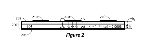
[0021] Figure 2 illustrates an embodiment of the dielectric for a
transmission apparatus.
[0022] Figure 3 illustrates yet another embodiment of the transmission
apparatus.
[0023] Figures 4A and 4B illustrate an embodiment for a software controlled
antenna
utilizing the disclosed dielectric sandwich.
[0024] Figure 5 illustrates an embodiment for a non ¨radiating electronic
device utilizing the
disclosed dielectric sandwich.
[0025] Figure 6 illustrates a variant embodiment for an RF transmission
conduit.
DETALIED DESCRIPTION
[0026] Embodiments of the inventive dielectric sandwich will now be
described with
reference to the drawings. Different embodiments or their combinations may be
used for
different applications or to achieve different benefits. Depending on the
outcome sought to be
achieved, different features disclosed herein may be utilized partially or to
their fullest, alone or
in combination with other features, balancing advantages with requirements and
constraints.
Therefore, certain benefits will be highlighted with reference to different
embodiments, but are
not limited to the disclosed embodiments. That is, the features disclosed
herein are not limited to
the embodiment within which they are described, but may be "mixed and matched"
with other
features and incorporated in other embodiments.
[0027] Figure 1 illustrates a cross-section of a prior art device that
utilizes Teflon as the
dielectric material 100. In this example, the dielectric constant of the
Teflon is Er = 2.2, while its
loss factor (loss tangent - Ohmic losses) is tg6 = 0.0009. A ground conductor
105 is provided on
the bottom of the dielectric 100, and a conducting and/or radiating electrode
110, such as a
microstrip, is provided on top of the dielectric 100. The thickness of the
dielectric is indicated as
h.
[0028] The open-head arrows in Figure 1 illustrate the resulting field. As
illustrated in
Figure 1, part of the field travels only through the dielectric material, but
some part of the field
travels through both air and the dielectric material. Therefore, the effective
dielectric constant is
some average of the dielectric constant of the air and the dielectric constant
of the Teflon (or
other dielectric material used). The effective dielectric constant correlates
to the square root of
CA 03101948 2020-10-27
WO 2019/212542 PCT/US2018/030529
the product of the two dielectric constants, weighted by the effective volume.
Since in the
drawing of Figure 1 the dielectric constant of air is 1, the effective
dielectric constant of the
structure of Figure 1 equals that of the Teflon.
[0029] Figure 2 illustrates a general embodiment utilizing the innovative
dielectric
arrangement. In the embodiment of Figure 2, the dielectric sandwich 200 is
made up of two
materials: a plate 202 having high dielectric constant, e.g.,
Polytetrafluoroethylene, Polyethylene
terephthalate (PET), glass fiber impregnated Polypropylene, or glass plate,
and a plate of
material having dielectric constant close to that of air, for example a
structural foam that is
mostly air, like, e.g., Rohacell 204. The ratio of the thicknesses of the two
plates, hl/h2, is
calculated to achieve the desired effective dielectric constant. For example,
in the embodiment
of Figure 2, a Vycor glass may be used. Vycor glass is a high silica glass
marketed by
Corning, and has a very low thermal coefficient of expansion. Depending on the
formula used
for fabrication, Vycor glass can have a dielectric constant of 3.8-4.4, with
loss factor of 0.0003.
The plate 204, made of Rohacell, has a dielectric constant of about 1.06 and
loss factor of
0.0003. Thus, in this example, when making the thicknesses of both plates the
same, i.e., hl/h2
= 1, the effective dielectric constant is Er = 2.159, while the effective loss
factor (serially
additive) is tg6 = 0.0009.
[0030] From the example of Figure 2, it can be seen that disclosed
embodiments provide a
dielectric consisting of multiple layers of insulating materials contiguous
with each other,
thereby creating a low loss dielectric that may be tailored to have an
effective dielectric similar
to Teflon. The top layer in one example is made of a plate of glass. In Figure
2 an array of three
radiating elements 210 are shown, although for clarity the field lines of only
one radiating
element 210 are shown.
[0031] Figure 3 illustrates a cross-section of another embodiment utilizing
a multiple layers
dielectric approach. The dielectric sandwich 300 of the embodiment of Figure 3
is made up of
three layers: a first glass plate 302, a second glass plate 303, and a space
306 that is filled with
air. The plates 302 and 303 are held apart with exact separation h2 using the
spacers 308. The
ground plate is formed on the bottom face of glass 303, while the transmission
line or radiating
electrode are formed on the top surface of glass 302. The thicknesses, hl and
h3, of glass plate
302 and glass plate 303, respectively, are calculated to provide the desired
effective dielectric
6
CA 03101948 2020-10-27
WO 2019/212542 PCT/US2018/030529
constant, once calculated with the layer 306 of air in between. In this case,
if one makes hl + h3
= h2, i.e., the thickness of the top glass plate plus the thickness of the
bottom glass plate equals
the air separation, then the effective dielectric constant is 2.09.
[0032] Thus, the embodiment of Figure 3 provides a dielectric plate made
out of two plates
separated using spacers to form air gap in between the two plates. Each of the
plate may be
made of glass, such as Vycor glass. Additionally, the spacers may also be made
of Vycor glass.
A ground plate may be formed on one glass, while the conductive line of
radiating patch may be
formed on the other glass plate.
[0033] Thus, as can be understood, according to one aspect, a radiating
device is
provided, comprising: a dielectric plate; a conductive ground plane formed on
bottom surface
of the dielectric plate; and a radiating element formed on top surface of the
dielectric plate;
wherein the dielectric plate comprises a plate of glass and a plate of foam.
[0034] An example of a radiating device made using the innovative
dielectric sandwich is
shown in Figures 4A-4B. In United States Patent Application No. 15/654,643,
Applicant
disclosed a multi-layered software defined antenna which utilizes an array of
radiating devices
similar to that of Figures 4A-4B, thus only relevant parts relating to one of
the radiating elements
will be repeated herein. Figure 4B is a cross-section of the device shown in
top view in Figure
4A, which is one example showing a multi-layered software defined antenna
constructed using
the dielectric sandwich disclosed herein.
[0035] The radiating patch is indicated as patch 410 and the delay line is
indicated as
conductive line 415. The radiating patch is formed on a top dielectric spacer
400 is generally
in the form of a dielectric (insulating) plate or a dielectric sheet, but in
this embodiment is
made of a dielectric sandwich consisting of glass plate 402 and foam plate
404, e.g., Rohacell.
The radiating patch 410 is formed on the top surface of the glass by, e.g.,
adhering a
conductive film, sputtering, printing, etc. At the patch location, a via 425
is formed in the
glass 402 and foam 404, and a conductor is passed through the via and is
connected to the
back surface of the patch 410. A delay line 415 is formed on the bottom
surface of foam plate
404 (or on top surface of upper binder 442), and is connected physically and
electrically to
conductor in via 425. That is, there is a continuous DC electrical connection
from the delay
line 415 to radiating patch 410, through contact in via 425. As shown in
Figure 4A, the delay
7
CA 03101948 2020-10-27
WO 2019/212542
PCT/US2018/030529
line 415 is a meandering conductive line and may take on any shape so as to
have sufficient
length to generate the desired delay, thereby causing the desired phase shift
in the RF signal.
[0036] The delay in the delay line 415 is controlled by the variable
dielectric constant
(VDC) plate 440 having variable dielectric constant material 444. While any
manner for
constructing the VDC plate 440 may be suitable for use with the embodiments of
the antenna,
as a shorthand in the specific embodiments the VDC plate 440 is shown
consisting of upper
binder 442, (e.g., glass, PET, etc.) variable dielectric constant material 444
(e.g., twisted
nematic liquid crystal layer), and bottom binder 446. In other embodiments one
or both of the
binder layers 442 and 444 may be omitted. Alternatively, adhesive such as
epoxy or glass
beads may be used instead of the binder layers 442 and/or 444. Also, as
illustrated in Figure
4B, one or both of the binders may be constructed as a sandwich according to
the
embodiments disclosed herein. As an example, bottom binder 446 is shown as a
two layer
sandwich having a foam plate 448 and a glass plate 449.
[0037] In some embodiments, e.g., when using twisted nematic liquid crystal
layer, the
VDC plate 440 also includes an alignment layer that may be deposited and/or
glued onto the
bottom of the upper binder 442. The alignment layer may be a thin layer of
material, such as
polyimide-based PVA, that is being rubbed or cured with UV radiation in order
to align the
molecules of the LC at the edges of confining substrates.
[0038] The effective dielectric constant of VDC plate 440 can be controlled
by applying
DC potential across the VDC plate 440. For that purpose, electrodes are formed
and are
connected to controllable voltage potential. There are various arrangements to
form the
electrodes, and several examples will be shown in the disclosed embodiments.
In the
arrangement shown in Figure 4B, two electrodes 443 and 447 and provided ¨ one
on the
bottom surface of the upper binder 442 and one on the upper surface of the
bottom binder
446. As one example, electrode 447 is shown connected to variable voltage
potential 441,
while electrode 443 is connected to ground. As one alternative, shown in
broken line,
electrode 443 may also be connected to a variable potential 439.
[0039] Thus, by changing the output voltage of variable potential 441
and/or variable
potential 439, one can change the dielectric constant of the VDC material in
the vicinity of the
electrodes 443 and 447, and thereby change the RF signal traveling over delay
line 415.
8
CA 03101948 2020-10-27
WO 2019/212542
PCT/US2018/030529
Changing the output voltage of variable potential 441 and/or variable
potential 439 can be
done using a controller, Ctl, running software that causes the controller to
output the
appropriate control signal to set the appropriate output voltage of variable
potential 441 and/or
variable potential 439. Similarly, a conventional controller can be used to
provide the control
and common signals to control the characteristics of the antenna. Thus, the
antenna's
performance and characteristics can be controlled using software ¨ hence
software controlled
antenna.
[0040] At this point it should be clarified that in the subject description
the use of the term
ground refers to both the generally acceptable ground potential, i.e., earth
potential, and also
to a common or reference potential, which may be a set potential or a floating
potential. For
example, conventional LCD display controllers output two signals per pixel,
one of which is
referred to as the ground or common signal. Similarly, while in the drawings
the symbol for
ground is used, it is used as shorthand to signify either an earth or a common
potential,
interchangeably. Thus, whenever the term ground is used herein, the term
common or
reference potential, which may be set or floating potential, is included
therein.
[0041] In transmission mode the RF signal is applied to the feed patch 460
via connector
465 (e.g., a coaxial cable connector). As shown in Figure 4B, there is no
electrical DC
connection between the feed patch 460 and the delay line 415. However, in
disclosed
embodiments the layers are designed such that an RF short is provided between
the feed patch
460 and delay line 415. As illustrated in Figure 4B, a back plane conductive
ground (or
common) 455 is formed on the top surface of backplane insulator (or
dielectric) 450 or the
bottom surface of bottom binder 446. The back plane conductive ground 455 is
generally a
layer of conductor covering the entire area of the antenna array. At each RF
feed location a
window (DC break) 453 is provided in the back plane conductive ground 455. The
RF signal
travels from the feed patch 460, via the window 453, and is coupled to the
delay line 415.
The reverse happens during reception. Thus, a DC open and an RF short are
formed between
delay line 415 and feed patch 460. The backplane insulator 450 can also be
constructed
according to embodiments disclosed herein, which in this example includes
glass plate 452,
foam plate 454, and glass plate 456.
9
CA 03101948 2020-10-27
WO 2019/212542 PCT/US2018/030529
[0042] Thus, as can be understood, according to one aspect, a radiating
device is
provided, comprising: a dielectric plate; a radiating element formed on top
surface of the
dielectric plate; a dielectric back-plate; a conductive ground plane formed on
bottom surface
of the dielectric back-plate; a variable dielectric constant material
sandwiched between the
dielectric plate and the dielectric back-plate; and wherein at least one of
the dielectric plate
and dielectric back-plate comprises a plate of glass and a plate of foam.
[0043] As illustrated so far, the embodiments disclosed herein can be used
for radiating
elements, such as antennas and antenna arrays. However, according to aspects
of the invention,
electronic devices or components can also be provided, which have variable
electrical
characteristics or operation based on potential applied to a variable-
dielectric constant sector
associated with the device and incorporate the low-cost dielectric sandwich.
According to
aspects of the invention, the electronic devices or component may include
bends, power splitters,
filters, ports, phase shifters, frequency shifters, attenuators, couplers,
capacitors, inductors,
diplexers, hybrids of beam forming networks, and may also include radiating
elements in
addition to the electronic devices. Notably, several devices can be formed on
the same dielectric
sandwich, just like was done in the prior art using Rogers or PCP.
[0044] According to disclosed aspects, the electronic devices disclosed in
Applicant's U.S.
Patent Application, Ser. No. can be modified using the sandwich dielectric
plate, to thereby
provide the same performance, at a much lower cost. Figure 5 illustrates an
embodiment of a
four-ports hybrid coupler 500. Without any VDC's the signal input at port 1
splits into output to
port 2 without phase change and into port 3 at 90 degrees phase change.
Similarly, a signal input
to port 4 splits into output to port 3 without phase change and into port 2 at
90 degrees phase
change. This is captured by the table shown in Figure 5. However, in the
embodiment of Figure
several optional placement for VDC's are shown, all or some of which may be
implemented,
depending on the desired control over the operation of the hybrid coupler 500.
[0045] For example, VDC 503 is provided under the line of input port 1. By
applying
voltage potential to the electrodes of VDC 503, the phase of the input signal
can be controlled.
Consequently, the phase at both output ports 2 and 3 would be varied together
based on the phase
change caused by the voltage potential at VDC 503. This means that the phase
at output 2 can be
different from the phase of the input signal at input port 1. On the other
hand, the phase at output
CA 03101948 2020-10-27
WO 2019/212542 PCT/US2018/030529
2 can be changed independently by voltage potential at VDC 507. Consequently,
the phase at
output port 3 would remain 90 from the input at input port 1, but the phase
at output port 2
would be different from zero, depending on the voltage potential applied to
VDC 507.
Additionally, a voltage potential can be applied to the electrodes of VDC 527
to vary the phase at
output port 3 independent of the output at port 2. Thus, the output at port 2
can remain at the
same phase as the input at port 1, but the output at port 3 can be modified
from 90 with respect
to the input at port 1. The same effect can be applied to the input of input
port 4 by applying
voltage potential to VDC's 523, 507 and 527. Moreover, normally an input
signal at port 1
would be split at equal energies between output ports 2 and 3. However, by
controlling the
voltage potential at VDCs 508, 528, 515A and 515B, the amount of energy
delivered to each
output port can be changed, thus the amplitude of the output at each port can
be controlled.
[0046] The cross-section structure of the device shown in Figure 5 can be
seen in the
callout of Figure 5. Element 527 is the variable dielectric constant material,
that receive
potential from power supplier V. The conductive line 520 is formed on top of a
dielectric
plate 550, that may be made according to any of the embodiments disclosed
herein. For
example, it may be made of a sandwich of glass plate and foam plate. The same
goes for the
back-plate 555, it also may be made according to any of the embodiments
disclosed herein.
For example, it may be made of a sandwich of glass plate and foam plate.
[0047] Thus, as can be understood, according to one aspect, an electronic
device is provided,
comprising: a back-plate; a dielectric plate; a variable dielectric constant
material sandwiched
between the back-plate and the dielectric plate; electrodes configured for
applying electrical
potential to the variable dielectric constant material; and a conductive line
formed on top of the
dielectric plate; wherein at least one of the dielectric plate and the back-
plate comprises a plate of
glass and a plate of foam.
[0048] Figure 6 illustrates a variant embodiment for an RF transmission
conduit, which may
be radiating, non-radiating, or both, e.g., a non-radiating transmission line
leading to a radiating
patch. In the embodiment of Figure 6, the dielectric sandwich 200 is made up
of two materials: a
top layer of PET (Polyethylene terephthalate) 607 having high dielectric
constant, a plate of
material having dielectric constant close to that of air, for example a
structural foam 604 that is
mostly air, like, e.g., Rohacell, and a bottom layer of PET 608. The ratio of
the thicknesses of
11
CA 03101948 2020-10-27
WO 2019/212542 PCT/US2018/030529
the two PET layers and the foam plate, (hl+h3)/h2, is calculated to achieve
the desired effective
dielectric constant. For example, in the example of Figure 6, a PET layer
having dielectric
constant of about 4.0 at 3GHz is used. Depending on the formula used for
fabrication of the
PET, it may have a somewhat different dielectric constant, but it is within
the range of 3.8-4.4.
[0049] In the example of Figure 2, a conductive line or patch 610 is
fabricated on the top
surface of PET 607. A conductive ground plane 605 is fabricated on the bottom
surface of PET
608. Then the PET payers are adhered to the foam core 604. This makes it very
easy to
fabricate, since the conductive line 610 and conductive ground plane 605 are
very easy to
fabricate over PET, using various techniques, such as printing, sputtering,
plating, etc.
Moreover, the conductive circuitry 610 and 605 can be easily fabricated over
the PET using reel-
to-reel methods, which is fast and economical.
[0050] As with all RF antennas, reception and transmission are symmetrical,
such that a
description of one equally applies to the other. In this description it may be
easier to explain
transmission, but reception would be the same, just in the opposite direction.
[0051] It should be understood that processes and techniques described
herein are not
inherently related to any particular apparatus and may be implemented by any
suitable
combination of components. Further, various types of general purpose devices
may be used in
accordance with the teachings described herein. The present invention has been
described in
relation to particular examples, which are intended in all respects to be
illustrative rather than
restrictive. Those skilled in the art will appreciate that many different
combinations will be
suitable for practicing the present invention.
[0052] Moreover, other implementations of the invention will be apparent to
those skilled in
the art from consideration of the specification and practice of the invention
disclosed herein.
Various aspects and/or components of the described embodiments may be used
singly or in any
combination. It is intended that the specification and examples be considered
as exemplary only,
with a true scope and spirit of the invention being indicated by the following
claims.
12