Note: Descriptions are shown in the official language in which they were submitted.
CA 03103940 2020-12-15
WO 2019/246010 PCT/US2019/037603
APPARATUSES INCLUDING A CAPACITIVE MICROMACHINED
ULTRASONIC TRANSDUCER DIRECTLY COUPLED TO AN ANALOG-
TO-DIGITAL CONVERTER
CROSS-REFERENCE TO RELATED APPLICATION
[0001] The present application is a continuation-in-part claiming the benefit
under 35 U.S.C.
120 of U.S. Application Serial No. 16/192,603, filed November 15, 2018, under
Attorney
Docket No. B1348.70065U501, and entitled "ULTRASOUND APPARATUSES AND
METHODS FOR FABRICATING ULTRASOUND DEVICES," which claims the benefit under
35 U.S.C. 119(e) of U.S. Provisional Application Serial No. 62/586,716, filed
November 15,
2017, under Attorney Docket No. B1348.70065U500, and entitled "METHODS AND
APPARATUS FOR IMPLEMENTING INTEGRATED TRANSMIT AND RECEIVE
CIRCUITRY IN AN ULTRASOUND DEVICE," each of which is hereby incorporated
herein
by reference in their entirety.
[0002] The present application is also an application claiming the benefit
under 35 U.S.C.
119(e) of U.S. Provisional Application Serial No. 62/687,189, filed June 19,
2018, under
Attorney Docket No. B1348.70083U500, and entitled "APPARATUSES INCLUDING A
CAPACITIVE MICROMACHINED ULTRASONIC TRANSDUCER DIRECTLY COUPLED
TO AN ANALOG-TO-DIGITAL CONVERTER", which is hereby incorporated herein by
reference in its entirety.
FIELD
[0003] Generally, the aspects of the technology described herein relate to
ultrasound apparatuses.
Some aspects relate to ultrasound apparatuses including a capacitive
micromachined ultrasonic
transducer (CMUT) directly coupled to a delta-sigma analog-to-digital
converter (ADC).
BACKGROUND
[0004] Ultrasound devices may be used to perform diagnostic imaging and/or
treatment, using
sound waves with frequencies that are higher with respect to those audible to
humans.
Ultrasound imaging may be used to see internal soft tissue body structures,
for example to find a
-1-
CA 03103940 2020-12-15
WO 2019/246010 PCT/US2019/037603
source of disease or to exclude any pathology. When pulses of ultrasound are
transmitted into
tissue (e.g., by using a probe), sound waves are reflected off the tissue,
with different tissues
reflecting varying degrees of sound. These reflected sound waves may then be
recorded and
displayed as an ultrasound image to the operator. The strength (amplitude) of
the sound signal
and the time it takes for the wave to travel through the body provide
information used to produce
the ultrasound image. Many different types of images can be formed using
ultrasound devices,
including real-time images. For example, images can be generated that show two-
dimensional
cross-sections of tissue, blood flow, motion of tissue over time, the location
of blood, the
presence of specific molecules, the stiffness of tissue, or the anatomy of a
three-dimensional
region.
SUMMARY
[0005] According to one aspect, an apparatus includes a capacitive
micromachined ultrasonic
transducer (CMUT) directly electrically coupled to a delta-sigma analog-to-
digital converter
(ADC). According to another aspect, an apparatus includes a capacitive
micromachined
ultrasonic transducer (CMUT) electrically coupled to a delta-sigma analog-to-
digital converter
(ADC), wherein the apparatus lacks an amplifier or a multiplexer between the
CMUT and the
delta-sigma ADC.
[0006] In some embodiments of these aspects, the apparatus includes between
100-1,000
CMUTs and between 100-1,000 delta-sigma ADCs, each of the CMUTs directly
electrically
coupled to one of the delta-sigma ADCs. In some embodiments of these aspects,
the apparatus
includes between 1,000-10,000 CMUTs and between 1,000-10,000 delta-sigma ADCs,
each of
the CMUTs directly electrically coupled to one of the delta-sigma ADCs. In
some embodiments
of these aspects, the apparatus includes between 10,000-20,000 CMUTs and
between 10,000-
20,000 delta-sigma ADCs, each of the CMUTs directly electrically coupled to
one of the delta-
sigma ADCs. In some embodiments of these aspects, the CMUTs and the delta-
sigma ADCs are
monolithically integrated on a single substrate. In some embodiments of these
aspects, the delta-
sigma ADC lacks an integrator distinct from the CMUT. In some embodiments of
these aspects,
an internal capacitance of the CMUT serves as an integrator for the delta-
sigma ADC.
[0007] According to another aspect, an apparatus includes between 100-20,000
CMUTs; and one
-2-
CA 03103940 2020-12-15
WO 2019/246010 PCT/US2019/037603
ADC dedicated for each of the CMUTs.
[0008] In some embodiments, the apparatus includes between 100-1,000 CMUTs. In
some
embodiments, the apparatus includes between 1,000-10,000 CMUTs. In some
embodiments, the
apparatus includes between 10,000-20,000 CMUTs. In some embodiments, the CMUTs
and the
ADCs are monolithically integrated on a single substrate.
[0009] According to another aspect, an apparatus includes a CMUT having an
output terminal; a
quantizer having an input terminal and an output terminal; and a current
digital-to-analog
converter (DAC) having an input terminal and an output terminal; wherein the
output terminal of
the CMUT is electrically coupled to the input terminal of the quantizer; the
output terminal of the
quantizer is electrically coupled to the input terminal of the current DAC;
and the output terminal
of the current DAC is electrically coupled to the input terminal of the
quantizer.
[0010] In some embodiments, the quantizer is a 1.5-bit quantizer. In some
embodiments, the
output terminal of the CMUT is directly electrically coupled to the input
terminal of the
quantizer. In some embodiments, the apparatus lacks an integrator between the
output terminal
of the CMUT and the input terminal of the quantizer. In some embodiments, the
apparatus lacks
an integrator between the output terminal of the current DAC and the input
terminal of the
quantizer.
[0011] According to another aspect, an apparatus includes a CMUT having an
output terminal; a
transconductance amplifier having an input terminal and an output terminal; a
capacitor; a
quantizer having an input terminal and an output terminal; a first current
digital-to-analog
converter (DAC) having an input terminal and an output terminal; and a second
current digital-
to-analog converter (DAC) having an input terminal and an output terminal;
wherein the output
terminal of the CMUT is electrically coupled to the input terminal of the
transconductance
amplifier; the output terminal of the transconductance amplifier is
electrically coupled to the
input terminal of the quantizer; the output terminal of the quantizer is
electrically coupled to the
input terminal of the first current DAC and the second current DAC; the output
terminal of the
first current DAC is electrically coupled to the input terminal of the
transconductance amplifier;
the output terminal of the second current DAC is electrically coupled to the
output terminal of
the transconductance amplifier; and the capacitor is electrically coupled
between the output
terminal of the transconductance amplifier; and a DC voltage.
-3-
CA 03103940 2020-12-15
WO 2019/246010 PCT/US2019/037603
[0012] In some embodiments, the quantizer is a 1.5-bit quantizer. In some
embodiments, the
output terminal of the CMUT is directly electrically coupled to the input
terminal of the
quantizer. In some embodiments, the apparatus lacks an integrator between the
output terminal
of the CMUT and the input terminal of the quantizer. In some embodiments, the
apparatus lacks
an integrator between the output terminal of the first current DAC and the
input terminal of the
quantizer.
[0013] According to another aspect, an apparatus includes a CMUT having an
output terminal; a
transconductance amplifier having an input terminal and an output terminal; a
capacitor; a
quantizer having an input terminal and an output terminal; a current digital-
to-analog converter
(DAC) having an input terminal and an output terminal; a voltage buffer having
an input
terminal and an output terminal; and a voltage adder having a first input
terminal, a second input
terminal, and an output terminal; wherein the output terminal of the CMUT is
electrically
coupled to the input terminal of the transconductance amplifier; the output
terminal of the
transconductance amplifier is electrically coupled to the first input terminal
of the voltage adder;
the input terminal of the voltage buffer is electrically coupled to the input
terminal of the
transconductance amplifier; the output terminal of the voltage buffer is
electrically coupled to the
second input terminal of the voltage adder; the output terminal of the voltage
adder is electrically
coupled to the input terminal of the quantizer; the output terminal of the
quantizer is electrically
coupled to the input terminal of the first current DAC; the output terminal of
the current DAC is
electrically coupled to the input terminal of the transconductance amplifier;
and the capacitor is
electrically coupled between the output terminal of the transconductance
amplifier and a DC
voltage.
[0014] In some embodiments, the quantizer is a 1.5-bit quantizer. In some
embodiments, the
output terminal of the CMUT is directly electrically coupled to the input
terminal of the
quantizer. In some embodiments, the apparatus lacks an integrator between the
output terminal
of the CMUT and the input terminal of the quantizer. In some embodiments, the
apparatus lacks
an integrator between the output terminal of the current DAC and the input
terminal of the
quantizer.
BRIEF DESCRIPTION OF THE DRAWINGS
-4-
CA 03103940 2020-12-15
WO 2019/246010 PCT/US2019/037603
[0015] Various aspects and embodiments will be described with reference to the
following
exemplary and non-limiting figures. It should be appreciated that the figures
are not necessarily
drawn to scale. Items appearing in multiple figures are indicated by the same
or a similar
reference number in all the figures in which they appear.
[0016] FIG. 1 illustrates an example circuit model of a capacitive
micromachined ultrasonic
transducer (CMUT);
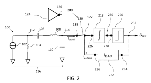
[0017] FIG. 2 illustrates a diagram of a CMUT electrically coupled to a delta-
sigma analog-to-
digital converter (ADC);
[0018] FIG. 3 illustrates a diagram of a CMUT electrically coupled to another
delta-sigma ADC,
in accordance with certain embodiments;
[0019] FIG. 4 illustrates a diagram of a CMUT electrically coupled to another
delta-sigma ADC,
in accordance with certain embodiments;
[0020] FIG. 5 illustrates a diagram of a CMUT electrically coupled to another
delta-sigma ADC,
in accordance with certain embodiments;
[0021] FIG. 6 illustrates a diagram of a CMUT electrically coupled to another
delta-sigma ADC,
in accordance with certain embodiments;
[0022] FIG. 7 illustrates a diagram of a CMUT electrically coupled to another
delta-sigma ADC,
in accordance with certain embodiments;
[0023] FIG. 8 illustrates a diagram of a CMUT electrically coupled to another
delta-sigma ADC,
and the delta-sigma ADC electrically coupled to a filter and a dither
generator, in accordance
with certain embodiments;
[0024] FIG. 9 illustrates a diagram of the first current digital-to-analog
(DAC) converter of FIG.
8 and its coupling to the transconductance amplifier of FIG. 8;
[0025] FIG. 10 illustrates a diagram of the second current DAC of FIG. 8 and
its coupling to the
transconductance amplifier and capacitors of FIG. 8, in accordance with
certain embodiments;
[0026] FIG. 11 illustrates an example circuit implementation of a current
source of FIG. 10, in
accordance with certain embodiments;
[0027] FIG. 12 illustrates an example circuit implementation of another
current source of FIG.
10, in accordance with certain embodiments;
[0028] FIG. 13 illustrates an example diagram of the dither generator of FIG.
8, in accordance
-5-
CA 03103940 2020-12-15
WO 2019/246010 PCT/US2019/037603
with certain embodiments; and
[0029] FIG. 14 illustrates an example diagram of an ultrasound system
including CMUTs,
ADCs, filters, and a digital beamformer, in accordance with certain
embodiments.
DETAILED DESCRIPTION
[0030] Conventional ultrasound systems are large, complex, and expensive
systems that are
typically only purchased by large medical facilities with significant
financial resources.
Recently, cheaper and less complex ultrasound imaging devices have been
introduced. Such
imaging devices may include capacitive micromachined ultrasonic transducers
(CMUTs)
monolithically integrated onto a single semiconductor die to form a monolithic
ultrasound
device. Aspects of such ultrasound-on-a chip devices are described in U.S.
Patent Application
No. 15/415,434 titled "UNIVERSAL ULTRASOUND DEVICE AND RELATED
APPARATUS AND METHODS," filed on January 25, 2017, which is incorporated by
reference
herein in its entirety.
[0031] In some ultrasound systems, an ultrasonic signal received from a single
ultrasonic
transducer element, which is typically an analog current signal, is converted
to an analog voltage
signal by a per-element transimpedance amplifier (where per-element means one
per ultrasonic
transducer element in the ultrasound system). The analog voltage signal is
then processed
further by a per-element time-gain compensation amplifier, which compensates
for attenuation of
the ultrasonic signal in the tissue of the subject being imaged. The
transimpedance amplifier and
the time-gain compensation amplifiers, which are analog amplifiers, may
consume substantial
power. After this analog amplification, it may not be practical to implement a
per-element
analog-to-digital converter (ADC), as this may exceed the power budget in
combination with the
power consumed by the analog amplifiers. Accordingly, to reduce the number of
individual
analog signals that must be digitized, analog beamforming is performed on the
per-element
analog signals. The analog outputs of the analog beamformers, which are fewer
in number than
the number of ultrasonic transducer elements, are then digitized by ADCs.
However, analog
beamforming suffers from low signal-to-noise ratio (SNR), low sampling
resolution, inflexibility
in delay patterns implemented by the analog beamformer, and inflexibility in
grouping of
ultrasonic transducers for processing by the analog beamformer.
-6-
CA 03103940 2020-12-15
WO 2019/246010 PCT/US2019/037603
[0032] Digital beamforming, in which beamforming is performed on per-element
digital signals,
may provide higher SNR, higher sampling resolution, more flexibility in delay
patterns
implemented by the digital beamformer, and more flexibility in grouping of
ultrasonic
transducers for processing by the digital beamformers. However, digital
beamforming requires
that the analog ultrasonic signal received from each ultrasonic transducer
element be individually
digitized by per-element ADCs. Implementing and operating per-element ADCs
presents
challenges including power consumption by the ADCs and the area in an
integrated circuit
required by the per-element ADCs.
[0033] The inventors have recognized that a delta-sigma ADC (also sometimes
referred to as a
sigma-delta ADC) may enable per-element digitization while not being
impractical in terms of
power and area. In particular, in some embodiments, each CMUT of an ultrasound
system is
directly electrically coupled to a per-element delta-sigma ADC. Directly
electrically coupling a
CMUT to a delta-sigma ADC may mean that there are no amplifiers or
multiplexers between the
CMUT and the delta-sigma ADC. The inventors have further recognized that
parasitic
capacitance inherent to a CMUT may provide integration capability for the
delta-sigma ADC
that is typically provided by a separate integrator component. Obviating the
need for a separate
integrator component may further reduce power consumption and area.
[0034] A CMUT being directly electrically coupled to a delta-sigma ADC should
not be
understood to exclude the CMUT being electrically coupled to the delta-sigma
ADC through a
switch that is electrically coupled between the CMUT and the delta-sigma ADC.
More
generally, electrically coupling and directly electrically coupling two
components together
should not be understood to exclude a switch being electrically coupled
between the two
components.
[0035] According to aspects of the present application, an ultrasonic
transducer configured to
produce an analog output signal is coupled to downstream processing circuitry
which operates
only in a digital domain. For instance, in some embodiments, an ultrasonic
transducer is coupled
to an ADC without intervening analog signal processing circuitry (including
analog signal
conditioning circuitry). In some embodiments, the ultrasonic transducer is
coupled to an ADC
without intervening analog amplifiers, multiplexers, filters, or other signal
conditioning
circuitry. A switch may couple the ultrasonic transducer to the ADC, but the
switch itself may
-7-
CA 03103940 2020-12-15
WO 2019/246010 PCT/US2019/037603
not perform signal processing or conditioning. In some embodiments, the
ultrasonic transducer
is coupled to an ADC without intervening active circuitry, or without
intervening active circuitry
other than a switch used to couple the ultrasonic transducer to the ADC. In
some embodiments,
the ultrasonic transducer is coupled to an ADC without intervening active
analog circuitry. In
some embodiments, an ADC is directly digitally coupled to an output of an
ultrasonic transducer,
without intervening analog signal processing or conditioning circuitry. In
some embodiments, an
ultrasonic transducer may be said be directly digitally coupled when its
output is coupled to
digital processing circuitry without intervening analog processing circuitry.
[0036] FIG. 1 illustrates an example circuit model of a capacitive
micromachined ultrasonic
transducer (CMUT) 100. The model of the CMUT 100 includes a current source
102, a resistor
104, a capacitor 106, an inductor 108, a capacitor 110, a node 112, an output
terminal 114, and
ground 116. The current source 102 is electrically coupled between the node
112 and ground
116. The resistor 104 is electrically coupled between the node 112 and ground
116. The
capacitor 106 and the inductor 108 are electrically coupled in series and are
electrically coupled
between the node 112 and the output terminal 114. The capacitor 110 is
electrically coupled
between the output terminal 114 and ground 116. The current source 102 may
model the current
signal generated by the CMUT 100 in response to ultrasonic waves. The resistor
104, the
capacitor 106, and the inductor 108 may model the resonant property of the
CMUT 100. The
capacitor 110 may model parasitic capacitance of the CMUT 100. The current
difference, ICMUT,
between the current entering the output terminal 114 and exiting the output
terminal 114 through
the capacitor 110 may be considered the output current of the CMUT 100.
[0037] The resonator formed by the resistor 104, the capacitor 106, and the
inductor 108 may be
considered a low-Q resonator in that the Q of the resonator may be less than
0.5. The resistance
of the resistor 104 may be significantly greater than 1/(co*Cp), where co is
the frequency of the
current signal ICMUT and Cp is the capacitance of the capacitor 110. In some
embodiments, Cp
may be on the order of tenths of femtofarads to tens of millifarads. In some
embodiments, ICMUT
may be on the order of tens of picoamps to hundreds of microamps, including
any value in those
ranges.
[0038] In some embodiments, the capacitance of the capacitor 110 dominates the
behavior of the
CMUT 100. Furthermore, as will be described below, the capacitor 110 may be
used to provide
-8-
CA 03103940 2020-12-15
WO 2019/246010 PCT/US2019/037603
integration functionality for a delta-sigma ADC to which the CMUT 100 is
electrically coupled.
This may obviate the need for a separate integrator in the delta-sigma ADC. In
contrast, in
circuit models of piezoelectric ultrasonic transducers, elements of the
piezoelectric ultrasonic
transducer forming a resonator may dominate parasitic capacitance elements.
Therefore,
parasitic capacitance within a piezoelectric ultrasonic transducer may not be
able to be used for
integration functionality in a delta-sigma ADC. Furthermore, the resonant
elements of the
piezoelectric ultrasonic transducer may be undesirable and require
implementation of extra
circuit elements to compensate for resonant behavior.
[0039] FIG. 2 illustrates a diagram of the CMUT 100 (as represented by the
circuit model of
CMUT 100 described with reference to FIG. 1) electrically coupled to a delta-
sigma analog-to-
digital converter (ADC) 200, in accordance with certain embodiments. FIG. 2
further shows a
pulser 124 and a switch 120. The delta-sigma ADC 200 includes a current
integrator 218, a
voltage quantizer 220, and a current digital-to-analog converter (current DAC
or IoAc) 222. The
current integrator 218 includes an input terminal 226 and an output terminal
230. The voltage
quantizer 220 includes an input terminal 228 and an output terminal 232. The
current DAC 222
includes an input terminal 234 and an output terminal 236. The switch 120
includes an input
terminal 118 and an output terminal 122. The pulser 124 includes an output
terminal 126. (The
input terminal of the pulser 124, which may be electrically coupled to other
circuitry, is not
shown in FIG. 2.) The output terminal 126 of the pulser 124 is electrically
coupled to the output
terminal 114 of the CMUT 100. The input terminal 118 of the switch 120 is
electrically coupled
to the output terminal 114 of the CMUT 100. The output terminal 236 of the
current DAC 222 is
electrically coupled to the output terminal 122 of the switch 120. The input
terminal of the 226
of the current integrator 218 is electrically coupled to the output terminal
122 of the switch 120.
The output terminal 230 of the current integrator 218 is electrically coupled
to the input terminal
228 of the quantizer. The output terminal 232 of the voltage quantizer 220 is
electrically coupled
to the input terminal 234 of the current DAC 222. The output terminal 236 of
the current DAC
222 is electrically coupled to the output terminal 122 of the switch 100.
[0040] In operation, in transmit mode, the switch 120 may be configured to
open (i.e., the input
terminal 118 of the switch 120 is electrically disconnected from the output
terminal 122 of the
switch 120), thus disconnecting the CMUT 100 from the delta-sigma ADC 200. The
pulser 124
-9-
CA 03103940 2020-12-15
WO 2019/246010 PCT/US2019/037603
may be configured to output a driving signal to the CMUT 100 for generating
and transmitting
an ultrasound signal based on the driving signal. Because the CMUT 100 is
disconnected from
the delta-sigma ADC 200, the delta-sigma ADC 200 may not interfere with the
driving signal. In
receive mode, the switch 120 may be configured to close (i.e., the input
terminal 118 of the
switch 120 may be electrically connected to the output terminal 122 of the
switch 120), thus
connecting the CMUT 100 to the delta-sigma ADC 200. FIG. 2 shows the switch
120 in receive
mode. In this mode, the current ICMUT may flow from the output terminal 114 of
the CMUT 100,
through the closed switch 120, and into the input terminal 226 of the
quantizer 218, and may be
considered the input to the delta-sigma ADC 200. In other words, the current
ICMUT may be the
signal that the delta-sigma ADC 200 converts from analog to digital. The
voltage DOuT at the
output terminal 232 of the voltage quantizer 220 may be considered the output
of the delta-sigma
ADC 200 and may be a digital representation of the analog signal ICMUT.
[0041] The delta-sigma ADC 200 includes a feedback loop where the current
integrator 218 and
the voltage quantizer 220 are in the forward path of the feedback loop and the
current DAC 222
is in the feedback path of the feedback loop. In operation, the current
integrator 218 may be
configured to integrate ICMUT to produce an output voltage. The quantizer 220
may be
configured to accept this output voltage as an input and outputs a digital
logic level depending on
whether the voltage is less than or greater than a threshold voltage. This
digital logic level, over
time, may be the output DOuT of the delta-sigma ADC. The current DAC 222 may
be configured
to accept the digital logic level as an input and output a corresponding
analog current 'feedback.
Through the feedback loop, 'feedback may be added to ICMUT at the output
terminal 122 of the
switch 120. This feedback loop may provide negative feedback, as in response
to a positive
input signal to the quantizer 220, the quantizer 220 may output a digital
logic level that is
converted by the current DAC 222 to a negative 'feedback, and vice versa. DOUT
may be a pulse
stream in which the frequency of pulses may be proportional to the input to
the delta-sigma ADC
200, namely the analog current signal ICMUT. This frequency may be enforced by
the feedback
loop of the delta-sigma ADC 200. As will be described further, the delta-sigma
ADC 200 may
oversample (e.g., at the quantizer 220) the processed input current signal
ICMUT, and a filter may
decimate the oversampled signal, in order to improve the signal-to-
quantization-noise ratio
(SQNR) of the delta-sigma ADC 200.
-10-
CA 03103940 2020-12-15
WO 2019/246010 PCT/US2019/037603
[0042] In some embodiments, the pulser 124 may be absent. Such embodiments may
only be
configured for receiving ultrasound signals, but not transmitting ultrasound
signals. Because
there may be no need for selecting between a transmit mode and a receive mode,
the switch 120
may also be absent.
[0043] FIG. 3 illustrates a diagram of the CMUT 100 (as represented by the
circuit model of
CMUT 100 described with reference to FIG. 1) electrically coupled to a delta-
sigma ADC 300,
in accordance with certain embodiments. The delta-sigma ADC 300 differs from
the delta-sigma
ADC 200 in that the delta-sigma ADC 300 lacks the current integrator 218. In
other words, the
output terminal 114 of the CMUT 100 is directly electrically coupled (through
the switch 120) to
the input terminal 228 of the quantizer 220. Directly electrically coupling
the output terminal
114 of the CMUT 100 to the input terminal 228 of the quantizer 220 may mean
that there is no
integrator distinct from the CMUT 100 between the output terminal 114 of the
CMUT 100 and
the input terminal 228 of the quantizer 220. The capacitor 110 of the CMUT 100
may operate as
a current integrator and replace the current integrator 218. In other words,
the CMUT 100 may
include an internal current integrator (the capacitor 110), and coupling the
CMUT 100 to the
delta-sigma ADC 300 may enable the capacitor 110 to serve as the current
integrator of the delta-
sigma ADC 300 and obviate the need for another current integrator (i.e.,
distinct from the CMUT
100) between the CMUT 100 and the voltage quantizer 220. It should be noted
that the capacitor
110 of the CMUT 100 may be considered to be within the feedback loop of the
delta-sigma ADC
300.
[0044] FIG. 4 illustrates a diagram of the CMUT 100 (as represented by the
circuit model of
CMUT 100 described with reference to FIG. 1) electrically coupled to a delta-
sigma ADC 400,
in accordance with certain embodiments. The delta-sigma ADC 400 differs from
the delta-sigma
ADC 300 in that the delta-sigma ADC 400 includes a voltage adder 438, a
voltage integrator
450, and a voltage DAC (VDAc). The voltage adder 438 includes a first input
terminal 440, a
second input terminal 456, and an output terminal 442. The voltage integrator
450 includes an
input terminal 452 and an output terminal 454. The voltage DAC 444 includes an
input terminal
446 and an output terminal 448. The first input terminal 440 of the voltage
adder 438 is
electrically coupled to the output terminal 122 of the switch 120. The second
input terminal 456
of the voltage adder 438 is electrically coupled to the output terminal 448 of
the voltage DAC
-11-
CA 03103940 2020-12-15
WO 2019/246010 PCT/US2019/037603
444. The output terminal 442 of the voltage adder 438 is electrically coupled
to the input
terminal 452 of the voltage integrator 450. The output terminal 454 of the
voltage integrator 450
is electrically coupled to the input terminal 228 of the voltage quantizer
220. The output
terminal 232 of the voltage quantizer 220 is electrically coupled to the input
terminal 446 of the
voltage DAC 444.
[0045] The delta-sigma ADC 400 includes two feedback loops. The capacitor 110,
the voltage
adder 438, the voltage integrator 450, and the voltage quantizer 220 are in
the forward path of
the first feedback loop and the current DAC 222 is in the feedback path of the
first feedback
loop. The voltage adder 438, the voltage integrator 450, and the voltage
quantizer 220 are in the
forward path of the second feedback loop and the voltage DAC 444 is in the
feedback path of the
second feedback loop. The presence of two feedback loops in the delta-sigma
ADC 400 may be
referred to as distributed feedback. The delta-sigma ADC 400 may be considered
a second-order
delta-sigma ADC in that the delta-sigma ADC 400 includes two integrators (the
capacitor 110
and the voltage integrator 450) and two feedback loops. In contrast, the delta-
sigma ADC 200
and the delta-sigma ADC 300 may be considered first-order delta-sigma ADC's in
that they
include one integrator (the current integrator 218 in the delta-sigma ADC 200
and the capacitor
110 in the delta-sigma ADC 300) and one feedback loop. A second-order delta-
sigma ADC may
provide higher signal-to-quantization-noise ratio (SQNR) compared with a first-
order delta-
sigma ADC operating at the same oversampling frequency. A second-order delta-
sigma ADC
may provide the same signal-to-quantization-noise ratio (SQNR) compared with a
first-order
delta-sigma ADC while the second-order delta-sigma ADC operates at a lower
oversampling
frequency than the first-order delta-sigma ADC.
[0046] In operation, the voltage integrator 450 may be configured to integrate
the voltage on the
capacitor 110. The integrated output of the voltage integrator 450 may be
converted to a digital
value by the voltage quantizer 220 depending on whether the integrated output
is greater than or
less than a threshold value. The voltage DAC 444 may be configured to convert
the digital
output of the voltage quantizer 220 to an analog voltage and the voltage adder
438 may be
configured to add that analog voltage to the voltage of the capacitor 110 as
negative feedback.
[0047] The delta-sigma ADC 400 may require addition of currents and addition
of voltages (by
the voltage adder 438) at the same node, the output terminal 122 of the switch
120. This may
-12-
CA 03103940 2020-12-15
WO 2019/246010 PCT/US2019/037603
make the delta-sigma ADC 400 as illustrated in FIG. 4 not practically
realizable.
[0048] FIG. 5 illustrates a diagram of the CMUT 100 (as represented by the
circuit model of
CMUT 100 described with reference to FIG. 1) electrically coupled to a delta-
sigma ADC 500,
in accordance with certain embodiments. The delta-sigma ADC 500 differs from
the delta-sigma
ADC 400 in that the delta-sigma ADC 500 includes a first voltage integrator
558 and a second
voltage integrator 562. The first voltage integrator 558 includes an input
terminal 564 and an
output terminal 566. The second voltage integrator 562 includes an input
terminal 570 and an
output terminal 568. The input terminal 564 of the first voltage integrator
558 is electrically
coupled to the output terminal 122 of the switch 120. The output terminal 566
of the first
voltage integrator 558 is electrically coupled to the first input terminal 440
of the voltage adder
438. The input terminal 570 of the second voltage integrator 562 is
electrically coupled to the
output terminal 448 of the voltage DAC 444. The output terminal 568 of the
second voltage
integrator 562 is electrically coupled to the second input terminal 456 of the
voltage adder 438.
As described above, in the delta-sigma ADC 400, the voltage adder 438 may be
configured to
add together the voltage on the capacitor 110 and the voltage from the voltage
DAC 444 and the
voltage integrator 450 may be configured to integrate the sum of the voltages
from the voltage
adder 438. In contrast, in the delta-sigma ADC 500, the first voltage
integrator 558 integrates
the voltage on the capacitor 110 and the second voltage integrator 562
integrates the voltage
from the voltage DAC 444. The voltage adder 438 adds the outputs from the
first voltage
integrator 558 and the second voltage integrator 562. Thus, the output from
the voltage adder
438 in the delta-sigma ADC 500 may be equivalent to the output from the
voltage integrator 450
in the delta-sigma ADC 400, and therefore the input to the quantizer 220 in
both the delta-sigma
ADC 400 and the delta-sigma ADC 500 may be the same. However, because the
delta-sigma
ADC 500 does not require addition of currents and addition of voltages at the
same node, the
delta-sigma ADC 500 may be practically realizable.
[0049] FIG. 6 illustrates a diagram of the CMUT 100 (as represented by the
circuit model of
CMUT 100 described with reference to FIG. 1) electrically coupled to a delta-
sigma ADC 600,
in accordance with certain embodiments. The delta-sigma ADC 600 differs from
the delta-sigma
ADC 500 in that the delta-sigma ADC 600 includes a second current DAC 686, a
transconductance amplifier 680, and a capacitor 692, and lacks the first
voltage integrator 558,
-13-
CA 03103940 2020-12-15
WO 2019/246010 PCT/US2019/037603
the second voltage integrator 562, the voltage DAC 444, and the voltage adder
438. The second
current DAC 686 includes an input terminal 688 and an output terminal 690. The
transconductance amplifier 680 includes an input terminal 682 and an output
terminal 684. The
input terminal 682 of the transconductance amplifier 680 is electrically
coupled to the output
terminal 122 of the switch 120. The output terminal 684 of the
transconductance amplifier 680
is electrically coupled to the input terminal 228 of the voltage quantizer
220. The capacitor 692
is electrically coupled between the output terminal 684 of the
transconductance amplifier 680
and ground 116. The input terminal 688 of the second current DAC 686 is
electrically coupled
to the output terminal 232 of the voltage quantizer 220. The output terminal
690 of the second
current DAC 686 is electrically coupled to the input terminal 228 of the
voltage quantizer 220.
[0050] In operation, the transconductance amplifier 680 may be configured to
convert the
voltage of the capacitor 110 to a current. This current output of the
transconductance amplifier
680 may be added to the current output of the second current DAC 686 due to
the feedback loop.
The capacitor 692 may integrate the sum of these currents. Thus, the
transconductance amplifier
680 and the capacitor 692 may replace the first voltage integrator 558 of the
delta-sigma ADC
500, in that the transconductance amplifier 680 and the capacitor 692 may
integrate the voltage
of the capacitor 110, which was previously performed by the first voltage
integrator 558. The
second current DAC 686 and the capacitor 692 may replace the second voltage
integrator 562 of
the delta-sigma ADC 500. In particular, the current second current DAC 686 may
be configured
to convert 1)0õt to an analog current signal, and the capacitor 692 may
integrate this current. This
is in contrast to the delta-sigma ADC 500, in which the voltage DAC 400
converts 1)0õt to an
analog voltage signal and the second voltage integrator 562 integrates this
voltage. However, in
the delta-sigma ADC 600, the second feedback loop (including the capacitor
692, the quantizer
220, and the second current DAC 686) performs the same general function as the
second
feedback loop (including the voltage adder 438, the quantizer 220, the voltage
DAC 444, and the
voltage integrator 562). Namely, the function of these feedback loops may be
to convert the
digital output of the quantizer 220 to an analog signal (whether current or
voltage) and then
integrate this analog signal.
[0051] FIG. 7 illustrates a diagram of the CMUT 100 (as represented by the
circuit model of
CMUT 100 described with reference to FIG. 1) electrically coupled to a delta-
sigma ADC 700,
-14-
CA 03103940 2020-12-15
WO 2019/246010 PCT/US2019/037603
in accordance with certain embodiments. The delta-sigma ADC 700 differs from
the delta-sigma
ADC 500 in that the delta-sigma ADC 700 includes a voltage buffer 794 and a
voltage adder 701
and lacks the second current DAC 686. The voltage buffer 794 includes an input
terminal 796
and an output terminal 798. The voltage adder 701 includes a first input
terminal 703, a second
input terminal 705, and an output terminal 707. The input terminal 796 of the
voltage buffer 794
is electrically coupled to the output terminal 122 of the switch 120. The
output terminal 798 of
the voltage buffer 794 is electrically coupled to the first input terminal 703
of the voltage adder
701. The output terminal 684 of the transconductance amplifier 680 is
electrically coupled to the
second input terminal 705 of the voltage adder 701. The output terminal 707 of
the voltage
adder 701 is electrically coupled to the input terminal 228 of the voltage
quantizer 220. The
delta-sigma ADC 700 generally lacks the second feedback loop of the delta-
sigma ADC 600 that
includes the second current DAC 686 but, as will be described below, includes
a feedforward
loop that the delta-sigma ADC 600 lacks.
[0052] The delta-sigma ADC 700 includes one feedback loop and one feedforward
loop. The
capacitor 110, the transconductance amplifier 680, the capacitor 692, the
voltage adder 701, and
the voltage quantizer 220 are in the forward path of the feedback loop and the
current DAC 222
is in the feedback path of the feedback loop. The capacitor 110, the
transconductance amplifier
680, the capacitor 692, and the voltage adder 701 are in the forward path of
the feedforward
loop. The voltage buffer 794 and the voltage adder 701 are in the feedforward
path of the
feedforward loop.
[0053] In operation, the voltage buffer 794 receives and buffers the voltage
of the capacitor 110,
and the voltage adder 701 adds the voltage of the capacitor 110 to the voltage
of the capacitor
692. The feedforward path may help to improve stability of the delta-sigma ADC
700. For
example, a large voltage signal at the capacitor 110 may proceed through the
feedforward path
and contribute to stability of the delta-sigma ADC 700 faster than waiting for
the signal to
proceed through the transconductance amplifier 680 and the capacitor 692. The
feedforward
loop may also help to reduce the voltage swing at the capacitor 110. For
example, a large
voltage at the capacitor 110 may be fed to the voltage adder 701 through the
feedforward loop,
and the output of the voltage adder 701 (once processed by the voltage
quantizer 220) may
proceed through the feedback loop and, through negative feedback at the output
terminal 122 of
-15-
CA 03103940 2020-12-15
WO 2019/246010 PCT/US2019/037603
the switch 120, reduce the voltage at the capacitor 110. Reducing the voltage
swing may
improve linearity of the delta-sigma ADC 700.
[0054] It should be appreciated that in FIGs. 2-7, while the capacitor 110 is
shown in the vicinity
of the delta-sigma ADC, the capacitor 110 is physically part of the CMUT 100
but may
functionally contribute to operation of the delta-sigma ADC as an integrator.
[0055] FIG. 8 illustrates a diagram of the CMUT 100 electrically coupled to a
delta-sigma ADC
800, and the delta-sigma ADC 800 electrically coupled to a filter 869 and a
dither generator 827,
in accordance with certain embodiments. The delta-sigma ADC 800 includes a
transconductance
amplifier 809, a capacitor 816, a capacitor 819, a switch 821, a voltage
quantizer 877, a first
current DAC 857, and a second current DAC 845. The transconductance amplifier
809 includes
a positive input terminal 811, a negative input terminal 813, a positive
output terminal 815, and a
negative output terminal 817. The quantizer 877 includes a positive input
terminal 833, a
negative input terminal 835, a first reference voltage input terminal 831, a
second reference
voltage input terminal 837, a p output terminal 839, a z output terminal 841,
and an n output
terminal 843. The first current DAC 857 includes a p input terminal 863, a z
input terminal 865,
an n input terminal 867, a dither input terminal 861, and an output terminal
859. The second
current DAC 845 includes a p input terminal 855, an z input terminal 853, an n
input terminal
851, a positive output terminal 849, and a negative output terminal 847. The
filter 869 includes a
p input terminal 871, a z input terminal 872, an n input terminal 873, and an
output terminal 879.
The dither generator 827 includes a dither output terminal 875 and a z input
terminal 876.
[0056] The output terminal 122 of the switch 120 is electrically coupled to
the positive input
terminal 811 of the transconductance amplifier 809. The negative terminal 813
of the
transconductance amplifier 809 may be electrically coupled to a common-mode
voltage. The
positive output terminal 815 of the transconductance amplifier 809 is
electrically coupled to the
positive input terminal 833 of the voltage quantizer 877. The negative output
terminal 817 of the
transconductance amplifier 809 is electrically coupled to the negative input
terminal 835 of the
transconductance amplifier 809. The capacitor 816 is electrically coupled
between the positive
output terminal 815 of the transconductance amplifier 809 and ground 116. The
capacitor 819 is
electrically coupled between the negative output terminal 817 of the
transconductance amplifier
809 and ground 116. The switch 821 is electrically coupled between the
positive output terminal
-16-
CA 03103940 2020-12-15
WO 2019/246010 PCT/US2019/037603
815 and the negative output terminal 817 of the transconductance amplifier
809.
[0057] The p output terminal 839 of the voltage quantizer 877 is electrically
coupled to the p
input terminal 863 of the first current DAC 857, the p input terminal 855 of
the second current
DAC 845, and the p input terminal 871 of the filter 869. The z output terminal
841 of the voltage
quantizer 877 is electrically coupled to the z input terminal 865 of the first
current DAC 857 and
the z input terminal 853 of the second current DAC 845. The n output terminal
843 of the
voltage quantizer 877 is electrically coupled to the n input terminal 867 of
the first current DAC
857, the n input terminal 851 of the second current DAC 845, and the n input
terminal 873 of the
filter 869. The dither output terminal 875 of the dither generator 827 is
electrically coupled to
the dither input terminal 861 of the first current DAC 857. The z input
terminal 876 of the dither
generator 827 is electrically coupled to the z output terminal 841 of the
quantizer 877. The
output terminal 859 of the first current DAC 857 is electrically coupled to
the output terminal
122 of the switch 120. The positive output terminal 849 of the second current
DAC 845 is
electrically coupled to the positive output terminal 815 of the
transconductance amplifier 809.
The negative output terminal 847 of the second current DAC 845 is electrically
coupled to the
negative output terminal 817 of the transconductance amplifier 809.
[0058] The overall architecture and operation of the delta-sigma ADC 800 may
be similar to the
overall architecture of the delta-sigma ADC 600. Like the delta-sigma ADC 600,
the delta-
sigma ADC 800 is a second-order delta-sigma ADC. Certain circuit elements of
the delta-sigma
ADC 800 may correspond to certain circuit elements of the delta-sigma ADC 600
in that their
overall circuit connectivity and operation may be similar to each other. The
transconductance
amplifier 809 may correspond to the transconductance amplifier 680. The
capacitor 816 and the
capacitor 819 may correspond to the capacitor 692. The voltage quantizer 877
may correspond
to the voltage quantizer 220. The first current DAC 857 may correspond to the
current DAC
222. The second current DAC 845 may correspond to the second current DAC 686.
The
following description will describe differences between the delta-sigma ADC
800 and the delta-
sigma ADC 600.
[0059] The transconductance amplifier 809 is differential-ended, and therefore
has a positive
output terminal 815 and a negative output terminal 817 in the delta-sigma ADC
800, whereas the
transconductance amplifier 680 is single-ended and therefore has a single
output terminal 684 in
-17-
CA 03103940 2020-12-15
WO 2019/246010 PCT/US2019/037603
the delta sigma ADC 600. Whereas a single capacitor 692 is electrically
coupled to the output
terminal 684 of the single-ended transconductance amplifier 680 in the delta-
sigma ADC 600, in
the delta-sigma ADC 800, one capacitor 816 is electrically coupled to the
positive output
terminal 815 of the transconductance amplifier 809 and another capacitor 819
is electrically
coupled to the negative output terminal 817 of the transconductance amplifier.
Whereas a single
output terminal 690 of the second current DAC 686 is electrically coupled to
the output terminal
684 of the single-ended transconductance amplifier 680 in the delta-sigma ADC
600, in the
delta-sigma ADC 800, the second current DAC 845 has two output terminals. The
positive
output terminal 849 of the second current DAC 845 is electrically coupled to
the positive output
terminal 815 of the transconductance amplifier 809 and the negative output
terminal 847 of the
second current DAC 845 is electrically coupled to the negative output terminal
817 of the
transconductance amplifier. The switch 821, when closed, may null the
differential voltage on
the capacitor 816 and the capacitor 819 by electrically short circuiting the
voltage on output
terminals 815 and 817.
[0060] While the voltage quantizer 220 of the delta-sigma ADC 600 may be
configured to output
one of two logic levels ( ' 1' or '0') depending on whether the input voltage
to the voltage
quantizer 220 is above or below a reference voltage, the voltage quantizer 877
of the delta-sigma
ADC 800 may be configured to output 1.5 bits. This means that the voltage
quantizer 877 may
be configured to output one of three logic levels. To output a logic level
referred to here asp, the
voltage quantizer 877 may be configured to output '1' on the p output terminal
839 and output
'0' on the z output terminal 841 and the n output terminal 843. To output a
logic level referred to
here as z, the voltage quantizer 877 may be configured to output '1' on the z
output terminal 841
and output '0' on the p output terminal 839 and the n output terminal 843. To
output a logic
level referred to here as n, the voltage quantizer 877 may be configured to
output '1' on the n
output terminal 843 and output '0' on the p output terminal 839 and the z
output terminal 841.
Thus, the voltage quantizer 877 may, at a single time, only output a '1' on
one of the p output
terminal 839, the z output terminal 841, and the n output terminal 843. The
voltage quantizer
877 may be configured to output logic level p if the input voltage to the
voltage quantizer 877
(namely, the voltage between the positive input terminal 833 and the negative
input terminal
835) is above a second reference voltage. The voltage quantizer 877 may be
configured to
-18-
CA 03103940 2020-12-15
WO 2019/246010 PCT/US2019/037603
output logic level n if the input voltage to the voltage quantizer 877 is
below a first reference
voltage (where the first reference voltage is lower than the second reference
voltage). The
voltage quantizer 877 may be configured to output logic level z if the input
voltage to the voltage
quantizer 877 is between the first reference voltage and the second reference
voltage. The first
reference voltage may be below the common-mode voltage at the positive output
terminal 815
and the negative output terminal 817 of the transconductance amplifier 809 and
the second
reference voltage may be above the common-mode voltage. Whereas the current
DAC 222 and
the second current DAC 686 of the delta-sigma 600 may be configured to output
one of two
analog currents based on whether the output of the voltage quantizer 220 is
'0' or '1', the first
current DAC 857 and the second current DAC 845 of the delta-sigma 800 may be
configured to
output one of three analog currents based on which of the three logic levels
the voltage quantizer
877 outputs. Using a 1.5-bit voltage quantizer 877 may help to improve signal-
to-noise ratio of
the delta-sigma ADC 800 and improve noise performance of the delta-sigma ADC
800. In some
embodiments, rather than using a 1.5-bit voltage quantizer 877, first current
DAC 857, and
second current DAC 845, other quantizer resolutions (e.g., 1 bit, 2 bits, 3
bits, 4 bits, 5 bits, 6
bits, or 7 bits) may be used. Higher quantizer resolution may enable higher
overall SQNR with
the same oversampling frequency, or may enable lower oversampling frequency to
achieve the
same SQNR. The first and second reference voltages may be inputted to the
first reference
voltage input terminal 831 and the second reference voltage input terminal 837
of the voltage
quantizer 877, respectively, for use in determining which logic level to
output. The first and
second reference voltages may be generated by, for example, voltage
regulators.
[0061] In operation, the filter 869 may be configured to decimate the digital
output of the delta-
sigma ADC 800 (namely, the signals on the p input terminal 871, the z input
terminal 872, and
the n input terminal 873) and output a decimated digital output on the output
terminal 879. The
output terminal 879 may, in practice, include three terminals, one each for
the p, z, and n logic
levels. In some embodiments, the delta-sigma ADC 800 may oversample (e.g., at
the quantizer
877) the processed input current signal ICMUT, and the filter 869 may decimate
the oversampled
signal, in order to improve the signal-to-noise ratio of the delta-sigma ADC
800. The
oversampling may be at, for example, 400 MHz. The decimation performed by the
filter 869
may be, for example, four-fold decimation. In some embodiments, the filter 869
may be a
-19-
CA 03103940 2020-12-15
WO 2019/246010 PCT/US2019/037603
cascaded integrator¨comb filter (CC). In some embodiments, the filter 869 may
only include
two of the p input terminal 871, the z input terminal 872, and the n input
terminal 873. Because
only one of the signals on these terminals may be '1' at a time, the signal on
a third terminal may
be determined from the signals on the other two terminals. Similarly, the
output terminal 879
may, in practice, include only two terminals.
[0062] The first current DAC 857 may receive a dither signal on the dither
input terminal 861
from the dither generator 827. Currents generated by CMUTs are often DC
currents with
occasional pulses. Signals such as these that do not vary substantially, when
inputted to the
delta-sigma ADC 800, may make the filter 869 lock to a fixed frequency (which
may also be
referred to as "limit cycles"). The dither signal (i.e., a noise signal that
is purposefully
introduced to the input of the delta-sigma ADC) may help to randomize the
quantization error so
as to prevent the filter 869 from locking to a fixed frequency.
[0063] While various circuit elements (e.g., the capacitor 692, the capacitor
816, and the
capacitor 819) are illustrated herein as being coupled to ground 116, in some
embodiments, these
circuit elements may be coupled to another DC voltage instead.
[0064] FIG. 9 illustrates a diagram of the first current DAC 857 and its
coupling to the
transconductance amplifier 809, in accordance with certain embodiments. The
first current DAC
857 includes a positive voltage rail 825, ground 116, a current source 983, a
current source 904,
a node 985, a node 993, a node 902, the output terminal 859, a first n switch
987, a second n
switch 999, a first z switch 989, a second z switch 997, a first p switch 991,
a second p switch
995, and a buffer 906. The buffer 906 may be considered a weak buffer in that
the current
driving the buffer 906 may be substantially (e.g., four times) less than the
current driving the
transconductance amplifier 809. The buffer 906 includes a negative input
terminal 908, a
positive input terminal 910, and an output terminal 912. The negative input
terminal 908 is
electrically coupled to the output terminal 912 of the buffer 906 to form a
negative feedback
loop. The output terminal 912 of the buffer 906 is electrically coupled to the
node 993 of the
first DAC 857. The positive input terminal 910 may be coupled to a reference
voltage (e.g., half
the supply voltage of the buffer 906). The current source 983 is electrically
coupled between the
positive voltage rail 825 and the node 985. The current flowing out of the
current source 983
into the node 985 will be referred to as Ii. The current source 904 is
electrically coupled
-20-
CA 03103940 2020-12-15
WO 2019/246010 PCT/US2019/037603
between the node 902 and ground 116. The current flowing into the current
source 904 from the
node 902 is Ii. The first n switch 987 is electrically coupled between the
node 985and the output
terminal 859. The second n switch 999 is electrically coupled between the node
993 and the
node 902. The first z switch 989 is electrically coupled between the node 985
and the node 993.
The second z switch 997 is electrically coupled between the node 993 and the
node 902. The
first p switch 991 is electrically coupled between the node 985 and the node
993. The second p
switch 995 is electrically coupled between the output terminal 859 and the
node 902. The node
993 is electrically coupled to the output of the buffer 906. The output
terminal 859 is electrically
coupled to the positive input terminal 811 of the transconductance amplifier
809. The current
flowing out of the output terminal 859 of the first current DAC 857 and into
the positive input
terminal 811 of the transconductance amplifier 809 will be referred to as
'our/.
[0065] As described above, in operation, the voltage quantizer 877 may, at a
single time, only
output a '1' to one of the p input terminal 863, the z input terminal 865, and
the n input terminal
867 (not shown in FIG. 9) of the first current DAC 857. A '1' on the p input
terminal 863 and
'0' on the z input terminal 865 and the n input terminal 867 may cause the
first p switch 991 and
the second p switch 995 to close and the remaining switches to open. Current
Ii may flow from
the positive input terminal 811 of the transconductance amplifier 809, into
the output terminal
859, through the node 902, through the current source 904, and to ground 116.
Thus, IOUT1 may
be -h. Current Ii may flow from positive voltage rail 825, through the current
source 983,
through the node 985, through the node 993, and into the output of the buffer
906.
[0066] A '1' on the z input terminal 865 and '0' on the p input terminal 863
and the n input
terminal 867 may cause the first z switch 989 and the second z switch 997 to
close and the
remaining switches to open. Current Ii may flow from the positive voltage rail
825, through the
current source 983, through the node 985, through the node 902, through the
current source 904,
and to ground 116. Mismatches between currents supplied by the current source
983 and the
current source 904 may be source or sunk by the buffer 906. The output
terminal 859 may be
disconnected from the current source 983 and the current source 904. Thus,
IOUT1 may be 0.
[0067] A '1' on the n input terminal 867 and '0' on the p input terminal 863
and the z input
terminal 865 may cause the first n switch 987 and the second n switch 999 to
close and the
remaining switches to open. Current Ii may flow from positive voltage rail
825, through the
-21-
CA 03103940 2020-12-15
WO 2019/246010 PCT/US2019/037603
current source 983, through the node 985, and out of the output terminal 859.
Thus, loun may
be Ii. Current Ii may flow from the output of the buffer 906, through the node
993, through the
node 902, through the current source 904, and to ground 116.
[0068] In summary, when the voltage quantizer 877 outputs a p state to the
first current DAC,
lour/ may be -h. When the voltage quantizer 877 outputs a z state to the first
current DAC, lour/
may be 0. When the voltage quantizer 877 outputs an n state to the first
current DAC, 'Om may
be Ii. Thus, the first current DAC 857 may output a different analog current
lour/ depending on
the digital inputs to the first current DAC 857. In some embodiments, Ii may
be programmable
such that it may be matched to the range of lcmuT. In some embodiments, Ii may
be on the order
of tenths of microamps to microamps (e.g., when lcmuT is between 4 nA ¨ 7 uA,
Ii may be
programmable to be 0.5 uA ¨ 8 uA).
[0069] FIG. 10 illustrates a diagram of the second current DAC 845 and its
coupling to the
transconductance amplifier 809, the capacitor 816, and the capacitor 819, in
accordance with
certain embodiments. The second current DAC 845 includes the positive voltage
rail 825,
ground 116, a current source 1083, a current source 1004, a node 1085, a node
1012, a node
1002, the positive output terminal 849, the negative output terminal 847, a
first n switch 1087, a
second n switch 1099, a first z switch 1089, a second z switch 1097, a first p
switch 1091, a
second p switch 1095, and a buffer 1006. The buffer 1006 may be considered a
weak buffer in
that the current driving the buffer 1006 may be substantially (e.g., four
times) less than the
current driving the transconductance amplifier 809. The buffer 1006 includes a
negative input
terminal 1008, a positive input terminal 1010, and an output terminal 1013.
The negative input
terminal 1008 is electrically coupled to the output terminal 1013 of the
buffer 1006 to form a
negative feedback loop. The output terminal 1003 of the buffer 1006 is
electrically coupled to
the node 1012 of the second current DAC 845. The positive input terminal 1010
may be coupled
to a reference voltage (e.g., half the supply voltage of the buffer 1006). The
current source 1083
is electrically coupled between the positive voltage rail 825 and the node
1085. The current
flowing out of the current source 1083 into the node 1085 will be referred to
as /2. The current
source 1004 is electrically coupled between the node 1002 and ground 116. The
current flowing
into the current source 1004 from the node 1002 is /2. The first n switch 1087
is electrically
coupled between the node 1085 and the positive output terminal 849. The second
n switch 1099
-22-
CA 03103940 2020-12-15
WO 2019/246010 PCT/US2019/037603
is electrically coupled between the negative output terminal 847 and the node
1002. The first z
switch 1089 is electrically coupled between the node 1085 and the node 1012.
The second z
switch 1097 is electrically coupled between the node 1012 and the node 1002.
The first p switch
1091 is electrically coupled between the node 1085 and the negative output
terminal 847. The
second p switch is electrically coupled between the positive output terminal
849 and the node
1002. The node 1012 is electrically coupled to the output of the buffer 1006.
The positive
output terminal 849 of the second current DAC 845 is electrically coupled to
the positive output
terminal 815 of the transconductance amplifier 809. The current flowing out of
the positive
output terminal 849 of the second current DAC 845 to the positive output
terminal 815 of the
transconductance amplifier 809 will be referred to as louT2p. The negative
output terminal 847 of
the second current DAC 845 is electrically coupled to the negative output
terminal 817 of the
transconductance amplifier 809. The current flowing out of the negative output
terminal 847 of
the second current DAC 845 to the negative output terminal 817 of the
transconductance
amplifier 809 will be referred to as louT2N=
[0070] As described above, in operation, the voltage quantizer 877 may, at a
single time, only
output a 1' on one of the p output terminal 839, the z output terminal 841,
and the n output
terminal 843 of the voltage quantizer 877 to the p input terminal 855, the z
input terminal 853,
and the n input terminal 851 (not shown in FIG. 10), respectively, of the
second current DAC
857. A 1' on the p input terminal 855 and '0' on the z input terminal 853 and
then input
terminal 851 may cause the first p switch 1091 and the second p switch 1095 to
close and the
remaining switches to open. Current /2 may flow from positive voltage rail
825, through the
current source 1083, through the node 1085, and out of the negative output
terminal 847. Thus,
louT2N may be /2 Current /2 may flow from the positive output terminal 815 of
the
transconductance amplifier 809, into the positive output terminal 849 of the
second current DAC
845, through the node 1002, through the current source 1004, and to ground.
Thus, /ouT2p may
be -12
[0071] A '1' on the z input terminal 865 and '0' on the p input terminal 863
and the n input
terminal 867 may cause the first z switch 1089 and the second z switch 1097 to
close and the
remaining switches to open. Current /2 may flow from the positive voltage rail
825, through the
current source 1083, through the node 1012, through the node 1002, through the
current source
-23-
CA 03103940 2020-12-15
WO 2019/246010 PCT/US2019/037603
1004, and to ground 116. Current mismatches between the current source 1083
and the current
source 1004 may be sourced or sunk by the buffer 1006. The positive output
terminal 849 and
the negative output terminal 847 may be disconnected from the current source
1083 and the
current source 1004. Thus, loUT2P and loUT2N may be 0.
[0072] A '1' on the n input terminal 867 and '0' on the p input terminal 863
and the z input
terminal 865 may cause the first n switch 1087 and the second n switch 1099 to
close and the
remaining switches to open. Current /2 may flow from the positive voltage rail
825, through the
current source 1083, through the node 1085, and out of the positive output
terminal 849. Thus,
louT2P may be /2. Current 12 may flow from the negative output terminal 817 of
the
transconductance amplifier 809 and/or from ground 116 through the capacitor
819, into the
negative output terminal 847 of the second current DAC 845, through the node
1002, through the
current source 1004, and to ground 116. Thus, IOUT2N may be -12.
[0073] In summary, when the voltage quantizer 877 outputs a p state to the
second current DAC
845, 1OUT2P may be -12 and loUT2N may be 12. When the voltage quantizer 877
outputs a z state to
the second current DAC 845, 1OUT2P and loUT2N may be 0. When the voltage
quantizer 877
outputs an n state to the second current DAC 845, louT2p may be /2 and louT2N
may be -h. Thus,
the second current DAC 845 may output a different combination of analog
currents louT2p and
louT2N depending on the digital inputs to the second current DAC 845. In some
embodiments, 12
may be programmable such that it may be matched to the output current range of
the
transconductance amplifier 809. In some embodiments, /2 may be on the order of
microamps to
tens of microamps (e.g., for a transconductance of 2 mS ¨ 8 mS of the
transconductance
amplifier 809, /2 may programmed to be 1.5 uA ¨ 24 uA).
[0074] FIG. 10 also illustrates a common-mode feedback (CMFB) 1014 accepting,
as inputs, the
voltage of the positive output terminal 815 and the negative output terminal
817 of the
transconductance amplifier 809, and outputting a common-mode feedback signal
to a common-
mode feedback terminal 1014 of the transconductance amplifier 809. The common-
mode
feedback signal may help to stabilize the output common-mode level in the
transconductance
amplifier 809. Because the transconductance amplifier 809 is an open-loop
differential
amplifier, the output common-mode level may be poorly defined without common-
mode
feedback.
-24-
CA 03103940 2020-12-15
WO 2019/246010 PCT/US2019/037603
[0075] FIG. 11 illustrates an example circuit implementation of the current
source 1083, in
accordance with certain embodiments. The implementation includes a first p-
channel metal-
oxide-semiconductor field-effect transistor (pM0S) 1114 and a second pMOS 1116
in a cascode
configuration coupled between the positive voltage rail 825 and the node 1085.
The
implementation of FIG. 11 may also be used for the current source 983, except
that the node
1085 will be the node 985.
[0076] FIG. 12 illustrates an example circuit implementation of the current
source 1004, in
accordance with certain embodiments. The implementation includes a first n-
channel metal-
oxide-semiconductor field-effect transistor (nMOS) 1214 and a second nMOS 1216
in a cascode
configuration extending between the node 1002 and ground 116. The
implementation of FIG. 12
may also be used for the current source 904, except that the node 1002 will be
the node 902.
[0077] FIG. 13 illustrates an example diagram of the dither generator 827, in
accordance with
certain embodiments. The dither generator 827 includes a pseudorandom
bitstream generator
1318, an AND gate 1324, an AND gate 1326, a switch 1328, a switch 1330, a
current source
1332, a current source 1334, the positive voltage rail 825, ground 116, the z
input terminal 876,
and the output dither terminal 875. The pseudorandom bitstream generator 1318
may be
configured to generate pseudorandom bitstreams having different degrees of
dither noise density.
The pseudorandom bitstream generator 1318 may include a linear feedback shift
register (LFSR)
and a sequence of logic gates. The LFSR may be configured to generate
pseudorandom bits.
The pseudorandom bit sequences may be inputs to the sequence of logic gates,
which may be
configured to process individual bits of the pseudorandom bit sequences over
time to generate
pairs of pseudorandom bitstreams having different degrees of dither noise
density (e.g., different
densities of '1's). Control signals (not shown in the figure) may select a
pair of bitstreams
having a particular dither noise density and output the pair at the "up" and
"down" terminals of
the pseudorandom bitstream generator 1318. The pair of pseudorandom bitstreams
outputted by
the pseudorandom bitstream generator 1318 are inputted to the AND gate 1324
and the AND
gate 1326. The AND gate 1324 and the AND gate 1326 may be configured to output
'1' (and, as
will be described below, cause generation of dither current) if the current
bit of the inputted
pseudorandom bitstream is '1' and if the quantizer 877 outputs a z logic state
(i.e., the signal at
the z input terminal 876 is '1'). When current generated by the CMUT 100 is
close to 0, which
-25-
CA 03103940 2020-12-15
WO 2019/246010 PCT/US2019/037603
is the situation in which dithering may be required, the quantizer 877 may be
likely to output a z
logic state. When the AND gate 1324 outputs 'I,' the switch 1328 closes, and
when the AND
gate 1326 outputs '1,' the switch 1330 closes. When the switch 1328 closes,
current /3 may flow
from the positive voltage rail 825, through the current source 1332, and into
the output dither
terminal 875. When the switch 1330 closes, current /3 may flow from the output
dither terminal
875, through the current source 1334, and to ground 116. Accordingly, the
current 'DITHER
flowing out of the output dither terminal 875 may be /3, 0, or -13, ultimately
depending on the
pseudorandom bitstreams generated by the pseudorandom bitstream generator
1318. Therefore,
'DITHER may resemble noise. /3 may be on the order of hundredths of microamps
(e.g., 0.05 uA).
[0078] FIG. 14 illustrates an example diagram of an ultrasound apparatus
including CMUTs
1402, switches 1404, ADCs 1405, filters 1406, and a digital beamformer 1408,
in accordance
with certain embodiments. Each of the CMUTs 1402 (which may each correspond to
the CMUT
100) is directly coupled, through one of the switches 1404 (each of which may
correspond to the
switch 120), to one of the ADCs 1406 (which may each correspond to any of the
delta-sigma
ADCs described herein). Each of the ADCs 1406 is electrically coupled to one
of the filters
1406 (each of which may correspond to the filter 869). The output of the
filters 1406 is inputted
to the digital beamformer 1408 for beamforming. The filters 1406 may be
cascaded integral-
comb (CIC) filters. FIG. 14 illustrates per-element digitization, as each of
the CMUTs 1402 is
electrically coupled to a dedicated ADC of the ADCs 1406 (i.e., an ADC not
electrically coupled
(through one of the switches 1404) to any other of the CMUTs 1402). As
described above,
digital beamforming may be enabled by the per-element digitization, and
digital beamforming
may provide higher SNR, higher sampling resolution, more flexibility in delay
patterns
implemented by the digital beamformer 1408, and more flexibility in grouping
of ultrasonic
transducers for processing by the digital beamformer 1408, than analog
beamforming may
provide. All or a portion of the ultrasound system shown in FIG. 14 may be
monolithically
integrated on a single substrate. The single substrate may include between 100-
20,000 CMUTs
(e.g., between 100-1,000, between 1,000-10,000, or between 10,000-20,000 CMUTs
1402) each
electrically coupled to a dedicated ADC of the ADCs 1406. The number of CMUTs
used may
depend on imaging mode and image quality requirements for the ultrasound
apparatus.
[0079] Various aspects of the present disclosure may be used alone, in
combination, or in a
-26-
CA 03103940 2020-12-15
WO 2019/246010 PCT/US2019/037603
variety of arrangements not specifically discussed in the embodiments
described in the foregoing
and is therefore not limited in its application to the details and arrangement
of components set
forth in the foregoing description or illustrated in the drawings. For
example, aspects described
in one embodiment may be combined in any manner with aspects described in
other
embodiments.
[0080] The indefinite articles "a" and "an," as used herein in the
specification and in the claims,
unless clearly indicated to the contrary, should be understood to mean "at
least one."
[0081] The phrase "and/or," as used herein in the specification and in the
claims, should be
understood to mean "either or both" of the elements so conjoined, i.e.,
elements that are
conjunctively present in some cases and disjunctively present in other cases.
Multiple elements
listed with "and/or" should be construed in the same fashion, i.e., "one or
more" of the elements
so conjoined. Other elements may optionally be present other than the elements
specifically
identified by the "and/or" clause, whether related or unrelated to those
elements specifically
identified. Thus, as a non-limiting example, a reference to "A and/or B", when
used in
conjunction with open-ended language such as "comprising" can refer, in one
embodiment, to A
only (optionally including elements other than B); in another embodiment, to B
only (optionally
including elements other than A); in yet another embodiment, to both A and B
(optionally
including other elements); etc.
[0082] As used herein in the specification and in the claims, the phrase "at
least one," in
reference to a list of one or more elements, should be understood to mean at
least one element
selected from any one or more of the elements in the list of elements, but not
necessarily
including at least one of each and every element specifically listed within
the list of elements and
not excluding any combinations of elements in the list of elements. This
definition also allows
that elements may optionally be present other than the elements specifically
identified within the
list of elements to which the phrase "at least one" refers, whether related or
unrelated to those
elements specifically identified. Thus, as a non-limiting example, "at least
one of A and B" (or,
equivalently, "at least one of A or B," or, equivalently "at least one of A
and/or B") can refer, in
one embodiment, to at least one, optionally including more than one, A, with
no B present (and
optionally including elements other than B); in another embodiment, to at
least one, optionally
including more than one, B, with no A present (and optionally including
elements other than A);
-27-
CA 03103940 2020-12-15
WO 2019/246010 PCT/US2019/037603
in yet another embodiment, to at least one, optionally including more than
one, A, and at least
one, optionally including more than one, B (and optionally including other
elements); etc.
[0083] Use of ordinal terms such as "first," "second," "third," etc., in the
claims to modify a
claim element does not by itself connote any priority, precedence, or order of
one claim element
over another or the temporal order in which acts of a method are performed,
but are used merely
as labels to distinguish one claim element having a certain name from another
element having a
same name (but for use of the ordinal term) to distinguish the claim elements.
[0084] The terms "approximately" and "about" may be used to mean within 20%
of a target
value in some embodiments, within 10% of a target value in some embodiments,
within 5% of
a target value in some embodiments, and yet within 2% of a target value in
some embodiments.
The terms "approximately" and "about" may include the target value.
[0085] Also, the phraseology and terminology used herein is for the purpose of
description and
should not be regarded as limiting. The use of "including," "comprising," or
"having,"
"containing," "involving," and variations thereof herein, is meant to
encompass the items listed
thereafter and equivalents thereof as well as additional items.
[0086] Having described above several aspects of at least one embodiment, it
is to be appreciated
various alterations, modifications, and improvements will readily occur to
those skilled in the art.
Such alterations, modifications, and improvements are intended to be object of
this disclosure.
Accordingly, the foregoing description and drawings are by way of example
only.
-28-