Note: Descriptions are shown in the official language in which they were submitted.
CA 03104289 2020-12-17
WO 2019/246251 PCT/US2019/037968
SOL1D-STATE METHODS OF JOINING DISSIMILAR IVIATERIALS AND PARTS
AND SOL1D-STATE ADDITIVE MANUFACTURING OF COATINGS AND PARTS WITH IN SITU
GENERATED TAGGANT FEATURES
CROSS-REFERENCE TO RELATED APPLICATIONS
[0001] This application claims priority to and the benefit of the filing
dates of
U.S. Provisional Application Nos. 62/686,949 (filed on June 19, 2018) and
62/729,147 (filed on
September 10, 2018). The disclosure of each of these applications is hereby
incorporated by
reference herein in its entirety.
BACKGROUND
Field of the Invention
[0002] The present invention provides solid-state additive manufacturing
processes for
joining dissimilar materials and parts and includes products manufactured
using such processes,
including products manufactured with one or multiple taggants included in
deposited material
capable of responding to external stimulus, such as light, heat, and electric
field.
Description of Related Art
[0003] Joining of dissimilar materials and parts
[0004] The focus towards lightweight parts and structures, especially in
the aerospace
and automotive industries, has prompted an increased interest and exploitation
of lightweight
metallic and non-metallic (e.g., polymer, composite) materials while still
achieving the
functionality of the part/structure. Metal-polymer or metal-composite
structures combine the
strength and ductility of metal with the chemical resistance, lightweight,
high specific strength
and elasticity of a polymer. The metal is present in portions where high
stiffness and strength
are expected, whereas the polymer or composite material is utilized where
chemical resistance
and light weight is needed, also enabling formation of complex shapes in the
molding process.
[0005] Among the currently known in the art joining methods for
dissimilar materials
and parts are: mechanical fastening, adhesive bonding and welding.
[0006] Mechanical fastening enables a reliable joint and good joint
resistance when
joining metal and polymer, usually with rivet joining, but requires an
increased number of parts
and operation steps. The process itself has limitations due to poor
flexibility in terms of joint
1
CA 03104289 2020-12-17
WO 2019/246251 PCT/US2019/037968
design, since the joint shape and position is usually fixed mechanically, and
the production rate
is relatively slow.
[0007] Adhesive joining is a relatively simple method with design
flexibility. However,
this type of joining suffers several disadvantages, such as relatively low
mechanical resistance, a
limited working temperature range, low resistance in chemically reactive
environments, limited
long-term durability, and extensive surface preparation requirements. Numerous
different
types of testing hybrid structures have proven that the adhesive layer is the
weakest part of the
hybrid structure.
[0008] Friction spot and ultrasonic welding are performed in a solid state
by mixing of
the metal and plastic workpieces at the joint interface. However, these
joining methods have
only been successfully applied to low melting point metals only (magnesium and
aluminum)
and the spot welding seems not applicable to thick metal pieces.
[0009] Laser welding of metals to polymers can be used to achieve stable
metallic,
chemical, and covalent bonds between metal and polymer/hybrid components.
However,
bonding occurs in the molten state - solid state interface between the plastic
and metal (as the
metal does not melt in this joining process). Due to the rapid expansion (due
to high pressure)
during the process bubbles are formed, which weaken the interface. Advantages
of this process
are fast welding times and small heat input, but the limitations of the
process are the numerous
process parameters (travel speed, welding power) that need tight control and
its applicability
mainly for lap joints because of the need for effective absorption of the
laser beam.
[0010] Currently known methods for joining dissimilar materials and
structures have
serious limitations. Therefore, there is a need of efficient joining methods
to join a variety of
dissimilar materials and parts and make them mechanically strong and suitable
for various
engineering applications.
[0011] Anti-counterfeiting features
[0012] Tagging, tracking and locating original materials, parts and
products is of crucial
importance for many commercial, security and military applications. The
primary purpose of an
embedded taggant or anti-counterfeit feature is to enable the authentication
of the original
material (original product) by the manufacturer and by the end user from fake
ones ("copies").
2
CA 03104289 2020-12-17
WO 2019/246251 PCT/US2019/037968
The second function of the taggant or anti-counterfeit feature is to act as a
deterrent to anyone
considering counterfeiting the material/product. However, it is worth
mentioning that the
taggant or anti-counterfeit feature provides no assurance that the
material/product will not be
adulterated and might not reduce counterfeit attempts but is designed to make
easy detection
between the original and fake materials or products, and if needed, to prove
the authenticity in
the prosecution (infringement) cases.
[0013] Taggants (anti-counterfeit features) might involve a number of
different effects,
such as photo-chemical effects - absorbing energy at one wavelength and
emitting energy at
another, or just absorbing energy at particular wavelengths and showing a
particular color,
temporal effects when illuminated with pulsed energy, specific response to
heat, or electric or
magnetic field, exhibiting different colors when viewing at different angles,
etc.
[0014] There are many taggant (anti-counterfeit) technologies available
to
manufacturers, ranging from simple but effective, through more sophisticated
to extremely
secure. In general, taggant / anti-counterfeit technologies can be classified
as:
[0015] - Overt or visible features, and
[0016] - Covert or hidden markers.
[0017] Overt security features are intended to enable end users to verify
the
authenticity of a material/product. Such features are usually visible.
Wherever overt features
are used, very often counterfeiters will apply a simple copy which mimics the
original
material/part, sufficiently well to confuse the average user. Overt features
(taggants) should be
applied in such a way that they cannot be reused or removed without being
defaced or causing
damage to the part. Existing identification techniques (serial number, optical
barcode, intaglio
features, microscale features and radio frequency devices) have been used
widely in overt
labeling. For some overt applications, the taggant effect may be readily
observable such as the
application of materials that change colors with slight temperature changes or
when viewed at
varying angles or when illuminated by UV or IR light. Color shifting inks,
pearlescent inks, visible
holograms, watermarks and so on, are just few examples that are also readily
apparent to the
authenticating party.
3
CA 03104289 2020-12-17
WO 2019/246251 PCT/US2019/037968
[0018] Semi-overt security applications, such as thermochromic inks,
photochromic
inks, chemical markers and micro-printing are also possibilities towards
higher security level.
For covert applications, the taggant is not readily observable, but special
sensing systems are
required that operate in conjunction with the triggering (e.g., illumination)
source and/or
sophisticated algorithms to detect the presence of the taggant(s). The purpose
of a covert
feature is to enable the manufacturer (brand product owner) to identify
counterfeited material
or product. Usually, the general public will not be aware of the covert
feature presence, nor
have the means to verify it. A covert feature should not be easy to detect or
copy without
"specialist" knowledge, and the feature details should be controlled and
limited to certain
parties. Covert taggants, such as UV and/or IR responsive materials, magnetic
inks, DNA based
taggants and specific machine readable taggants are the most advanced covert
solutions.
[0019] Most of the above mentioned taggants have been mainly developed
for the
packaging industry to authenticate expensive products such as drugs, vaccines,
inks, etc. These
taggants can be "easily" used with most plastic materials, paper and other
materials. Some of
the mentioned taggants cannot survive higher processing temperatures or
prolonged
processing times, such as the temperature and the time needed for processing
metals or
building (3D-printing) structures from metals. Solid-state additive
manufacturing processes,
such as the MELDTM type process, offers the advantage of lower processing
temperatures and
shorter processing times, since it does not melt the material for its
deposition. During the solid-
state additive manufacturing process, the material undergoes a plastic
deformation due to
variety of intense friction and other forces, which results in so-called
"malleable" state of the
material that consequently can be easily deposited into 3D parts or coatings.
Still to deposit the
metal, metal alloy or MMC with the solid-state additive manufacturing process,
the material
could be heated up to 0.8 Tm (where Tm is the melting point of the material)
in the solid-state
additive manufacturing machine, which temperatures might be high for some of
the already
developed taggants. Therefore, there is a need of finding a way to add new or
known covert
and overt taggants to metal materials and metal parts, and if possible, the
taggants to be added
during the metal manufacturing steps without a need of introducing additional
"tagging" steps.
[0020] Additive manufacturing
4
CA 03104289 2020-12-17
WO 2019/246251 PCT/US2019/037968
[0021] Additive manufacturing (AM) is defined as the process of making 3D
parts
(usually layer by layer) and is capable of producing complex parts.
Differences, however, can
exist between interfacial and non-interfacial microstructures leading to
inhomogeneous
properties along specific part sites and directions. In such cases, fabricated
parts exhibit inferior
properties in comparison to the bulk material. In particular, fusion-based AM
processes often
result in problems associated with melting and solidification such as brittle
cast structure, hot
cracking and porosity, leading to a reduction in mechanical performance.
Furthermore, the
coating techniques, such as flame spray, high-velocity oxygen fuel (HVOF),
detonation-gun
(D-Gun), wire arc and plasma deposition, produce layers or coatings that have
considerable
porosity, significant oxide content and discrete interfaces between the
coating and substrate.
Typically, these coating processes operate at relatively high temperatures and
melt and oxidize
the material as it is deposited onto the substrate. Such techniques are not
suitable for
processing of many types of substrates and coating metals, such as
nanocrystalline materials
due to the grain growth and loss of strength resulting from the relatively
high processing
temperatures. Even the alternative deposition process known as cold spray type
depositing,
which typically involves a relatively low-temperature spray process in which
particles are
accelerated through a supersonic nozzle are relatively expensive and generally
incapable of
processing high aspect ratio particles.
[0022] To overcome the above-mentioned shortcomings of metal AM and
coating
technologies, solid-state additive manufacturing technology, such as MELDTM
type
manufacturing, was developed. MELDTM type additive manufacturing is an
environmentally-
friendly system with highly-scalable technology capable of operating in an
open atmosphere
and producing high deposition rates. The solid-state additive manufacturing
process(es) are
solid-state thermo-mechanical processes utilizing a unique combination of high
forces, mostly
friction forces, and frictional heating, which heats and plastically deforms
the material to the
point at which it freely flows like a liquid. However, the material is not in
a liquid state, but in a
solid malleable state, below its melting point. Therefore, it is considered as
a no-melt additive
manufacturing process and offers the advantage of less oxidation, less energy
consumption and
same or even better mechanical properties in the final built parts than parts
made by
CA 03104289 2020-12-17
WO 2019/246251 PCT/US2019/037968
competing technologies. Moreover, the solid-state additive manufacturing
process does not
require a vacuum level or inert gas environment or space- limiting powder
material bed, usually
associated with laser-based 3D printing processes.
[0023] The solid-state additive manufacturing process actually "stirs"
plastically-
deformed, or softened, metal together or into the layer below. In particular,
friction forces and
material plastic deformation create a unique refined grain structure in the
deposited layer and
the layer underneath, which is crucial for the mechanical strength in the
deposited parts.
Because of that, products produced by the solid-state additive manufacturing
process have
"refined" or smaller grain size than the parent material used. In metals, in
general, greater
strength, greater corrosion resistance, and greater wear resistance are
expected as metal grain
size gets smaller. Moreover, the solid-state additive manufacturing process
yields a
metallurgical bond between the deposited material and the substrate, as well
as between the
subsequent deposited layers.
[0024] MELDTM type solid-state additive manufacturing process(es) also
offer the
flexibility of using a broad range of material types and material forms
yielding a near wrought
microstructure on near net shape 3D structures. Multiple materials can be also
used as feed
materials to produce multi-material parts or functionally-graded parts. So
far, metals, metal
alloys and metal matrix composites (MMCs) have been successfully used in
different solid-state
additive manufacturing processes. Due to the solid-state nature of the
process, the residual
stresses usually generated in the deposited parts are much less (or none)
compared to the
residual stresses generated during competing 3D printing technologies, metal
casting or other
manufacturing processes that involve melting and solidification. As it is
known, melting metals
causes problems. Since there is no melting during the solid-state additive
manufacturing
process, the parts and structures built with the solid-state additive
manufacturing process are
stronger in comparison to those manufactured with competing technologies.
Products
produced by solid-state additive manufacturing process are already fully
dense, meaning there
are no voids in the deposited materials. With melt-based processes, the
additively-
manufactured part usually contains small pockets without material (pores),
similar to a sponge.
Then the parts need to go through a second process during which they are
compressed. Finally,
6
CA 03104289 2020-12-17
WO 2019/246251 PCT/US2019/037968
they are ready for the last processing steps before they are considered ready.
MELDTM type
technology, on the other hand, requires no sintering or after-processing of
the parts produced
by this technology and skips these costly and time-consuming procedures.
SUMMARY OF THE INVENTION
[0025] In this invention disclosure, a solid-state additive manufacturing
process is
proposed for joining dissimilar materials and parts. Furthermore, the solid-
state additive
manufacturing technology is proposed for embedding the taggants in metals, MMC
and other
materials during the deposition (3D printing) without a need of applying
additional "tagging"
steps. The embodiments below are just examples of the capabilities of the
solid-state additive
manufacturing system to join dissimilar materials/parts and built large scale
and complex 3D
hybrid structures as a way towards building lightweight structures in a
simplified way compared
to competitive technologies. Some of the embodiments will also include the
incorporation of
taggants in the deposited layers.
[0026] Aspects of embodiments of the invention include:
[0027] Aspect 1. A process for joining dissimilar materials with a solid-
state additive
manufacturing machine, comprising: feeding a first material through a hollow
tool of a solid-
state additive manufacturing machine onto a surface of a second material;
generating plastic
deformation of the first and second material by applying normal, shear and/or
frictional forces
by way of a rotating shoulder of the hollow tool such that the first and
second material are in a
malleable and/or visco-elastic state in an interface region, and mixing and
joining the first and
second materials in the interface region.
[0028] Aspect 2. The process of Aspect 1, wherein the first and second
materials are
two different polymers.
[0029] Aspect 3. The process of any preceding Aspect, wherein the first
and second
materials are two different metals, MMCs or metal alloys.
[0030] Aspect 4. The process of any preceding Aspect, wherein the first
material is a
polymer and the second material is a metal, or the first material is a metal
and the second
material is a polymer.
7
CA 03104289 2020-12-17
WO 2019/246251 PCT/US2019/037968
[0031] Aspect 5. The process of any preceding Aspect, wherein the polymer
penetrates
among the grains in a surface region of the metal.
[0032] Aspect 6. The process of any preceding Aspect, wherein the first
material is a
polymer and the second material is a composite material, or wherein the first
material is a
composite material and the second material is a polymer.
[0033] Aspect 7. The process of any preceding Aspect, wherein the first
material is a
metal and the second material is a composite material, or the first material
is a composite
material and the second material is a metal.
[0034] Aspect 8. The process of any preceding Aspect, wherein the first
and second
materials are unweldable materials (materials that cannot be welded together).
[0035] Aspect 9. The process of any preceding Aspect, wherein the first
and second
materials are of very low surface energy.
[0036] Aspect 10. The process of any preceding Aspect, wherein the first
and second
materials are joined via formation of one or more interlayers.
[0037] Aspect 11. The process of any preceding Aspect, wherein the first
material is a
liquid crystalline polymer (oligomer), which upon deposition on a surface of
the second
material is preferentially oriented.
[0038] Aspect 12. The process of any preceding Aspect, wherein the first
material is a
reactive material which upon deposition on top of the second material
undergoes a reaction.
[0039] Aspect 13. The process of any preceding Aspect, wherein the first
material
undergoes a reaction with the aid of an initiator.
[0040] Aspect 14. The process of any preceding Aspect, wherein the first
material
undergoes a reaction with the aid of heat, light or electron beam.
[0041] Aspect 15. The process of any preceding Aspect, wherein one or both
of the first
and second materials are doped with dopants and/or reinforcement particles.
[0042] Aspect 16. The process of any preceding Aspect, wherein the dopants
and/or
reinforcement particles are of micron- on nano- sizes.
[0043] Aspect 17. The process of any preceding Aspect, wherein the dopants
and/or
reinforcement particles are micron-size or nano-size fibers.
8
CA 03104289 2020-12-17
WO 2019/246251 PCT/US2019/037968
[0044] Aspect 18. The process of any preceding Aspect, wherein the
dopants and/or
reinforcement particles are carbon nanotubes (CNTs).
[0045] Aspect 19. The process of any preceding Aspect, wherein the
dopants and/or
reinforcement particles are mixtures of more than one type of material.
[0046] Aspect 20. The process of any preceding Aspect, wherein the
dopants are
microcapsules filled with initiator, primer and/or adhesion promoter.
[0047] Aspect 21. The process of any preceding Aspect, wherein the
dopants and/or
reinforcement particles are disposed in a top section of a last layer
deposited.
[0048] Aspect 22. The process of any preceding Aspect, wherein the
dopants and/or
reinforcement particles present in a top section of the last layer deposited
provide targeted
functionality of the surface.
[0049] Aspect 23. The process of any preceding Aspect, wherein the
dopants are Cu- or
Ag- particles or both and provide anti-microbial functionality.
[0050] Aspect 24. The process of any preceding Aspect, wherein the
dopants provide
anti-corrosion functionality.
[0051] Aspect 25. The process of any preceding Aspect, wherein the
dopants provide
anti-wear functionality.
[0052] Aspect 26. The process of any preceding Aspect, wherein the
dopants and/or
reinforcement particles are added only in the interfacial region to one or
both of the first and
second materials.
[0053] Aspect 27. The process of any preceding Aspect, wherein the first
and second
materials comprise untreated surfaces at the interface region.
[0054] Aspect 28. The process of any preceding Aspect, wherein the first
and second
materials comprise rough surfaces at the interface region.
[0055] Aspect 29. The process of any preceding Aspect, wherein the first
and second
materials comprise treated surfaces at the interface region.
[0056] Aspect 30. The process of any preceding Aspect, wherein one or
more surfaces
are treated with plasma-, corona-, flame-, or ozone- treatment, laser or
reactive ion etching or
surface functionalization.
9
CA 03104289 2020-12-17
WO 2019/246251 PCT/US2019/037968
[0057] Aspect 31. The process of any preceding Aspect, wherein the
treated surfaces
have increased surface roughness compared to untreated surfaces.
[0058] Aspect 32. The process of any preceding Aspect, wherein the
interface region
comprises interlocks.
[0059] Aspect 33. The process of any preceding Aspect, wherein the
interlocks comprise
any cross-sectional shape including square, rectangular, semi-circle,
trapezoid, triangle or dove-
tail shape.
[0060] Aspect 34. The process of any preceding Aspect, wherein the inter-
locks are filled
with dopants or reinforcing particles.
[0061] Aspect 35. The process of any preceding Aspect, wherein the inter-
locks are filled
with microcapsules comprising initiator, primer and/or adhesion promoter.
[0062] Aspect 36. The process of any preceding Aspect, where the process
involves in
situ forming of functionally-graded interlayers in the direction of increasing
number of layers.
[0063] Aspect 37. The process of any preceding Aspect, wherein the
interlayers
comprise the same materials as the first and second materials.
[0064] Aspect 38. The process of any preceding Aspect, wherein the
interlayers
comprise different materials than the first and second materials.
[0065] Aspect 39. The process of any preceding Aspect, wherein the
interlayers
comprise one or more polymers, composites, or prepregs.
[0066] Aspect 40. The process of any preceding Aspect, wherein the
surface of the
second material comprises one or more grooves and the first material forms
interlocks by filling
the one or more grooves.
[0067] Aspect 41. The process of any preceding Aspect, wherein the
grooves are
dovetail-shaped.
[0068] Aspect 42. The process of any preceding Aspect, wherein the
grooves are
trapezoidal-shaped.
[0069] Aspect 43. The process of any preceding Aspect, wherein the
grooves vary in size
and periodicity on the surface of the second material.
CA 03104289 2020-12-17
WO 2019/246251 PCT/US2019/037968
[0070] Aspect 44. The process of any preceding Aspect, wherein successive
interlayers
form a gradient composition of one or more materials.
[0071] Aspect 45. The process of any preceding Aspect, wherein a single
layer forms a
gradient composition within a single plane.
[0072] Aspect 46. The process of any preceding Aspect, wherein one or
more of the
interlayers are coated.
[0073] Aspect 47. The process of any preceding Aspect, wherein the
dopants and/or
reinforcement particles are present in a concentration gradient spanning
successive interlayers.
[0074] Aspect 48. A process for joining dissimilar parts with a solid-
state additive
manufacturing machine, comprising: feeding a filler material through a hollow
tool of the
solid-state additive manufacturing machine on to a joint between a first and
second part to be
joined; generating plastic deformation in the surface regions of the first and
second part to be
joined by applying strong normal, shear and frictional forces by way of a
rotating shoulder of
the hollow tool such that the surface regions are in a malleable and/or visco-
elastic state in an
interface region, and mixing and joining the filler material with the surface
regions of the first
and second part to be joined in the interface region.
[0075] Aspect 49. The process of Aspect 48, wherein the first and second
part to be
joined comprise different materials.
[0076] Aspect 50. The process of any of Aspects 48-49, wherein the first
and second
part to be joined comprise the same material.
[0077] Aspect 51. The process of any of Aspects 48-50, wherein the first
and second
part to be joined comprise metal, polymer, or composite.
[0078] Aspect 52. A process for joining dissimilar parts with a solid-
state additive
manufacturing machine, comprising: feeding a filler material through a hollow
tool of the
solid-state additive manufacturing machine on top of the first and second part
to be joined;
generating plastic deformation in the surface regions of the first and second
part to be joined
by applying strong normal, shear and frictional forces by way of a rotating
shoulder of the
hollow tool such that the surface regions are in a malleable and/or visco-
elastic state in an
11
CA 03104289 2020-12-17
WO 2019/246251 PCT/US2019/037968
interface region, and mixing and joining the filler material on a top
deposited layer with the
surface regions of the first and second part to be joined in the interface
region.
[0079] Aspect 53. A process of making sandwich panel structures with a
solid-state
additive manufacturing machine, comprising: adding a second panel with the
solid-state
additive manufacturing machine on top of a first panel; adding a third panel
with the solid-state
additive manufacturing machine on top of the second panel, and adding
additional panels until
the sandwich panel structure is completed.
[0080] Aspect 54. A method of manufacturing a solid-state 3D printed
layer or object
comprising at least one taggant that uniquely responds to an energy emitting
source, the
method comprising: adding one or more agents to a solid-state additive
manufacturing process
capable of incorporating the at least one taggant into the solid-state 3D
printed layer or object.
[0081] Aspect 55. The method of Aspect 54, wherein the solid-state
additive
manufacturing process comprises: feeding a first material through a hollow
spindle or tool of a
solid-state additive manufacturing machine; depositing the first material onto
a second
material, wherein the first material is below its melting point (Tm) during
deposition; and
generating plastic deformation of the first material by applying normal, shear
and/or frictional
forces by way of a rotating shoulder of the hollow tool such that the first
and second material
are in a malleable and/or visco-elastic state in an interface region, thereby
producing the
resultant solid-state 3D printed layer or object with the incorporated at
least one taggant.
[0082] Aspect 56. The method of Aspect 54 or 55, wherein the one or more
agents are
taggant(s) which are added by continuously mixing the taggant(s) with the
first material.
[0083] Aspect 57. The method of any of Aspects 54-56, wherein the one or
more agents
are taggant(s) which are added to the first material at discrete time periods.
[0084] Aspect 58. The method of any of Aspects 54-57, wherein the one or
more agents
are taggant(s) which are added to the first material in discrete batches.
[0085] Aspect 59. The method of any of Aspects 54-58, wherein the one or
more agents
generate the at least one taggant in situ during deposition.
[0086] Aspect 60. The method of any of Aspects 54-59, wherein the at
least one taggant
is generated by physical bonding or complexation of the agents.
12
CA 03104289 2020-12-17
WO 2019/246251 PCT/US2019/037968
[0087] Aspect 61. The method of any of Aspects 54-60, wherein the at least
one taggant
is generated by a chemical reaction among the agents.
[0088] Aspect 62. The method of any of Aspects 54-61, wherein the energy-
emitting
source is light generating source.
[0089] Aspect 63. The method of any of Aspects 54-62, wherein the energy-
emitting
source is a heat generating source.
[0090] Aspect 64. The method of any of Aspects 54-63, wherein the energy-
emitting
source is an electric field generating source.
[0091] Aspect 65. The method of any of Aspects 54-64, wherein the energy-
emitting
source is a magnetic field generating source.
[0092] Aspect 66. The method of any of Aspects 54-65, further comprising
verifying the
originality of the solid-state 3D printed layer or object by: subjecting the
layer or object to
energy from the energy emitting source; and detecting the at least one taggant
in the layer or
object by way of detecting one or more spectra emitted from the at least one
taggant as a
result of absorption of the energy or excitation from the energy.
[0093] Aspect 67. The method of any of Aspects 54-66, further comprising
verifying the
originality of the 3D printed layer or object by detection with a microscope.
[0094] Aspect 68. The method of any of Aspects 54-67, wherein the at least
one taggant
comprises an inert taggant capable of being activated by an external device.
[0095] Aspect 69. The method of any of Aspects 54-68, wherein the at least
one taggant
comprises an inert taggant capable of being activated by applying external
chemical(s).
[0096] Aspect 70. The method of any of Aspects 54-69, wherein the at least
one taggant
comprises two or more taggants arranged in a particular order along the
deposited layer or
object.
[0097] Aspect 71. The method of any of Aspects 54-70, wherein the at least
one taggant
comprises two or more taggants which are present in separate layers and are
activated only in
conjunction/concert with each other.
[0098] Aspect 72. The method of any of Aspects 54-71, wherein the at least
one taggant
has multiple levels of security.
13
CA 03104289 2020-12-17
WO 2019/246251 PCT/US2019/037968
[0099] Aspect 73. The method of any of Aspects 54-72, wherein the at least one
taggant
comprises a single taggant capable of responding to multiple readers
(detectors) to reveal
hidden information.
[00100] Aspect 74. The method of any of Aspects 54-73, wherein the at
least one taggant
comprises two or more taggants which upon triggering by a single reader reveal
multiple levels
of secured information.
[00101] Aspect 75. The method of any of Aspects 54-75, wherein the at
least one
taggant comprises two or more taggants which reveal multiple levels of secured
information
upon being triggered by two or more reading devices.
[00102] Aspect 76. The method of any of Aspects 54-75, wherein the at
least one taggant
comprises a phosphor-type taggant.
[00103] Aspect 77. The method of any of Aspects 54-76, wherein the at
least one taggant
comprises strontium aluminate doped with rare earth metal.
[00104] Aspect 78. The method of any of Aspects 54-77, wherein the at
least one taggant
comprises up-converting phosphor(s).
[00105] Aspect 79. The method of any of Aspects 54-78, wherein the at
least one taggant
emits blue light upon excitation.
[00106] Aspect 80. The method of any of Aspects 54-79, wherein the at
least one taggant
emits green light upon excitation.
[00107] Aspect 81. The method of any of Aspects 54-80, wherein the at
least one taggant
emits red light upon excitation.
[00108] Aspect 82. The method of any of Aspects 54-81, wherein the at
least one taggant
emits white light upon excitation.
[00109] Aspect 83. The method of any of Aspects 54-82, wherein the at
least one taggant
emits yellow light upon excitation.
[00110] Aspect 84. The method of any of Aspects 54-83, wherein the at
least one taggant
emits orange light upon excitation.
[00111] Aspect 85. The method of any of Aspects 54-84, wherein the at
least one taggant
emits indigo (purple) light upon excitation.
14
CA 03104289 2020-12-17
WO 2019/246251 PCT/US2019/037968
[00112] Aspect 86. The method of any of Aspects 54-85, wherein the at
least one taggant
emits multiple colors of light upon excitation.
[00113] Aspect 87. The method of any of Aspects 54-86, wherein the at
least one taggant
comprises distributed taggants which upon light excitation will emit colors in
a particular
pattern.
[00114] Aspect 88. The method of any of Aspects 54-87, wherein the at
least one taggant
comprises taggant(s) that will act in concert with taggant(s) of other layers
revealing a specific
color pattern.
[00115] Aspect 89. The method of any of Aspects 54-88, wherein the at
least one taggant
comprises photochromic taggant(s).
[00116] Aspect 90. The method of any of Aspects 54-89, wherein the at
least one taggant
comprises thermochromic taggant(s).
[00117] Aspect 91. The method of any of Aspects 54-90, wherein the at
least one taggant
comprises electrochromic taggant(s).
[00118] Aspect 92. The method of any of Aspects 54-91, wherein the at
least one taggant
comprises two of more taggants that upon a certain triggering action react and
exhibit special
effects, whether the same or different effects, or both.
[00119] Aspect 93. A 3D printed layer or object produced by a method of
any preceding
Aspect.
[00120] Aspect 94. A 3D printed layer or object, where the layer/object
comprises at
least one taggant that uniquely responds to an energy emitting source.
[00121] Aspect 95. The 3D printed layer or object of Aspect 93 or 94,
which is produced
by a solid-state additive manufacturing process comprising: feeding a first
material through a
hollow spindle or tool of the solid-state additive manufacturing machine;
depositing the first
material onto a second material, wherein the first material is below its
melting point (Tm)
during deposition; and generating plastic deformation of the first material by
applying normal,
shear and/or frictional forces by way of a rotating shoulder of the hollow
tool such that the first
and second material are in a malleable and/or visco-elastic state in an
interface region, thereby
producing the resultant printed layer or object with the incorporated at least
one taggant.
CA 03104289 2020-12-17
WO 2019/246251 PCT/US2019/037968
[00122] Aspect 96. The 3D printed layer or object of any of Aspects 93-95,
wherein the
one or more taggant is added by continuously mixing the taggant(s) with the
first material.
[00123] Aspect 97. The 3D printed layer or object of any of Aspects 93-96,
wherein the
one or more agents are taggant(s) which are added to the first material at
discrete time
periods.
[00124] Aspect 98. The 3D printed layer or object of any of Aspects 93-97,
wherein the
one or more agents are taggant(s) which are added to the first material in
discrete batches.
[00125] Aspect 99. The 3D printed layer or object of any of Aspects 93-98,
wherein the
one or more agents generate the at least one taggant in situ during
deposition.
[00126] Aspect 100. The 3D printed layer or object of any of Aspects 93-
99, wherein the
at least one taggant is generated by physical bonding or complexation of the
agents.
[00127] Aspect 101. The 3D printed layer or object of any of Aspects 93-
100, wherein the
at least one taggant is generated by a chemical reaction among the agents.
[00128] Aspect 102. The 3D printed layer or object of any of Aspects 93-
101, wherein the
energy-emitting source is light-generating source.
[00129] Aspect 103. The 3D printed layer or object of any of Aspects 93-
102, wherein the
energy-emitting source is a heat-generating source.
[00130] Aspect 104. The 3D printed layer or object of any of Aspects 93-
103, wherein the
energy-emitting source is an electric field generating source.
[00131] Aspect 105. The 3D printed layer or object of any of Aspects 93-
104, wherein the
energy-emitting source is a magnetic field generating source.
[00132] Aspect 106. The 3D printed layer or object of any of Aspects 93-
105, which is
capable of verification of its originality by a method comprising: subjecting
the layer or object
to energy from the energy emitting source; and detecting the at least one
taggant in the layer
or object by way of detecting one or more spectra emitted from the at least
one taggant as a
result of absorption of the energy or excitation from the energy.
[00133] Aspect 107. The 3D printed layer or object of any of Aspects 93-
106, which is
capable of verification of its originality by detection of the at least one
taggant with a
microscope.
16
CA 03104289 2020-12-17
WO 2019/246251 PCT/US2019/037968
[00134] Aspect 108. The 3D printed layer or object of any of Aspects 93-
107, wherein the
at least one taggant comprises an inert taggant that is capable of being
activated by an external
device.
[00135] Aspect 109. The 3D printed layer or object of any of Aspects 93-
108, wherein the
at least one taggant comprises an inert taggant that is capable of being
activated by applying
external chemical(s).
[00136] Aspect 110. The 3D printed layer or object of any of Aspects 93-
109, wherein the
at least one taggant comprises two or more taggants arranged in a particular
order along the
deposited layer or object.
[00137] Aspect 111. The 3D printed layer or object of any of Aspects 93-
110, wherein the
at least one taggant comprises two or more taggants which are present in
separate layers and
are activated only in conjunction/concert with each other.
[00138] Aspect 112. The 3D printed layer or object of any of Aspects 93-
111, wherein the
at least one taggant has multiple levels of security.
[00139] Aspect 113. The 3D printed layer or object of any of Aspects 93-
112, wherein the
at least one taggant comprises a single taggant capable of responding to
multiple readers
(detectors) to reveal hidden information.
[00140] Aspect 114. The 3D printed layer or object of any of Aspects 93-
113, wherein the
at least one taggant comprises two or more taggants which upon triggering by a
single reader
reveal multiple levels of secured information.
[00141] Aspect 115. The 3D printed layer or object of any of Aspects 93-
114, wherein the
at least one taggant comprises two or more taggants which reveal multiple
levels of secured
information upon being triggered by two or more reading devices.
[00142] Aspect 116. The 3D printed layer or object of any of Aspects 93-
115, wherein the
at least one taggant comprises a phosphor-type taggant.
[00143] Aspect 117. The 3D printed layer or object of any of Aspects 93-
116, wherein the
at least one taggant comprises strontium aluminate doped with rare earth
metal.
[00144] Aspect 118. The 3D printed layer or object of any of Aspects 93-
117, wherein the
at least one taggant comprises up-converting phosphor(s).
17
CA 03104289 2020-12-17
WO 2019/246251 PCT/US2019/037968
[00145] Aspect 119. The 3D printed layer or object of any of Aspects 93-
118, wherein the
at least one taggant emits blue light upon excitation.
[00146] Aspect 120. The 3D printed layer or object of any of Aspects 93-
119, wherein the
at least one taggant emits green light upon excitation.
[00147] Aspect 121. The 3D printed layer or object of any of Aspects 93-
120, wherein the
at least one taggant emits red light upon excitation.
[00148] Aspect 122. The 3D printed layer or object of any of Aspects 93-
121, wherein the
at least one taggant emits white light upon excitation.
[00149] Aspect 123. The 3D printed layer or object of any of Aspects 93-
122, wherein the
at least one taggant emits yellow light upon excitation.
[00150] Aspect 124. The 3D printed layer or object of any of Aspects 93-
123, wherein the
at least one taggant emits orange light upon excitation.
[00151] Aspect 125. The 3D printed layer or object of any of Aspects 93-
124, wherein the
at least one taggant emits indigo (purple) light upon excitation.
[00152] Aspect 126. The 3D printed layer or object of any of Aspects 93-
125, wherein the
at least one taggant emits multiple colors of light upon excitation.
[00153] Aspect 127. The 3D printed layer or object of any of Aspects 93-
126, wherein the
at least one taggant comprises distributed taggants which upon light
excitation will emit colors
in a particular pattern.
[00154] Aspect 128. The 3D printed layer or object of any of Aspects 93-
127, wherein the
at least one taggant comprises taggant(s) that will act in concert with
taggant(s) of other layers
revealing a specific color pattern.
[00155] Aspect 129. The 3D printed layer or object of any of Aspects 93-
128, wherein the
at least one taggant comprises photochromic taggant(s).
[00156] Aspect 130. The 3D printed layer or object of any of Aspects 93-
129, wherein the
at least one taggant comprises thermochromic taggant(s).
[00157] Aspect 131. The 3D printed layer or object of any of Aspects 93-
130, wherein the
at least one taggant comprises electrochromic taggant(s).
18
CA 03104289 2020-12-17
WO 2019/246251 PCT/US2019/037968
[00158] Aspect 132. The 3D printed layer or object of any of Aspects 93-
131, wherein the
at least one taggant comprises two of more taggants that upon a certain
triggering action react
and exhibit special effects.
[00159] Aspect 133. The 3D printed layer or object of any of Aspects 93-
132, which is a
MELDTM type 3D printed layer or object.
BRIEF DESCRIPTION OF THE DRAWINGS
[00160] The accompanying drawings illustrate certain aspects of
embodiments of the
present invention and should not be used to limit the invention. Together with
the written
description the drawings serve to explain certain principles of the invention.
[00161] FIGS. 1A-G are schematic diagrams showing different materials
joined by a
solid-state additive manufacturing process, where FIG.1A shows plastic to
metal joining; FIG.1B
shows metal to plastic joining; FIG. 1C shows dissimilar plastics joining;
FIG. 1D shows dissimilar
metals (such as not-weldable metals) joining; FIG. 1E shows plastic-composite-
metal joining;
FIG. 1F shows plastics-prepreg-metal joining; FIG. 1G shows plastic-functional
interface/interlayer-metal joining, where the functional interface
(interlayer) is produced in situ
by way of a solid-state additive manufacturing process.
[00162] FIGS. 2A-B are schematic diagrams showing lightweight sandwich
structures
including metal-plastic-metal structures (FIG. 2A) and multiple metal-plastic-
metal stack
structures (FIG. 2B) fabricated with solid-state additive manufacturing
joining process.
[00163] FIGS. 3A-C are schematic diagrams showing solid-state additive
manufacturing
joining of metal and plastic parts with over-coated metal layer (FIG. 3A) or
plastic layer (FIG. 3B)
layer, while FIG. 3C shows solid-state additive manufacturing joining of
metal, composite
and/or plastic parts with metal, composite or polymer overlayer.
[00164] FIGS. 4A and 4B are schematic diagrams showing cross-section views
of
structures fabricated by way of solid-state additive manufacturing joining of
plastic to metal
and metal to plastic, respectively, using inter-locks.
[00165] FIG. 4C are schematic diagrams of solid-state additive
manufacturing joining by
way of functional interlocks.
19
CA 03104289 2020-12-17
WO 2019/246251 PCT/US2019/037968
[00166] FIGS. 5A and 5B are schematic diagrams showing cross-section views
of different
interlock shapes including dovetail-type and other interlocks.
[00167] FIG. 5C are schematic diagrams showing cross-section views of
trapezoidal
interlocks that vary in size and periodicity along the surface. Periodic or
non-periodic (random)
interlocks are possible.
[00168] FIG. 6 is a schematic diagram showing a cross-section of multi-
layer stack of
dissimilar materials joined by solid-state additive manufacturing technology
by way of
dovetail-type inter-locks.
[00169] FIG. 7A is a schematic diagram showing a cross-section of joining
two dissimilar
materials (e.g., metal and plastic) by way of fabrication of gradient inter-
layers by solid-state
additive manufacturing technology. Any number of gradient inter-layers is
possible.
[00170] FIG. 7B is a schematic diagram showing a cross-section of joining
two dissimilar
materials (e.g., metal and plastic) by way of fabrication of gradient inter-
layers by solid-state
additive manufacturing, where thickness of one or more layers can vary.
[00171] FIG. 7C is a schematic diagram showing a cross-section of joining
two dissimilar
materials (e.g., metal and plastic) with dovetail-type inter-locks by way of
fabrication of
gradient inter-layers by solid-state additive manufacturing technology. Any
number of gradient
inter-layers is possible; their thickness can be the same or can vary.
[00172] FIG. 7D is a schematic diagram showing gradient composition along
the
deposited layer thickness, where the composition changes smoothly within a
single layer and
not as discrete layers.
[00173] FIG. 7E is a schematic diagram showing gradient composition along
the
transverse (in plane) direction of filler material deposition by way of a
solid-state additive
manufacturing process.
[00174] FIG. 8 is a schematic diagram showing an example of potential
functional
interlayers to enhance the bonding between the metal and polymer (plastic).
[00175] FIG. 9A is a schematic diagram showing solid-state additive
manufacturing
coating of a polymeric layer on a metal substrate. During solid-state additive
manufacturing
process, the viscoelastic thermoplastic polymer mixes with the malleable metal
surface;
CA 03104289 2020-12-17
WO 2019/246251 PCT/US2019/037968
depending on the type of polymer and metal involved, the polymer chains enter
the space
among the metal grains at the interface.
[00176] FIG. 9B is a schematic diagram showing solid-state additive
manufacturing
deposition of liquid crystalline polymer (LCP). During the deposition process,
preferential
orientation of LCP chains occurs yielding deposits with anisotropic
properties.
[00177] FIG. 9C is a schematic diagram showing solid-state additive
manufacturing
deposition of oligomeric (or monomer or prepolymer) formulation. During the
deposition
process, external heat and/or light (UV, Visible and/or IR light) and/or e-
beam is utilized to
facilitate the curing (cross-linking) process and yield cross-linked thermoset
structures.
[00178] FIG. 9D is a schematic diagram showing solid-state additive
manufacturing
deposition of one material on the surface of the second material, and these
materials are hard
to join by conventional joining methods. The surface of the second material is
activated by an
external source (UV or visible or IR light, or heat or e-beam) and then the
first material is
deposited on such activated surface. The activated species act as catalysts to
promote the
reaction and/or bonding at the interface between two materials.
[00179] FIG. 10A is a schematic diagram showing polymer composite
materials that can
be in situ formulated and consequently deposited by the solid-state additive
manufacturing
process(es).
[00180] FIG. 10B is a schematic diagram showing MMCs that can be in situ
formulated
and deposited by the solid-state additive manufacturing process(es).
[00181] FIG. 10C is a schematic diagram showing reinforcing fibers added
at the
interface between two dissimilar materials joined by solid-state additive
manufacturing
process. Other reinforcers (beside fibers) can be added to strengthen the
bonding between two
materials.
[00182] FIG. 10D is a schematic diagram showing reinforcing fibers added
at the
interface region between two dissimilar materials joined by way of inter-locks
and a solid-state
additive manufacturing process.
[00183] FIGS. 11A-D are schematic diagrams showing functionally-graded
solid-state
additive manufacturing structures, where besides the material composition
gradient, a gradient
21
CA 03104289 2020-12-17
WO 2019/246251 PCT/US2019/037968
in the dopants' (reinforcements') concentration exist. FIG. 11A shows
dopant/reinforcing
particles gradient, while FIG. 11B shows in situ tailoring of two types of
dopant/reinforcement
particles to provide targeted properties in the deposited layers, e.g. anti-
corrosion, anti-wear,
or anti-microbial activity. As an example, one of the dopants/reinforcers
could provide the
strength of the structure, while the second dopant could provide the desired
anti-corrosion or
anti-wear or anti-microbial functionality. FIG. 11C shows reinforcing fibers'
gradient in addition
to the matrix material composition gradient, while FIG. 11D shows reinforcing
particles'
gradient without matrix material composition gradient.
[00184] FIG. 12A is a schematic diagram showing surface treatment of the
substrate to
provide better adhesion with the subsequent layer to be deposited by solid-
state additive
manufacturing.
[00185] FIG. 12B is a schematic diagram showing a cross-section of the
treated surface
from FIG. 12A, yielding etched surfaces with increased roughness.
[00186] FIG. 12C is a schematic diagram showing the solid-state additive
manufacturing
process of adding a material (e.g. polymer) on etched surfaces (plasma-,
corona-, or laser-
treated surfaces).
[00187] FIG. 13A are scanning electron microscope images of the interface
region
between copper (Cu) and aluminum (Al) layers taken at 1280x and 4000x
magnification.
[00188] FIG. 13B is a drawing and scanning electron microscope images of
the interface
between steel and aluminum (Al) layers joined by way of square-type
interlocks.
[00189] FIG. 13C is a photograph, a drawing and scanning electron
microscope images of
the interface between steel and aluminum (Al) layers joined via dovetail-type
interlocks.
[00190] FIG. 13D is a scanning electron microscope image of the interface
between steel
and aluminum (Al) layers.
[00191] FIG. 13E is a scanning electron microscope image of the interface
(joining)
between steel and aluminum (Al) layer, where the joining is via formation of
intermetallic layer.
[00192] FIG. 13F is a scanning electron microscope image of the interface
(joining)
between steel and aluminum (Al) layers, where the joining is via mechanical
blending interlayer.
22
CA 03104289 2020-12-17
WO 2019/246251 PCT/US2019/037968
[00193] FIGS. 14A-D are schematics of a solid-state 3D printed layer with
one type of
taggant incorporated in situ in the layer exhibiting multiple levels of
security. FIG. 14A is a
schematic of a solid-state printed layer with embedded taggant (invisible) and
not triggered by
any external stimuli. FIG. 14B is a schematic of embedded taggant's effects
when triggered by
an external stimulus, e.g. light of particular wavelength, while FIG. 14C is a
schematic of
embedded taggant's effects, when triggered by another external stimulus, e.g.
heat. FIG. 14D is
a schematic of the embedded taggant effects when the layer is triggered
simultaneously by two
external stimuli, e.g. light and heat.
[00194] FIGS. 15A-E are schematics of a solid-state 3D printed layer with
two types of
embedded taggants in the layer exhibiting multiple levels of security. FIG.
15A is a schematic of
a solid-state printed layer with the embedded taggants (invisible) and not
triggered by any
external stimuli. FIG. 15B is a schematic of embedded first taggant's effects
when triggered by
an external stimulus, e.g. light of particular wavelength, while FIG. 15C is a
schematic of
embedded second taggant's effects, when triggered by external stimulus, e.g.
heat. FIG. 15D is
a schematic of both of the embedded taggants' effects when the layer is
triggered
simultaneously by two external stimuli, e.g. light and heat. FIG. 15E is a
schematic of both of
the embedded taggants' effects when the layer is triggered by external
stimuli, different than
those in FIGS. 15B-D, e.g. a light of a different wavelength to which both
taggants respond with
different effects than those presented in FIGS. 15B-D.
[00195] FIG. 16A is an example of absorption (excitation) and emission
spectra of a
phosphor, where the emission (fluorescence or phosphorescence) occurs at
higher wavelengths
than the excitation wavelength.
[00196] FIG. 16B is an example of a spectra of an up-converting phosphor,
where
excitation is at longer wave-lengths than the emission wavelengths.
[00197] FIG. 16C is an example of emission spectra of Eu2+ in different
strontium
aluminates, all measured at 300 K, except material (5) measured at 4 K due to
strong thermal
quenching. (D. Dutczak et al., Eu2+ luminescence in strontium aluminates,
Phys. Chem. Chem.
Phys., 2015, 17, 15236-15249).
23
CA 03104289 2020-12-17
WO 2019/246251 PCT/US2019/037968
[00198] FIGS. 17A-C are schematic presentations showing detection
("reading") of the
information hidden in solid-state additively manufactured/3D printed layers in
cases when: The
taggant is distributed in particular layers only (FIG. 17A); Different
taggants are added to
specific solid-state additively-generated layers, such as phosphors of
specific emission spectra
(colors) added to particular layers (FIG. 17B); Different taggants are added
along the solid-state
additive manufactured layer, such as phosphors of specific emission spectra
(colors) added at
certain zones during the layer deposition (FIG. 17C).
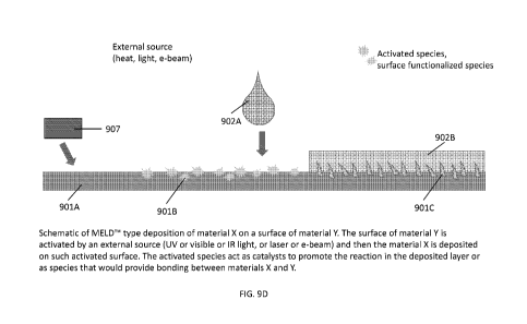
[00199] FIGS. 18A is a photograph of a solid-state additively-manufactured
aluminum
piece (partially surface finished) with embedded taggant.
[00200] FIG. 18B are photographs of the aluminum piece from FIG. 18A being
triggered
(irradiated) with a laser light pen (wavelength 405 nm, power < 5 mW) for few
seconds.
[00201] FIG. 18C are photographs (taken in dark) of the same aluminum
piece from
FIG. 18A after being irradiated with the laser pen light and showing
phosphorescent effects.
[00202] FIG. 19 is a schematic diagram showing potential tracking of
objects produced by
the solid-state additive manufactured process in a battlefield with e.g. IR-
sensing device. The
objects comprising IR-emitting or IR absorbing taggants are constituent parts
of e.g.
ammunition (bullets), riffles, helmets, vests, military vehicles, etc. and are
being detected by
triggering by IR light.
DETAILED DESCRIPTION OF VARIOUS EMBODIMENTS OF THE INVENTION
[00203] Reference will be made in detail to various exemplary embodiments
of the
invention. It is to be understood that the following text with exemplary
embodiments is not
intended as a limitation on the invention. Rather, the following text is
provided to give the
reader a more detailed understanding of certain aspects and features of the
invention. With
reference to the figures, the preferred embodiments of the present invention
will be herein
described for illustrative purposes, to illustrate the particular idea of the
invention, and by no
means as limitations. Any combination of different embodiments can be used, as
well. For
example, the word "primary" is intended only to suggest that other embodiments
may be
defined in terms of their relation to the embodiment initially described; it
is not meant to
indicate a preference for or the superiority of the presented version. As used
herein, the term
24
CA 03104289 2020-12-17
WO 2019/246251 PCT/US2019/037968
"coating material" is used interchangeably with "filler material" and
"feedstock material"; each
relate to an additive material which is fed through a throat of a rotating
stirring tool as
described in this disclosure. The additive material can also be referred to
interchangeably as a
"consumable" material.
[00204] In certain embodiments two dissimilar materials, e.g. polymer
(plastic) 102 to
metal 101 or metal 101 to polymer (plastics) 102 are joined together with the
solid-state
additive manufacturing process (FIGS. 1A and 1B). In other embodiments two
dissimilar
polymers (plastics) 102A and 102B are joined together (FIG. 1C). In yet
another embodiment,
two dissimilar metals (or metal alloys or MMCs or any combination of them)
101A and 101B, or
metals that cannot be welded together, are joined together (FIG. 1D).
[00205] In some embodiments, the joining process occurs between a
substrate 101 and
a layer 102 deposited by the solid-state additive manufacturing process, while
in other
embodiments, both, 101 and 102, are layers deposited by the solid-state
additive
manufacturing process.
[00206] In some embodiments, the plastic 102 is joined to the metal 101 by
way of an
inter-layer, where the inter-layer is a composite layer 103 (FIG. 1E). The
composite layer 103 is
composed of: (i) both materials, the polymer and the metal, in a form of e.g.
metal fibers or
metal particles dispersed in a polymer matrix, or (ii) carbon fibers or glass
fibers dispersed in
polymer matrix, or (iii) composition of other dissimilar materials.
[00207] In other embodiments, there are two or more interlayers involved
between the
metal 101 and the plastic 102A to be joined together (FIG. 1F). The interlayer
stack is composed
of but not limited to: plastic 102B/prepreg 104/plastic 102C, or plastic
102A/composite
103/plastic 102B, and where top plastic material 102A and the plastic
interlayers 102B and
102C are the same or different types of plastics.
[00208] In some embodiments, the interphase interlayer 105 is formed in
situ by the
solid-state additive manufacturing process and is different than the
previously described
interlayers (FIG. 1G). In another embodiment, the interface 105 is made by
surface
functionalization of the surface(s) that need to be joined by the solid-state
additive
manufacturing. As example only, such interface 105 is produced by in situ
chemical reaction of
CA 03104289 2020-12-17
WO 2019/246251 PCT/US2019/037968
the chemical species found on the surface of the material 101 need to be
bonded with the
material 102, when the species are in contact with the species of the material
102 or when they
are exposed to elevated temperatures and/or friction forces.
[00209] In some embodiments, sandwich structures, comprising but not
limited to metal
201A/plastic 202/metal 201B (FIG. 2A) or multiple stacks of metal 201A/plastic
202A/metal
201B/ plastic 202B/ metal 201C/plastic 202C/metal 201D/ (FIG. 2B), as ways
toward lightweight
structures, which are replacing bulk metal structures, are fabricated via
solid-state additive
manufacturing processes.
[00210] In specific embodiments, dissimilar parts are joined via solid-
state additive
manufacturing processes. As example only, already made metal part (e.g. plate,
sheet) 301A
and plastic part (plate, sheet) 302 are joined together side by side or
arranged in any other way
and overcoated with top metal layer 301B by a solid-state additive
manufacturing process
(FIG. 3A). In another embodiment, the metal part 301 and the plastic part 302A
are put close
together and joined by coating a plastic overlayer 302B with solid-state
additive manufacturing
system, as presented in FIG. 3B. In yet another embodiment, variety of parts,
metal parts 301A,
301B, 301C, plastic parts 302A, 302B, 302C and a composite part 303 are joined
together by
overcoating a metal layer 301D by a solid-state additive manufacturing (FIG.
3C). In yet other
embodiments, various shapes and sizes of multiple plastic, composite, prepreg
and/or metal
parts are joined together with overlayer deposited by the solid-state additive
manufacturing.
The deposited overlayer can be metal, plastic or composite layer.
[00211] In one embodiment, the solid-state additive manufacturing joining
is performed
in the presence of interlocks. The interlocks 406 can be in the metal part 401
(FIG. 4A)
subjected to the solid-state additive joining process, and the plastic layer
402 is being added, or
the interlocks 406 can be in the plastic part 402 that is being overcoated
with a metal layer 401
by the solid-state additive manufacturing process (FIG. 4B).
[00212] Furthermore, in some embodiments, the interlocks are additionally
functionalized to provide better bonding between the two materials needed to
be joined. For
this purpose, the interlocks 406 are subjected to a treatment (chemical or
physical treatment,
or combination of both) to functionalize the interlocks' surface, and thus,
form one
26
CA 03104289 2020-12-17
WO 2019/246251 PCT/US2019/037968
functionalized layer 405 or multiple-layer functionalized interfaces 405A,
405B, 405C, which
strengthen the bonding between the two materials or parts 401 and 402 to be
joined (FIG. 4C).
[00213] In some embodiments, the inter-locks can be of any shape, size and
periodicity;
some are presented in FIGS. 5A-5C. The interlocks 506A, 506B, 506C, 506D,
506E, 506F made in
e.g. metal substrate 501 could enable better bonding with the overlayer (metal
or plastic)
deposited by solid-state additive manufacturing (FIG. 5A). The interlocks like
506G, 506H, 5061,
506J, 506K, 506L and 506M, presented in FIG. 5B, are preferred embodiments in
this invention.
[00214] For example, dovetail-like interlocks 506G are the preferred
interlocks in this
invention, because they could provide better joining between two dissimilar
materials needed
to be joined. Furthermore, in some embodiments, the interlocks 506 could be
the same or
could vary in size, shape and depth along the surface of the layer 501 needed
to be joined with
a dissimilar overcoated material (FIG. 5C). In another embodiment, the
interlocks are periodic
and yet in another embodiment the interlocks appear non-periodically along the
surface of the
layer 501.
[00215] In one embodiment, the stack of multi-layers, all deposited via
the solid-state
additive manufacturing process, is fabricated. The individual layers in the
stack are joined
without interlocks. In another embodiment, the individual layers 601A, 602A,
601B, 602B, are
joined via interlocks 606A, 606B and 606C, which can be different from one
layer to another or
the same, as presented in FIG. 6.
[00216] In some embodiments, the consequent layer deposition by the solid-
state
additive manufacturing process can be done by changing the material
composition, and thus,
generating a functional gradient composition along the direction of increasing
the number of
layers (FIGS. 7A and 7B). For instance, the first layer is metal 701 that
needs to be joined to
plastic 702. With the aid of the solid-state additive manufacturing system,
interlayers with
701/702 mixture compositions are deposited. The compositions could be, but not
limited to
701/702 70/30 vol%, 50/50 vol% and 30/70 vol%. In certain embodiments, the
layers to be
joined 701 and 702, as well as 701/702 mixture interlayers, could be with the
same thickness
(FIG. 7A), or in other embodiments, they could be with different thicknesses
(FIG. 7B). In some
embodiments, the joining between the layers 701, 702 and 701/702 mixture
interlayers could
27
CA 03104289 2020-12-17
WO 2019/246251 PCT/US2019/037968
be with the aid of inter-locks 706A, 706B and 706C (FIG. 7C). Any number of
functionally-graded
interlayers is possible between the materials needed to be joined.
[00217] These interlayers can be any of the following compositions ranging
from
701/702 99.9/0.1 vol% to 701/702 0.1/99.9 vol%, preferably in the range
between 701/702
99/1 vol% and 701/702 1/99 vol%, and more preferred in the range between
701/702 95/5
vol% to 701/702 5/99 vol%, such as 10/90 vol% to 90/10 vol%, or 20/80 vol% to
80/20 vol%, or
such as 30/70 vol% to 70/30 vol%, or 40/60 vol% to 60/40 vol%, or 50/50 vol%,
or any range
within any one or more or combinations of these ranges and/or endpoints. The
functionally-
graded interlayers can be of the same or different thickness (FIG. 7A).
[00218] In certain embodiments, the functional grading occurs along the
thickness of the
deposited layers, but the composition changes smoothly and not as discrete
layers (FIG. 7D). In
some embodiments, the functional grading can be done in the transverse
direction of the solid-
state additive manufacturing deposition, as presented in FIG. 7E.
[00219] In some embodiments the solid-state additive manufacturing joining
between
two dissimilar materials, metal 801 and plastic 802, is done via interlayers,
different than those
described in the previous embodiments, as presented in FIG. 8. As an example
only, a polymer
layer 802 is joined to a steel substrate 801 via Zn-based coating 805A
deposited on the
substrate 801, then Cr-based coating 805B is deposited, which is then over-
coated with a hybrid
coating e.g. organo-silane primer 805C, and finally the polymer layer 802 is
deposited by the
solid-state additive manufacturing process. In certain embodiments, the
interlayers 805 are
added with the same solid-state additive manufacturing system as the main
layers 801 and 802
are deposited with. In other embodiments, the main layers 801 and 802 are
deposited by the
solid-state additive manufacturing, while the interlayers 805 are deposited by
other processes
known in the art, e.g. magnetron sputtering, thermal evaporation, e-beam
evaporation, spray
coating, spin-coating, knife coating, dip-coating, etc.
[00220] In some embodiments, the easily-flowing polymer composition (or
monomer,
oligomer, prepolymer composition) 902A, which during the solid-state additive
manufacturing
process is in the so-called visco-elastic state, can penetrate (diffuse) among
the metal grains
901A of the metal part (substrate) 901 that needs to be joined with the
polymer layer 902B
28
CA 03104289 2020-12-17
WO 2019/246251 PCT/US2019/037968
(FIG. 9A). Depending on the polymer (oligomer, monomer) and metal type
involved in the
solid-state additive manufacturing joining process, the polymer diffusion 901B
among the
intrinsic metal grains (lattices) or rearranged metal grains (lattices) during
the solid-state
process might occur. Since the metal is in the so-called malleable state, the
polymer (oligomer,
monomer) molecules can diffuse among the metal grains during the solid-state
additive
manufacturing process and act as an adhesive for the overlaying bulk polymer
layer 902B to the
metal layer 901 (FIG. 9A).
[00221] In another embodiment, a liquid crystalline polymer (LCP) or LC
oligomer 902A is
employed and deposited on a metal substrate (or part) 901 by the solid-state
additive
manufacturing process. The rod-like molecular structure of LCP might enables
preferential
orientation of the LCP molecules during the solid-state additive manufacturing
process yielding
a layer 902B with anisotropic properties, e.g. directional mechanical
properties (FIG. 9B).
[00222] In some embodiments, reactive compositions are used for deposition
by the
solid-state additive manufacturing process. As example only, such reactive
composition could
be composed of reactive polymers, prepolymers, oligomers and/or monomers and
initiators
902A (FIG. 9C). The reactive composition is added in the solid-state additive
manufacturing
system and during the deposition on a substrate, e.g. metal substrate 901 due
to the friction
and generated frictional heat, the composition further cross-links and forms a
highly cross-
linked coating (thermoset coating) 902B on top of the substrate 901.
[00223] In another embodiment, the deposited material 902A might be
irradiated with
an external source, e.g. UV light, visible light, IR light and/or electron
beam (e-beam) source
907, to further cross-link the deposited material 902A on the surface of a
substrate 901A into a
cross-linked layer 902B (FIG. 9D). In yet another embodiment, the deposited
reactive
composition 902A undergoes a reaction catalyzed by the species 901B found on
the surface of
substrate 901A on which the material 902A is deposited onto. For instance,
ions from the
surface 901B act as catalysts for the deposited reactive composition 902A and
form bonds 901C
between the two materials in situ. The final layer 902B is strongly bonded to
the substrate 901A
with the bonds 901C (FIG. 9D).
29
CA 03104289 2020-12-17
WO 2019/246251 PCT/US2019/037968
[00224] In yet another embodiment, the surface of the substrate 901A on
which a
second material 902A is being deposited on, is previously activated by heat,
light or e-beam
generated from the source 907, and the activated species on the surface 901B
act as catalysts
for the deposited layer 902B or as bonds between the two layers (FIG. 9D).
[00225] In some embodiments, dopants, reinforcing particles and or fibers
1008A, 1008B
and/or 1008C are used to strengthen the polymer 1002 that need to be joined to
a dissimilar
material (FIG. 10A). For example, the polymer material 1002 is doped with
reinforcing particles
1008A, such as metal/metal oxide particles, ceramic particles, carbon-based
particles, etc.
(FIG. 10A). Another example is when the polymer material is doped with fiber-
like reinforcers
1008B, such as glass fibers, carbon fibers, metal fibers or composite fibers
(e.g. Aramid, PAN,
etc.). The fibers can be continuous fibers or chopped fibers with nano-size or
micron-size
dimensions. In yet another example, the reinforcers are carbon nanotubes
(CNTs), which can be
single-wall, double-wall or multi-wall CNTs. In one embodiment, the
reinforcers are
polymer-wrapped CNTs. In yet another embodiment, functionalized fibers serve
as reinforcers.
[00226] In some embodiments, the dopants are microcapsules 1008C filled
with reactive
compounds or compounds having certain activity. As example only, the dopants
are
microcapsules 1008C filled with thermal initiator to cause additional cross-
linking during the
solid-state additive manufacturing deposition of the polymer material 1002. In
another
example, the dopants are microcapsules 1008C filled with an adhesion promoter
to provide
better adhesion between the polymer and metal material to be joined. In yet
another example,
the microcapsules 1008C are filled with liquid lubricant or compatibilizer in
order to provide
better mixing and compatibility between the polymer and metal materials.
[00227] In another embodiment, the dopants/reinforcers 1008 are added to
the metal
material 1001 (FIG. 10B). The dopants/reinforcers 1008 can be other metal
particles added to
the matrix metal 1001 (e.g. stainless steel). As an example, the particles
1008 are such particles
that are able to release Ag or Cu ions, and thus, yield anti-microbial
functionality of the metal
layer (stainless steel) 1001. In another embodiment, the particles 1008 are
ceramic particles,
e.g. SiC or BN, added to provide a reinforcing effect to the meta matrix 1001.
In yet another
example, the particles 1008 are carbon-based particles, e.g. carbon fibers,
CNTs, carbon black
CA 03104289 2020-12-17
WO 2019/246251 PCT/US2019/037968
to provide reinforcing effect and electrical conductivity. In another example,
the particles 1008
are fiber-like dopants.
[00228] In some embodiments, fiber-like reinforcers 1008 are used to
strengthen the
individual layers and/or the interface between the two consecutive dissimilar
layers. The
surface region of the material that it is deposited on and the added filler
material are in a
so-called malleable state during the solid-state additive deposition process
and both materials
are mixed together. The fiber reinforcers are mixed with both materials in the
interface region
and will further strengthen the interface. In another embodiment, the fiber-
like dopants 1008
are added during the solid-state deposition process only at the interface
between the two
dissimilar materials, e.g. metal 1001 and polymer 1002 (FIG. 10C) to provide
additional strength
at the interface. In another embodiment, the interface has inter-locks 1006
and the reinforcing
fibers 1008 are added in the inter-locks (FIG. 10D).
[00229] In some embodiments, in addition to the basic matrix material
compositional
changes in the direction of increasing number of deposited layers, e.g.
depositing the layers
metal 1101, metal/polymer blends 1101/1102 70/30 vol% and 1101/1102 30/70 vol%
and then
polymer layer 1102, the concentration of the added dopants (reinforcing
particles or fibers)
1108 is changing as well, as presented in FIG. 11A. The metal/polymer blends
can be in the
range of 5/95 vol% to 95/5 vol%, such as 10/90 vol% to 90/10 vol%, or 20/80
vol% to
80/20 vol%, or such as 30/70 vol% to 70/30 vol%, or 40/60 vol% to 60/40 vol%
or 50/50 vol%,
or any range within any one or more or combinations of these ranges and/or
endpoints.
[00230] In other embodiments, the dopants/reinforcers' type and
concentration can be
tailored throughout the deposited layers. As example only, two different
functional dopants or
reinforcers 1108A and 1108B are added in the materials, metal 1101 and polymer
1102, joined
via metal/polymer blends 1101/1102 70/30 vol% and 1101/1102 30/70 vol% as
presented in
FIG. 11B. The metal/polymer blends can be in the range of 5/95 vol% to 95/5
vol%, such as
10/90 vol% to 90/10 vol%, or 20/80 vol% to 80/20 vol%, or such as 30/70 vol%
to 70/30 vol%,
or 40/60 vol% to 60/40 vol%, or 50/50 vol%, or any range within any one or
more or
combinations of these ranges and/or endpoints.
31
CA 03104289 2020-12-17
WO 2019/246251 PCT/US2019/037968
[00231] In situ tailoring of the dopant/reinforcement particles 1108A and
1108B
concentrations is done during the solid-state additive manufacturing process
in order to
provide targeted properties in the top layers of the 3D structure built by the
solid-state additive
manufacturing process, e.g. to provide anti-corrosion, anti-wear, acoustic
protection or anti-
microbial activity. As an example, reinforcer 1108B provides the impact
strength of the
structure, while the dopant 1108A provides the desired anti-corrosion or anti-
wear or
anti-microbial functionality on the surface of the built structure.
[00232] In another embodiment, the gradient in the reinforcing fibers
(glass-, carbon,
metal-, polymer-, composite- fibers, CNTs, etc.) is achieved in addition to
the functionally-
graded layers comprising metal layer 1101, metal/polymer blend layers
1101/1102 70/30 vol%
and 1101/1102 30/70 vol% and top polymer layer 1002 (FIG. 11C). The
metal/polymer blends
can be in the range of 5/95 vol% to 95/5 vol%, such as 10/90 vol% to 90/10
vol%, or 20/80 vol%
to 80/20 vol%, or such as 30/70 vol% to 70/30 vol%, or 40/60 vol% to 60/40
vol%, such as
50/50 vol%, or any range within any one or more or combinations of these
ranges and/or
endpoints.
[00233] In yet another embodiment, the dopant/reinforcer 1108
concentration changes
occur within a single deposited layer 1101, where there are no changes in the
basic matrix
material (FIG. 11D).
[00234] In some embodiments, the dopant/reinforcing particles/fibers'
concentration is
changed along the direction of added layers yielding a positive concentration
gradient. In yet
another embodiment, the dopant/reinforcing particles/fibers' concentration is
changed along
the direction of added layers yielding a negative concentration gradient.
[00235] In some embodiments, the functionality of the deposited layers is
achieved via
the basic material prepared prior to the solid-state additive manufacturing
process or in situ
during the deposition process.
[00236] As example only, metal particles are added to a polymer powder or
granular
material during the solid-state additive manufacturing process. Depending on
the metal type
and concentration, the deposited polymer layer has certain functionalities,
which are different
than those of the basic polymer material. In one case, the layer made of a
polymer in situ mixed
32
CA 03104289 2020-12-17
WO 2019/246251 PCT/US2019/037968
with Cu particles, and consequently, deposited by way of the solid-state
additive manufacturing
process, exhibits anti-microbial activity in addition to increasing the
thermal and electrical
conductivity of the polymer layer. In another example, a polymer layer with
metal particles or
reinforcers could partially replace heavy metal structures and still have
properties similar to the
metal counterparts. In some embodiments, antimicrobial coatings are fabricated
by in situ
mixing of metal or polymer material with Ag or Cu nano-particles and deposited
on a substrate.
This approach is of particular interest in industries, like the ship-
manufacturing industry, where
the ship surface has to be resistant to biofilm formation.
[00237] In some embodiments, corrosion protection of metal surfaces is
achieved by
solid-state additive manufacturing deposition of a conductive polymer layer.
In yet another
embodiment, the anticorrosion functionality of the metal surface is achieved
by depositing a
non-conductive polymer.
[00238] In some embodiments, scratch-resistant top layer is achieved by
depositing a
self-healing polymer layer. As example only, a self-healing polymer usually
contains
microcapsules filled with photo-initiator and monomer. In a case of a scratch
or cut on the
surface of self-healing layer, the microcapsule(s) break and the initiator
reacts under UV and/or
visible light and cross-link the monomers, thus providing a polymer filling in
the layer's
scratch/cut.
[00239] In some embodiments, anti-wear layers or coatings are deposited by
the solid-
state additive manufacturing process. In another embodiments, shock-absorbent
layers are
deposited via solid-state additive manufacturing process between two metallic
or composite
layers. In one embodiment, the shock-absorbent layer is an elastomer.
[00240] In one embodiment, the solid-state additive manufacturing coating
deposited is
a Teflon-like coating. The fluoro-polymer coatings (known as "dry film
lubricants") are hard and
slick coatings with excellent corrosion- and chemical resistance and are non-
stick coatings that
significantly reduce friction and abrasion resistance.
[00241] In some embodiments, the parts' surfaces to be joined by the solid-
state
process(es) are not previously treated. In other embodiments, one or both
surfaces of the parts
needed to be joined are subjected to treatment (e.g. physical or chemical),
including but not
33
CA 03104289 2020-12-17
WO 2019/246251 PCT/US2019/037968
limited to: plasma etching, laser etching, reactive ion etching (RIE), corona
treatment, flame
treatment, ozone treatment, grafting, chemical etching (acid etching) or
functionalization, etc.,
provided by the source 1207, thus the untreated surface 1201A of the part to
be joined
transforms into treated surface or coating 1201B, as presented in FIG. 12A.
The surface
treatment usually provides increased surface roughness on a micron- and/or
nano-scale.
Depending on the type of the treatment, the initial surface 1201A surface
roughness can be
etched into the surface resulting in a surface 1201B or the surface treatment
can be "added" on
top of the surface, e.g. surface functionalization 1201C, as it is
schematically shown in FIG. 12B.
Consequently, the generated surface roughness 1201B or 1201C will provide
better bonding of
the dissimilar material 1202 deposited on top of the treated surface (FIG.
12C).
[00242] In particular embodiment, copper (Cu) layer is joined to an
aluminum (Al) layer
by solid-state additive manufacturing. The Al layer is deposited first, and
when the required
thickness is achieved, the deposition of the Cu layer occurs. Scanning
electron microscope
(SEM) images of Cu-Al interface of MELDTM type deposited layers are given in
FIG. 13A.
[00243] In another embodiment, steel and aluminum (Al) are joined via
interlocks.
SEM images of steel-Al interface around the square type interlock are
presented in FIG. 13B. In
other embodiments, steel and Al are joined via dovetail type interlock as
presented in FIG. 13C.
[00244] In some embodiments, the joint between two different materials is
"direct" as
presented in the SEM image in FIG. 13D for steel-Al. In other embodiments, by
adjusting the
MELDTM type processing conditions, the joint between two materials involves
formation of an
intermetallic layer, as presented with the SEM image for steel-Al in FIG. 13E.
In yet another
embodiment, the joint between two materials involves mechanical mixture of
both materials as
an interlayer, as presented with the SEM image for steel-Al given in FIG. 13F.
[00245] Furthermore, the following provides certain Aspects of the
taggants
incorporation in deposited layers, but should not be construed as limiting.
[00246] Aspect 1A. A MELDTM type 3D printed layer or object, or method of
manufacture
thereof, where the layer or object comprises at least one taggant that
uniquely responds to an
external triggering of a reading device, and thus, the layer originality can
be verified.
34
CA 03104289 2020-12-17
WO 2019/246251 PCT/US2019/037968
[00247] Aspect 2A. The layer, object, or method of Aspect 1, where the
layer originality is
verified with a light source generating light of certain wavelengths.
[00248] Aspect 3A. The layer, object, or method of any preceding Aspect,
where the layer
originality is verified with a heat-generating source.
[00249] Aspect 4A. The layer, object, or method of any preceding Aspect,
where the layer
originality is verified with an electric field generating device.
[00250] Aspect 5A. The layer, object, or method of any preceding Aspect,
where the layer
originality is verified by a magnetic field generating device.
[00251] Aspect 6A. The layer, object, or method of any preceding Aspect,
where the layer
originality is verified by a microscope.
[00252] Aspect 7A. The layer, object, or method of any preceding Aspect,
where the layer
is deposited in continuous solid-state additive manufacturing process by
continuous mixing the
taggant(s) with the feedstock material and their subsequent deposition.
[00253] Aspect 8A. The layer, object, or method of any preceding Aspect,
where the layer
is deposited in a continuous solid-state additive manufacturing process by
adding taggant(s) to
the feedstock material at certain time periods.
[00254] Aspect 9A. The layer, object, or method of any preceding Aspect,
where the layer
is deposited in a discontinuous (batch) solid-state additive manufacturing
method by adding
taggant(s) in particular batches to the feedstock material.
[00255] Aspect 10A. The layer, object, or method of any preceding Aspect,
where the
taggant is in situ generated during solid-state additive manufacturing
deposition.
[00256] Aspect 11A. The layer, object, or method of any preceding Aspect,
where the
taggant is generated by physical bonding or complexation of the components
added in the
solid-state additive manufacturing system.
[00257] Aspect 12A. The layer, object, or method of any preceding Aspect,
where the
taggant is generated by a chemical reaction among components added in the
solid-state
additive manufacturing system.
[00258] Aspect 13A. The layer, object, or method of any preceding Aspect,
where the layer
comprises an inert taggant that is activated by an external device.
CA 03104289 2020-12-17
WO 2019/246251 PCT/US2019/037968
[00259] Aspect 14A. The layer, object, or method of any preceding Aspect,
where the layer
comprises an inert taggant that is activated by applying external chemical(s).
[00260] Aspect 15A. The layer, object, or method of any preceding Aspect,
where the layer
comprises one, two or more taggants in a particular order along the deposited
layer.
[00261] Aspect 16A. The layer, object, or method of any preceding Aspect,
where the layer
comprises one, two or more taggants, which are activated only in
conjunction/concert with the
taggant(s) in the subsequent and/or underneath layers.
[00262] Aspect 17A. The layer, object, or method of any preceding Aspect,
where the layer
comprises one, two or more taggants with multiple levels of security.
[00263] Aspect 18A. The layer, object, or method of any preceding Aspect,
where a single
taggant responds to multiple readers (detectors) to reveal the hidden
information.
[00264] Aspect 19A. The layer, object, or method of any preceding Aspect,
where two or
more taggants are present, which upon triggering by a single reader reveal
multiple levels of
secured information.
[00265] Aspect 20A. The layer, object, or method of any preceding Aspect,
where two or
more taggants reveal multiple levels of secured information upon being
triggered by two or more
reading devices.
[00266] Aspect 21A. The layer, object, or method of any preceding Aspect,
where the layer
comprises a phosphor-type taggant(s).
[00267] Aspect 22A. The layer, object, or method of any preceding Aspect,
where the layer
comprises strontium aluminate doped with rare earth metal.
[00268] Aspect 23A. The layer, object, or method of any preceding Aspect,
where the layer
comprises up converting phosphor(s).
[00269] Aspect 24A. The layer, object, or method of any preceding Aspect,
where the layer
comprises taggants with blue light emission upon light excitation.
[00270] Aspect 25A. The layer, object, or method of any preceding Aspect,
where the layer
comprises taggant(s) with green light emission upon light excitation.
[00271] Aspect 26A. The layer, object, or method of any preceding Aspect,
where the layer
comprises taggant(s) with red light emission upon light excitation.
36
CA 03104289 2020-12-17
WO 2019/246251 PCT/US2019/037968
[00272] Aspect 27A. The layer, object, or method of any preceding Aspect,
where the layer
comprises taggant(s) with white light emission upon light excitation.
[00273] Aspect 28A. The layer, object, or method of any preceding Aspect,
where the layer
comprises taggant(s) with yellow light emission upon light excitation.
[00274] Aspect 29A. The layer, object, or method of any preceding Aspect,
where the layer
comprises taggant(s) with orange light emission upon light excitation.
[00275] Aspect 30A. The layer, object, or method of any preceding Aspect,
where the layer
comprises taggant(s) with indigo (purple) light emission upon light
excitation.
[00276] Aspect 31A. The layer, object, or method of any preceding Aspect,
where the layer
comprises taggant(s) with multiple-color light emission upon light excitation.
[00277] Aspect 32A. The layer, object, or method of any preceding Aspect,
where the layer
comprises distributed taggants in a controlled fashion, which upon light
excitation will emit colors
in a particular pattern.
[00278] Aspect 33A. The layer, object, or method of any preceding Aspect,
where the layer
comprises taggant(s) that will act in concert with the other layers revealing
specific color pattern.
[00279] Aspect 34A. The layer, object, or method any preceding Aspect,
where the layer
comprises photochromic taggant(s).
[00280] Aspect 35A. The layer, object, or method of any preceding Aspect,
where the layer
comprises thermochromic taggant(s).
[00281] Aspect 36A. The layer, object, or method of any preceding Aspect,
where the layer
comprises electrochromic taggant(s).
[00282] Aspect 37A. The layer, object, or method of any preceding Aspect,
where the layer
comprises two of more taggants that upon a certain triggering action react and
exhibit special
effects.
[00283] In particular embodiments, only one type of taggant is used in a
particular section
(layer) of the final part built by solid-state additive manufacturing or
throughout the whole object
(part) built by the solid-state additive manufacturing process.
37
CA 03104289 2020-12-17
WO 2019/246251 PCT/US2019/037968
[00284] In other embodiments, two or more taggants are used in the part
built by the
solid-state additive manufacturing process. The taggants can be mixed together
and distributed
throughout the particular deposited layer or can be distributed throughout the
whole part.
[00285] In some embodiments, to overcome the disadvantages of a single
taggant use or
single security application level, multi-level security solutions and/or
multiple taggants are used.
For instance, in one embodiment the taggant is "invisible" in the deposited
layer 1401, if an
external triggering/detecting action is not present (FIG. 14A). The taggant
responds in a certain
way 1401A, when exposed to a light of certain wavelength (FIG. 14B) triggered
by light source
1408A, it responds in a different way 1401B when exposed to a heat (elevated
temperature)
supplied by a heat source 1408B (FIG. 14C), and yet responds in a third way
1401C, when exposed
simultaneously to light of certain wavelength supplied by a light source 1408A
and heat supplied
by heat source 1408B (FIG.14D). Multiple types of taggants can also be used to
provide desired
responses to selected stimuli.
[00286] In another embodiment, two taggants are used, which are
"invisible" in the
deposited layer 1501, when there is no triggering action present (FIG. 15A).
When triggering
occurs, e.g. with exposure to certain light by a light source 1508A, only one
taggant shows its
effect 1501A (FIG. 15B). Under a different triggering action, e.g. at elevated
temperature supplied
by a heat source 1508B, the second taggant shows its effects 1501B (FIG. 15C),
and when both
triggering actions are present (light + heat) supplied by the sources 1508A
and 1508B, both
taggants exhibit their effects 1501A and 1501B (FIG. 15D). Under a very
different triggering action
1508C, the both taggants show effects 1501C very different effects than the
ones previously
exhibited or may react together and show the effect 1501C (FIG. 15E).
[00287] The light source used to trigger the taggant can be a lamp (such
as a UV, visible,
or infrared lamp), a light emitting diode, or a laser. The UV lamp can emit
light in UV-A, UV-B, or
UV-C bands. The laser can be chosen to emit one or more wavelengths anywhere
from ultraviolet
to infrared spectral range.
[00288] Non-limiting categories of laser sources include solid-state
lasers, gas lasers,
excimer lasers, dye lasers, and semiconductor lasers. An excimer laser is a
non-limiting example
of a laser emitting at ultraviolet frequencies, while a CO2 laser is a non-
limiting example of a laser
38
CA 03104289 2020-12-17
WO 2019/246251 PCT/US2019/037968
emitting at infrared frequencies. The choice of the laser will depend on the
particular wavelength
of light emitted and its relative absorption by the taggant(s). In one
embodiment, the laser is a
tunable laser which allows adjustment of the output wavelength. Descriptions
of various laser
sources are available in the art including Thyagarajan, K., Ghatak, Ajoy,
Lasers: Fundamentals and
Applications, Springer US, 2011, ISBN-13:9781441964410, incorporated by
reference herein, as
well as The Encyclopedia of Laser Physics and Technology (available online at
https://www.rpphotonics.com/encyclopedia.html).
[00289] The heat source used to trigger the taggant(s) can be any object
that produces or
radiates heat, such as an infrared lamp, electrical heating element, flame,
combusting materials,
waste heat sources, and the like.
[00290] In particular embodiments, a phosphor material or a combination of
two or more
phosphors are used as taggants. Phosphor, in general, is a material that
exhibits luminescence,
which term covers both, phosphorescence and fluorescence (FIG. 16A). Phosphors
are often
consisting of transition metal compounds or rare-earth compounds used as
dopants in a matrix
(host) material.
[00291] In other embodiments, up-converting phosphors are used as
taggants.
Up-converting phosphors are microscopic ceramic powders that convert invisible
infrared light
wavelengths to visible colored light (FIG. 16B). For instance, up-converting
phosphors can emit
visible green, red, orange or blue colors, when triggered with an infrared
light (e.g. IR laser pen).
There is an anti-stokes shift that separates emission peaks from the infrared
excitation peak.
Essentially, these taggants light up when hit with an infrared light. In
combination with other
taggant technologies, they can be utilized as a step in a multi-level security
solution. The
mechanism behind the up-converting phosphors is the so-called up-conversion,
where the
sequential absorption of two or more photons results in the light emission at
shorter wavelength
than the excitation wavelength. It is also known as anti-Stokes emission and
therefore the
materials are known as anti-Stokes phosphors. Example is excitation with IR
light and emission in
the visible spectral range. Lanthanide-doped materials, such as fluorides
NaYF4, NaGdF4, LiYF4,
YF3, CaF2 or oxides such as Gd203 are doped with certain amounts of lanthanide
ions. The most
common lanthanide ions used in photon up-conversion are the pairs erbium-
ytterbium
39
CA 03104289 2020-12-17
WO 2019/246251 PCT/US2019/037968
(Er3+,Yb3+) or thulium-ytterbium (Tm3+, Yb3+). Usually ytterbium ions are
added to absorb light
at around 980 nm and transfer it to the upconverter ion. If the upconverter
ion is erbium, then a
characteristic green and red emission is observed, while when the upconverter
ion is thulium,
the emission includes near ultraviolet, blue and red light.
[00292] An example of a phosphor material is strontium aluminate
(SrA1204), which can
be "activated" with a suitable dopant, e.g. europium (SrA1204:Eu), and then it
can act as a
phosphor with long persistence of phosphorescence. Besides strontium
aluminate, other
aluminates can be used as the host matrix for the rare-earth or transition-
metal dopants. The
matrix (as well as the dopant) affects the emission wavelength of the dopant
ion. In general,
strontium aluminate phosphors produce green and blue emissions with excitation
wavelengths
ranging from 200 to 450 nm. The wavelength for its green emission is 520 nm,
its aqua or blue-
green emission is at 505 nm, and the blue version emits at 490 nm. For
europium-dysprosium
doped aluminates, the peak emission wavelengths are 520 nm for SrA1204, 480 nm
for SrA1407,
and 400 nm for SrA112019. Cerium- and manganese- doped strontium aluminate
(SrA112019:Ce,Mn) shows intense narrowband phosphorescence at 515 nm, when
excited by
ultraviolet light.
[00293] In some embodiments, a variety of strontium aluminates are used
and more
specifically the Eu doped Sr-aluminates. Several emission spectra of Eu-doped
strontium
aluminates are given in FIG. 16C, where the emitted visible color ranges from
purple, blue, green,
orange to red.
[00294] In other embodiments, other types of phosphors are used as
taggants in the solid-
state additive deposits, such as but not limited to:
[00295] YAI03:Ce (YAP), blue emission (370 nm)
[00296] Y2Si05:Ce (P47), blue emission (400 nm)
[00297] CdW04, blue emission (475 nm)
[00298] ZnO:Zn (P15), blue emission (495 nm)
[00299] CdS:In, green emission (525 nm)
[00300] Y3A15012:Ce (YAG), green emission (550 nm)
[00301] Zn(0.5)Cd(0.4)S:Ag (HS), green emission (560 nm)
CA 03104289 2020-12-17
WO 2019/246251 PCT/US2019/037968
[00302] LiF/ZnS:Cu,AI,Au (NDg), green emission (565 nm)
[00303] Gd202S:Eu, red emission (627 nm)
[00304] Zn(0.4)Cd(0.6)S:Ag (HSr), red emission (630 nm)
[00305] MgW04, white emission (500 nm)
[00306] Y202S:Pr, white emission (513 nm), etc.
[00307] In some embodiments, and especially for military applications,
among different
taggant materials and devices, those emitting in the Infrared (IR) region or
identified with IR-light
are especially important classes of covert taggants. Infrared (IR) light is
part of the
electromagnetic radiation with wavelengths ranging from 0.75 p.m to 1000 p.m.
For military
applications, the IR wavelength is usually limited to 15 p.m.
[00308] Certain materials can emit IR light through chemiluminescence,
photoluminescence or electro-luminescence. There are three general groups of
IR emitting
materials: organic IR emitting dyes, lanthanide IR emitters, and semiconductor
IR emitters. Many
organic dyes have been developed especially for NIR bimolecular imaging and
common organic
NIR fluorophores include cyanine, oxazine and rhodamine dyes. The
emission/fluorescence peaks
of these dyes are between 700-850 nm. Organic dyes with fluorescence maxima
extending to far
near IR and into short wave IR can be achieved by the formation of metal ion
complexes. The
most notable group of metals whose ions are capable of narrow band infrared
emission is the
lanthanide series with atomic numbers 57 to 71 (lanthanum to lutetium).
Lanthanide infrared
phosphors can also be hosted in inorganic matrices. These inorganic host
materials include
fluoride and oxyfluoride optical glasses, such as NaYF, SiO2¨A1203¨NaF¨YF3,
and oxide glass/
ceramics including SiO2, ZrO2, Y203, and Y3A15012 (yttrium aluminum garnet;
YAG). These
inorganic host materials are generally optically transparent, especially in
the IR spectral region.
Infrared emissions of lanthanide are often achieved through photoluminescence.
Well known IR
emission wavelengths from lanthanide ions are generally in the 1-3 p.m
regions, but also there
are known several trivalent lanthanide ions that have possible emission
transitions in the 3-5 p.m
spectral region.
41
CA 03104289 2020-12-17
WO 2019/246251 PCT/US2019/037968
[00309] In a certain embodiment, the MELDTM type solid-state additive
deposits are
containing up-converting phosphors that are especially useful in night
searching for materials or
objects with IR light.
[00310] In some embodiments, microfibers, e.g. carbon fibers, or chopped
microfibers, are
embedded in objects produced by a solid-state additive manufacturing process
and used as
taggants, where the particular fiber morphology can be distinguished with a
more sophisticated
detector, e.g. with a microscope.
[00311] In a certain embodiment, photochromic taggant(s) are incorporated
in
MELDTM type deposited layers or parts. The taggant responds by changing a
color or appearance
of color upon exposure to light of certain wavelengths.
[00312] In another embodiment, thermochromic taggant(s) are incorporated
in
MELDTM type deposited layers or parts. The taggant responds by appearance of
color or changing
a color upon exposure to heat.
[00313] In yet another embodiment, electrochromic taggant(s) are
incorporated in
MELDTM type deposited layers or parts. The taggant responds by appearance of
color or changing
a color upon electric field is applied to the layer/part, which is very useful
for conductive parts.
[00314] In some embodiments, the taggant is added only in specific
layer(s) during the
solid-state additive manufacturing deposition (FIG. 17A). In other
embodiments, the taggant is
added in all the layers, which compose the object produced by the solid-state
additive
manufacturing process.
[00315] In yet another embodiment, each taggant is applied in a different
layer of the
structure in a particular sequence. In the authentication (checking) step, the
particular sequence
of taggants' distribution is verified by use of an authentication (read-out or
reader) device, which
can be a laser light excitation device in the case of used photochromic
taggants, or a heat-
generating device in the case of thermo-chromic taggants, or their combination
which needs
more sophisticated detecting device. In FIG. 17B multiple layers are deposited
by a solid-state
additive manufacturing process, where each layer contains different phosphors,
which upon
excitation with IR laser pen emit specific visible colors in a certain
sequence of the deposited
layers.
42
CA 03104289 2020-12-17
WO 2019/246251 PCT/US2019/037968
[00316] In another embodiment, different taggants are added within one
layer deposited
by a solid-state additive manufacturing process in a specific fashion known to
limiting number of
people (FIG. 17C). The taggants are detected by scanning the layer with a
reader. For instance,
different phosphors or up-converting phosphors are distributed in the layer in
a sequence that is
being revealed upon the layer (part) is excited with the excitation
wavelengths that these
phosphors/ up-converting phosphors respond.
[00317] In particular embodiment, a photoluminescent taggant (PL pigment
MHB-5BA,
Zhejiang Minhui L&T Co.) is added in a solid-state deposited aluminum layer
(FIG. 18A). After
exposure of the layer or particular zones of the layer with blue light
supplied by a laser pen
(405 nm wavelength, <5 mW power) for few seconds (FIG. 18B) and after
discontinuing the light
exposure, the layer i.e. the irradiated zone of the layer, emits green light
due to the
photoluminescent effect (FIG. 18C).
[00318] In some embodiments, the embedded taggants in military parts made
by the solid-
state additive manufacturing process can be sensed with IR-sensing device. As
example only, the
solid-state-deposited objects that are constituent parts of e.g. ammunition,
bullets, helmets,
military vehicles, and so on, can be tracked and detected from the air and not
left behind for the
enemy (FIG. 19).
[00319] According to embodiments, the solid-state additive manufacturing
machine,
tooling and processes may be or include any machine, tool or process described
in or depicted in
any one or more or combinations of U.S. Application Publication Nos.
2008/0041921,
2010/0285207, 2012/0009339, 2012/0279441, 2012/0279442, 2014/0130736,
2014/0134325,
2014/0174344, 2015/0165546, 2016/0074958, 2016/0107262, 2016/0175981,
2016/0175982,
2017/0043429, 2017/0057204, 2017/0216962, 2018/0085849, 2018/0361501, and
International
Publication Nos. WO 2013/002869 and WO 2019/089764, which are each hereby
incorporated
by reference herein in their entirety. According to one embodiment, the solid-
state additive
manufacturing machine comprises a friction-based fabrication tool comprising:
a non-
consumable body formed from material capable of resisting deformation when
subject to
frictional heating and compressive loading and a throat defining a passageway
lengthwise
43
CA 03104289 2020-12-17
WO 2019/246251 PCT/US2019/037968
through the body and shaped for exerting normal forces on a material in the
throat during
rotation of the body.
[00320] According to another embodiment, the solid-state additive
manufacturing
machine comprises a non-consumable member having a body and a throat; wherein
the throat
is shaped to exert a normal force on a consumable material disposed therein
for imparting
rotation to the coating material from the body when rotated at a speed
sufficient for imposing
frictional heating of the coating material against a substrate; wherein the
body is operably
connected with a downward force actuator for dispensing and compressive
loading of the
consumable material from the throat onto the substrate and with one or more
actuators or
motors for rotating and translating the body relative to the substrate;
wherein the body
comprises a surface for trapping the consumable material loaded on the
substrate in a volume
between the body and the substrate and for forming and shearing a surface of a
coating on the
substrate.
[00321] Other specific embodiments include friction-based fabrication
tools comprising:
(a) a spindle member comprising a hollow interior for housing a consumable
coating or filler
material disposed therein prior to deposition on a substrate; wherein the
interior of the spindle
is shaped to exert a normal force on the consumable material disposed therein
for rotating the
consumable material during rotation of the spindle; (b) a downward force
actuator, in operable
communication with the spindle, for dispensing and compressive loading of the
consumable
material from the spindle onto the substrate and with one or more motors or
actuators for
rotating and translating the spindle relative to the substrate; and wherein
the spindle comprises
a shoulder surface with a flat surface geometry or a surface geometry with
structure for
enhancing mechanical stirring of the loaded consumable material, which
shoulder surface is
operably configured for trapping the loaded consumable material in a volume
between the
shoulder and the substrate and for forming and shearing a surface of a coating
on the substrate.
[00322] In some embodiments, the throat has a non-circular cross-sectional
shape.
Additionally, any filler material can be used as the consumable material,
including consumable
solid, powder, or powder-filled tube type coating materials. In the case of
powder-type coating
material, the powder can be loosely or tightly packed within the interior
throat of the tool, with
44
CA 03104289 2020-12-17
WO 2019/246251 PCT/US2019/037968
normal forces being more efficiently exerted on tightly packed powder filler
material. Packing of
the powder filler material can be achieved before or during the coating
process. Further provided
are tooling configurations comprising any configuration described in this
application, or any
configuration needed to implement a method according to the invention
described herein,
combined with a consumable filler material member. Thus, tooling embodiments
of the invention
include a non-consumable portion (resists deformation under heat and pressure)
alone or
together with a consumable coating material or consumable filler material
(e.g., such
consumable materials include those that would deform, melt, or plasticize
under the amount of
heat and pressure the non-consumable portion is exposed to).
[00323] Another aspect of the present invention is to provide a method of
forming a
surface layer on a substrate, such as repairing a marred surface, building up
a surface to obtain a
substrate with a different thickness, joining two or more substrates together,
or filling holes in
the surface of a substrate. Such methods can comprise depositing a coating or
filler material on
the substrate with tooling described in this application, and optionally
friction stirring the
deposited coating material, e.g., including mechanical means for combining the
deposited
coating material with material of the substrate to form a more homogenous
coating-substrate
interface. Depositing and stirring can be performed simultaneously, or in
sequence with or
without a period of time in between. Depositing and stirring can also be
performed with a single
tool or separate tools, which are the same or different. Particular methods
include depositing a
coating on a substrate using frictional heating and compressive loading of a
coating material
against the substrate, whereby a tool supports the coating material during
frictional heating and
compressive loading and is operably configured for forming and shearing a
surface of the coating.
[00324] In embodiments, the tool and consumable material preferably rotate
relative to
the substrate. The tool can be attached to the consumable material and
optionally in a manner
to allow for repositioning of the tool on the coating material. Such
embodiments can be
configured to have no difference in rotational velocity between the coating
material and tool
during use. The consumable material and tool can alternatively not be attached
to allow for
continuous or semi-continuous feeding or deposition of the consumable material
through the
throat of the tool. In such designs, it is possible that during use there is a
difference in rotational
CA 03104289 2020-12-17
WO 2019/246251 PCT/US2019/037968
velocity between the consumable material and tool during the depositing.
Similarly,
embodiments provide for the consumable material to be rotated independently or
dependently
of the tool.
[00325] Preferably, the consumable material is delivered through a throat
of the tool and
optionally by pulling or pushing the consumable material through the throat.
In embodiments,
the consumable material has an outer surface and the tool has an inner
surface, wherein the
outer and inner surfaces are complementary to allow for a key and lock type
fit. Optionally, the
throat of the tool and the consumable material are capable of lengthwise
slideable engagement.
[00326] Even further, the throat of the tool can have an inner diameter
and the
consumable material can be a cylindrical rod concentric to the inner diameter.
Further yet, the
tool can have a throat with an inner surface and the consumable material can
have an outer
surface wherein the surfaces are capable of engaging or interlocking to
provide rotational
velocity to the consumable material from the tool. In preferred embodiments,
the consumable
filler or coating material is continuously or semi-continuously fed and/or
delivered into and/or
through the throat of the tool. Shearing of any deposited consumable material
to form a new
surface of the substrate preferably is performed in a manner to disperse any
oxide barrier coating
on the substrate.
[00327] Yet another aspect of the present invention is to provide a method
of forming a
surface layer on a substrate, which comprises filling a hole in a substrate.
The method comprises
placing powder of a fill material in the hole(s) and applying frictional
heating and compressive
loading to the fill material powder in the hole to consolidate the fill
material. In yet another
embodiment, the MELDTM type machine, in addition to including a tool described
in this
specification or the Appendices, includes a substrate. Materials that can
serve as the consumable
filler material or as the substrate(s) can include metals and metallic
materials, polymers and
polymeric materials, ceramic and other reinforced materials, as well as
combinations of these
materials. In embodiments, the filler material can be of a similar or
dissimilar material as that of
the substrate material(s). The filler material and the substrate(s) can
include polymeric material
or metallic material, and without limitation include metal-metal combinations,
metal matrix
46
CA 03104289 2020-12-17
WO 2019/246251 PCT/US2019/037968
composites, polymers, polymer matrix composites, polymer-polymer combinations,
metal-
polymer combinations, metal-ceramic combinations, and polymer-ceramic
combinations.
[00328] In one particular embodiment, the substrate(s) and/or the filler
material are metal
or metallic. The filer material, or the substrate(s) can be independently
selected from any metal,
including for example Al, Ni, Cr, Cu, Co, Au, Ag, Mg, Cd, Pb, Pt, Ti, Zn, or
Fe, Nb, Ta, Mo, W, or an
alloy comprising one or more of these metals. In embodiments, the substrate(s)
and/or the filler
material are polymeric material. Non-limiting examples of polymeric materials
useful as a filler
material include polyolefins, polyesters, nylons, vinyls, polyvinyls,
acrylics, polyacrylics,
polycarbonates, polystyrenes, polyurethanes, and the like. In still yet
another embodiment, the
filler material is a composite material comprising at least one metallic
material and at least one
polymeric material. In other embodiments, multiple material combinations can
be used for
producing a composite at the interface.
[00329] The filler materials can be in several forms, including but not
limited to: 1) metal
powder or rod of a single composition; 2) matrix metal and reinforcement
powders can be mixed
and used as feed material; or 3) a solid rod of matrix can be bored (e.g., to
create a tube or other
hollow cylinder type structure) and filled with reinforcement powder, or
mixtures of metal matric
composite and reinforcement material. In the latter, mixing of the matrix and
reinforcement can
occur further during the fabrication process. In embodiments, the filler
material may be a solid
metal rod. In one embodiment, the filler material is aluminum.
[00330] According to embodiments, the filler material and/or the
substrate(s) are
independently chosen from plastics, homo polymers, co-polymers, or polymeric
materials
comprising polyesters, nylons, polyvinyls such as polyvinyl chloride (PVC),
polyvinylidene chloride
(PVDC), polyvinylidene fluoride (PVDF), polyacrylics, polyethylene
terephthalate (PET or PETE),
Polybutylene terephthalate (PBT), polyamides (PA), Nylons (Ny6, Ny66),
polylactide,
polycarbonates, polystyrenes, polyurethanes, engineering polymers such as
polyetherketone
(PEK), polyetheretherketone (PEEK), polyaryletherketone (PAEK),
polyetherketoneketone
(PEKK), Acrylonitrile butadiene styrene (ABS), Polyphenylene sulfide (PPS),
Polysulphone (PSU),
polyphenylsulfone (PPSU), Polyphenylene oxide (PPO), Polyphenylene sulfide
(PPS),
Polyoxymethylene plastic (POM), polyphthalamide (PPA), polyarylamide (PARA),
and/or
47
CA 03104289 2020-12-17
WO 2019/246251 PCT/US2019/037968
polyolefins such as high density polyethylene (HDPE), low density polyethylene
(LDPE), cyclic
olefin copolymers (COC), polypropylene, composites, mixtures, reinforcement
materials, or a
metal matrix composite comprising a metal matrix and a ceramic phase, wherein
the metal
matrix comprises one or more of a metal, a metal alloy, or an intermetallic,
and the ceramic phase
comprises a ceramic, and independently chosen from metallic materials, metal
matrix
composites (MMCs), ceramics, ceramic materials such as SiC, TiB2 and/or A1203,
metals
comprising steel, Al, Ni, Cr, Cu, Co, Au, Ag, Mg, Cd, Pb, Pt, Ti, Zn, Fe, Nb,
Ta, Mo, W, or an alloy
comprising one or more of these metals, as well as combinations of any of
these materials.
[00331] According to one embodiment, any of the taggant(s) described
herein are added
to or mixed with any of the above filler (also known herein as feedstock)
material which is fed
through the tool. According to another embodiment, the taggant(s) are layered
on top of the
substrate prior to deposition of the filler material on top of the substrate.
In both cases, the
rotating tool of the solid-state additive manufacturing machine mixes the
taggant(s) during
deposition and plastic deformation of the layer deposited by the solid-state
additive
manufacturing process.
[00332] According to one embodiment, the layer is deposited in continuous
solid-state
additive manufacturing process by continuous mixing the taggant(s) with the
feedstock material
and their subsequent deposition.
[00333] According to another embodiment, the layer is deposited in a
continuous solid-
state additive manufacturing process by adding taggant(s) to the feedstock
material at certain
time periods.
[00334] According to another embodiment, the layer is deposited in a
discontinuous
(batch) solid-state additive manufacturing process by adding taggant(s) in
particular batches to
the feedstock material.
[00335] According to another embodiment, the taggant is in situ generated
during solid-
state additive manufacturing deposition.
[00336] According to another embodiment, the taggant generated by physical
bonding or
complexation of the components added in the solid-state additive manufacturing
system.
48
CA 03104289 2020-12-17
WO 2019/246251 PCT/US2019/037968
[00337] According to another embodiment, the taggant is generated by a
chemical
reaction among components added in the solid-state additive manufacturing
system.
[00338] The present invention has been described with reference to
particular
embodiments having various features. In light of the disclosure provided
above, it will be
apparent to those skilled in the art that various modifications and variations
can be made in the
practice of the present invention without departing from the scope or spirit
of the invention. One
skilled in the art will recognize that the disclosed features may be used
singularly, in any
combination, or omitted based on the requirements and specifications of a
given application or
design. When an embodiment refers to "comprising" certain features, it is to
be understood that
the embodiments can alternatively "consist of" or "consist essentially of" any
one or more of the
features. Any of the methods disclosed herein can be used with any of the
compositions disclosed
herein or with any other compositions. Likewise, any of the disclosed
compositions can be used
with any of the methods disclosed herein or with any other methods. Other
embodiments of the
invention will be apparent to those skilled in the art from consideration of
the specification and
practice of the invention.
[00339] It is noted in particular that where a range of values is provided
in this
specification, each value between the upper and lower limits of that range, to
the tenth of the
unit disclosed, is also specifically disclosed. Any smaller range within the
ranges disclosed or that
can be derived from other endpoints disclosed are also specifically disclosed
themselves. The
upper and lower limits of disclosed ranges may independently be included or
excluded in the
range as well. The singular forms "a," "an," and "the" include plural
referents unless the context
clearly dictates otherwise. It is intended that the specification and examples
be considered as
exemplary in nature and that variations that do not depart from the essence of
the invention fall
within the scope of the invention. Further, all of the references cited in
this disclosure are each
individually incorporated by reference herein in their entireties and as such
are intended to
provide an efficient way of supplementing the enabling disclosure of this
invention as well as
provide background detailing the level of ordinary skill in the art.
49