Note: Descriptions are shown in the official language in which they were submitted.
CA 03105605 2021-01-04
WO 2020/010057 PCT/US2019/040256
OPEN-CIRCUIT ELECTROLUMINESCENCE
CROSS-REFERENCE TO RELATED APPLICATIONS
[0001] This application claims priority to U.S. Utility Application No.
16/027,471
filed on July 5, 2018 and U.S. Utility Application No. 16/376,643 filed on
April 5, 2019.
The entire disclosure of each of the above applications is incorporated herein
by
reference.
FIELD
[0002] The present disclosure relates to methods and devices for
generating
light from electroluminescent devices under open-circuit conditions. The
present
disclosure further relates to uses of the present disclosure in the service of
test
methods and methods of detection.
BACKGROUND AND SUMMARY
[0003] This section provides background information related to the
present
disclosure which is not necessarily prior art. This section provides a general
summary
of the disclosure, and is not a comprehensive disclosure of its full scope or
all of its
features.
[0004] Previous alternating-current electroluminescent devices require a
first
lead, wire or conductor to provide current through a first electrode to the
device and a
second lead, wire or conductor at a distinct location to transmit current
across the
electroluminescent material back to the source of electrical current.
Applicant has
discovered that electrodes and leads that close a circuit from and back to a
power
supply or source of electrical energy are not required. It is only necessary
to supply a
time-varying electrical signal with a single lead, wire or conductor at a
predetermined
level to the electroluminescent device to create an electric field at the
electroluminescent device and to provide a means whereby the electric field is
increased sufficiently across the electroluminescent device to excite the
electroluminescent device. This can be achieved by providing in close
proximity to the
electroluminescent device an object or substance that increases the electric
field
across the EL device.
[0005] Further areas of applicability will become apparent from the
description
provided herein. The description and specific examples in this summary are
intended
1
CA 03105605 2021-01-04
WO 2020/010057 PCT/US2019/040256
for purposes of illustration only and are not intended to limit the scope of
the present
disclosure.
DRAWINGS
[0006] The drawings described herein are for illustrative purposes only
of
selected embodiments and not all possible implementations, and are not
intended to
limit the scope of the present disclosure.
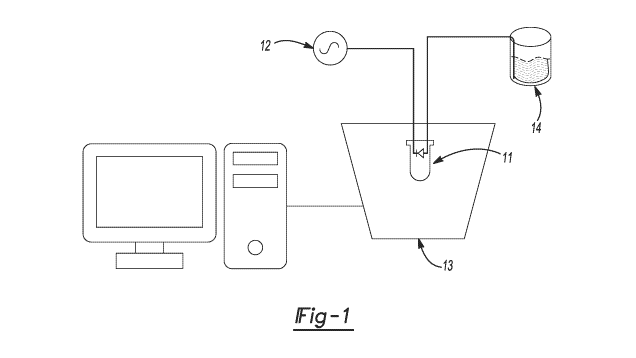
[0007] Figure 1 is a diagram depicting an example embodiment of a system
using an LED lamp for producing electroluminescence in proportion to the
amount of
water in a container.
[0008] Figure 2 is a graph depicting the relationship between light
intensity and
water volume using an embodiment of the present disclosure.
[0009] Figure 3 is a diagram depicting an example embodiment of a system
using a phosphor layer for producing electroluminescence in proportion to
water
quantity.
[0010] Figure 4 is a graph depicting the relationship between light
intensity and
water volume using an embodiment of the present disclosure.
[0011] Figure 5 is a diagram depicting an example embodiment of a system
for
producing electroluminescence in response to the amount of water in a
container
where electrical energy is interrupted by a dielectric layer.
[0012] Figure 6 is a graph depicting the relationship between light
intensity and
water volume using the experimental setup shown in Figure 5.
[0013] Figure 7 is a diagram depicting an example embodiment of a system
for
producing electroluminescence in proportion to the amount of water in a
container
where electrical energy is supplied to two LEDs in series.
[0014] Figure 8 is a diagram of an example embodiment of a system for
producing electroluminescence in proportion to an analyte in a sample using
transmission of electrical energy through the sample.
[0015] Figure 9 is a diagram of an example embodiment of a system for
producing electroluminescence in proportion to an analyte in a sample.
[0016] Figure 10 is s a diagram of an example embodiment having a planar
electroluminescent device for obtaining images of objects placed in contact.
[0017] Figure 11 is an image of a fingerprint obtained with the device of
Figure
10.
2
CA 03105605 2021-01-04
WO 2020/010057 PCT/US2019/040256
[0018] Figure 12 is s a diagram of an example embodiment having a planar
electroluminescent device with a dielectric layer for obtaining images of
objects placed
in contact.
[0019] Figure 13 is an image of a fingerprint obtained with the device of
Figure
12.
[0020] Figure 14 is s a diagram of an example embodiment having a planar
electroluminescent device with two dielectric layers for obtaining images of
objects
placed in contact.
[0021] Figure 15 is an image of a fingerprint obtained with the device of
Figure
14.
[0022] Figure 16 is a graph showing the influence of various liquids on
light
emission.
[0023] Figure 17 is a diagram of a device for producing
electroluminescence
using a commercial LED immersed in a conductive medium.
[0024] Figure 18 is a diagram of a device for producing
electroluminescence
using a phosphor-coated electrode immersed in a conductive medium.
[0025] Figure 19 is a diagram of a device for producing
electroluminescence
using a phosphor-coated electrode with the power supply and/or electric field-
increasing body also immersed in a conductive medium.
[0026] Figure 20 is a diagram of a portion of an EL device of the
invention used
to image an object and having a phosphor layer on a transparent electrode.
[0027] Figure 21 is a diagram of a portion of an EL device of the
invention used
to image an object and having a phosphor layer on a portion of a dielectric
layer-
coated transparent electrode.
[0028] Figure 22 is a diagram of a portion of an EL device of the
invention used
to image an object and having a phosphor layer sandwiched between dielectric
layers
on a transparent electrode.
[0029] Figure 23 is a diagram of a portion of an EL device of the
invention used
to image an object and having multiple phosphor layers sandwiched between
dielectric layers on a transparent electrode.
[0030] Figure 24 is a diagram of a portion of an EL device of the
invention used
to image an object and having a metal nanoparticle layer and phosphor layer
sandwiched between dielectric layers on a transparent electrode.
3
CA 03105605 2021-01-04
WO 2020/010057 PCT/US2019/040256
[0031] Figure 25 is a diagram of a portion of an EL device of the
invention used
to image objects and having a phosphor layer 4 in several segments sandwiched
between dielectric layers on a transparent electrode.
[0032] Figure 26 is a diagram depicting an example embodiment of a system
for producing electroluminescence in which a chosen object or body produces
differing intensity light by varying the input electrical signal.
[0033] Figure 27 is a diagram depicting an example embodiment of a system
for producing electroluminescence in which a water-filled hose is used to
transmit
time-varying electrical energy.
[0034] Figure 28 is a graph showing the variation of light intensity with
water-
filled hose length using the system of Figure 27.
[0035] Figure 29A is a diagram depicting an apparatus used in embodiments
of
the present disclosure.
[0036] Figure 29B is a graph showing the luminance response of an LED to
time-varying input voltage according to an embodiment of the present
disclosure.
[0037] Figure 29C is a graph showing change in light intensity
(luminance) as a
function of modulating DC input voltage into a power source producing an AC
signal
that is transmitted to an LED according to an embodiment of the present
disclosure.
[0038] Figure 30A is a schematic diagram describing an example embodiment
of a system for electroluminescence measurement of a contained fluid where an
electrical terminal is in direct contact with the fluid.
[0039] Figure 30B is a schematic diagram describing an example embodiment
of a system for electroluminescence measurement of a contained fluid where an
electrical terminal remotely senses the fluid.
[0040] Figure 31A is a schematic diagram describing an example embodiment
of a system for electroluminescence measurement of an object where a circuit
component is in direct contact with the object.
[0041] Figure 31B is a schematic diagram describing an example embodiment
of a system for electroluminescence measurement of an object where a circuit
component remotely senses the object.
[0042] Figure 32 is a schematic diagram describing an example embodiment
of
a system for electroluminescence measurement of an object using a transformer.
[0043] Figure 33 is a diagram describing an example embodiment of a
system
for electroluminescence measurement of both the type and quantity of an
unknown
4
CA 03105605 2021-01-04
WO 2020/010057 PCT/US2019/040256
liquid. Corresponding reference numerals indicate corresponding parts
throughout the
several views of the drawings.
DETAILED DESCRIPTION
[0044] Example embodiments will now be described more fully with
reference
to the accompanying drawings.
[0045] The present disclosure concerns methods, materials and devices for
producing quantifiable electroluminescence. The present invention further
concerns
methods, materials and devices for producing electroluminescence at open
circuit,
termed open-circuit electroluminescence (OCEL). In particular, the present
disclosure
concerns methods of detecting and measuring a property of a material, object
or
substance based on the ability of the property to cause the generation of
electroluminescence in such a method.
[0046] In the present disclosure, a physical property of an object is
determined
by a method involving measuring a change in electromagnetic radiation emitted
by an
electroluminescent device in proximity to the object. The terms change or
alter, as
used throughout the present disclosure, includes both increases and decreases
in the
intensity of electromagnetic radiation as well as changes in frequency or
frequency
range of the electromagnetic radiation emitted by the electroluminescent
device.
[0047] In some embodiments, time-varying electrical signal from a power
source is transmitted to one terminal of an electroluminescent device. An
object is set
in close proximity to a second terminal of the electroluminescent device, the
object
configured to cause a change in electromagnetic radiation of the
electroluminescent
device. The change in electromagnetic radiation of the electroluminescent
device is
measured by an electromagnetic radiation detector and related to a physical
property
of the object.
[0048] The present disclosure concerns methods, materials, and devices
for
producing electroluminescence at open circuit, termed open-circuit
electroluminescence (OCEL). In particular, the present disclosure concerns
methods
of measuring a property of an object based on the ability of the property to
interrupt
the propagation of electrical signal in an open-circuit configuration and,
therefore,
cause a change in electromagnetic radiation of an electroluminescent device.
In the
present disclosure, open-circuit describes an electronic circuit where a time-
varying
electrical signal is transmitted from a power source to an electroluminescent
device
CA 03105605 2021-01-04
WO 2020/010057 PCT/US2019/040256
and other optional circuit components while the electronic circuit remains
incomplete.
Applicant has discovered that the use of the second additional electrodes and
leads
that close a circuit from a power source to the electroluminescent device and
back to
the power supply are not required. The electrical signal in an open-circuit
configuration
is particularly responsive to changes to physical properties of the media
through which
it propagates. The present methods take advantage of this responsiveness to
the
changes to physical properties of the media through which the electrical
signal
propagates. Here, the changes to electrical signal across an
electroluminescent
device are detected and related to changes to physical properties of the media
through which the electrical signal propagates. In this application, the
medium through
which the electrical signal propagates is, as described herein generally
referred to as
an 'object and can also include, but is not limited to, a material or a
circuit component.
[0049] In one embodiment there is provided a method for measuring a
physical
property of an object comprising:
a. transmitting a time-varying electrical signal from a power source to an
electroluminescent device, wherein the electroluminescent device
remains at open circuit;
b. positioning an object in close proximity to a terminal of the
electroluminescent device while the time-varying electrical signal is
transmitted to the electroluminescent device, such that a change in the
physical property of the object alters the time-varying electrical signal
across the electroluminescent device and thereby changes intensity of
electromagnetic radiation from the electroluminescent device;
c. measuring the change in intensity of electromagnetic radiation emitted
by the electroluminescent device; and
d. relating the measured change in intensity of electromagnetic radiation to
a physical property of the object.
[0050] In another embodiment there is provided a method for measuring a
property of an object comprising:
transmitting a time-varying electrical signal from a power source through
a single electrical terminal to an electroluminescent device, wherein the
electroluminescent device remains at open circuit at all times;
positioning an object in close proximity to an electroluminescent device
while the time-varying electrical signal is transmitted to the
electroluminescent
6
CA 03105605 2021-01-04
WO 2020/010057 PCT/US2019/040256
device, such that the object increases the amplitude of the time-varying
electrical signal across the electroluminescent device and thereby generates
light from the electroluminescent device;
measuring intensity of the light emitted by the electroluminescent device;
and
relating the measured light intensity to the property of the object.
[0051] In
another embodiment the method further comprises measuring the
intensity of light and relating the light intensity to presence, position or
quantity of the
object or substance.
[0052] In
another embodiment there is provided a method for measuring
a property of a material, object or substance comprising:
transmitting a time-varying electrical signal from a power source through
a single electrical terminal to an electroluminescent device, wherein said
electroluminescent device comprises an electrode and a phosphor material
layer deposited on a surface of the electrode, and wherein the
electroluminescent device remains at open circuit at all times;
positioning an object in close proximity to an electroluminescent device
while the time-varying electrical signal is transmitted to the
electroluminescent
device, such that the object increases the amplitude of the time-varying
electrical signal across the electroluminescent device and thereby generates
light from the electroluminescent device;
measuring intensity of the light emitted by the electroluminescent device;
and
relating the measured light intensity to the property of the object.
[0053] In
a further embodiment the method above further comprises measuring
the intensity of light and relating the light intensity to presence, position
or quantity of
the object or substance.
[0054] In
another embodiment, there is provided a method for measuring a
property of a fluid comprising:
transmitting a time-varying electrical signal from a power source through
a single electrical terminal to an electroluminescent device through the
fluid,
wherein the electroluminescent device remains at open-circuit at all times;
positioning an object in close proximity to an electroluminescent device
while the time-varying electrical signal is transmitted to the
electroluminescent
7
CA 03105605 2021-01-04
WO 2020/010057 PCT/US2019/040256
device, such that the object increases the amplitude of the time-varying
electrical signal across the electroluminescent device and thereby generates
light from the electroluminescent device;
measuring intensity of the light emitted by the electroluminescent device;
and
relating the measured light intensity to the property of the fluid.
[0055] Definitions
[0056] Circuit Component: An electronic circuit is composed of individual
circuit
components, such as resistors, capacitors, inductors, solenoids, transformers,
thermocouple, thermopile, electrochemical cells, power supplies, filters,
diodes, and
transistors. Circuit components are operably coupled to the electronic
circuit. In some
embodiments, conductive wires are used to operably couple a circuit component
to an
electronic circuit. Once operably coupled to an electronic circuit, a circuit
component
can impact an electrical signal transmitting through the electronic circuit.
[0057] Close Proximity: indicates any close spatial relationship
effective for
increasing the altering the electric field at the electroluminescent device
and includes
actual physical contact, or a zero separation distance. Distances greater than
zero,
i.e. non-contact, can also be used as long as the separation permits electric
field
alteration. Typical distances in practice will generally be on the order of 1
cm or less,
and frequently 1 mm or less. A layer of dielectric material will provide a
physical
barrier between an electroluminescent device and the test object and thus
determine
a distance of physical separation. The dielectric so used can have a thickness
in the
range of 0.001 to 1 mm.
[0058] Capacitor Electrode: A capacitor electrode is defined as an
electrode
with differential electrical potential across its ends. Analogous to a
capacitor whose
'plates store charges of opposite polarity, i.e., positive and negative, a
capacitor
electrode holds unequal electrical potentials across its length resulting in a
non-zero,
residual electric field. The presence of this residual electric field will
impact the
electrical signal propagating along the capacitor electrode. A capacitor
electrode can
be one dimensional, e.g., wire, two-dimensional, such as a plate, or three-
dimensional, i.e., hemispherical shell.
[0059] Contained Liquid: A contained liquid refers to a liquid whose
physical
properties including, but not limited to, volume, height, and dielectric
constant are of
interest. The liquid is stored in a container and its physical properties are
measured.
8
CA 03105605 2021-01-04
WO 2020/010057 PCT/US2019/040256
The liquid may be flammable, such as gasoline. The liquid may resist, block,
or
conduct the propagation of electrical signal.
[0060] Contained Solid: A contained solid refers to a solid whose
physical
properties including, but not limited to, volume, height, and dielectric
constant are of
interest. The solid is stored in a container and its physical properties are
measured.
The solid may be one piece or unit such as a slab or block, or it may be a
collection of
solid pieces, of similar or varying sizes, e.g. powders or granular materials.
The solid
may resist, block, or conduct the propagation of electrical signal. The
present methods
may also be used, for example, to assess moisture content, chemical
composition, or
electrical conductivity of metals.
[0061] Contained Gas: A contained gas is an object in gaseous phase whose
physical properties including, but not limited to volume, pressure,
temperature,
dielectric constant, or moisture content are of interest. The object in a
gaseous phase
can also refer to a mixture of different gasses whose ratio(s) are to be
determined.
The gas can also include a vapor of a liquid.
[0062] It is to be understood that the term object as used throughout the
application is considered to mean individual objects or things as well as
quantities of a
material or substance such as a liquid that may be contained in a container,
or a
length of wire or quantity of sheet, film or foil, etc. The term object may be
used
interchangeably with material, substance, or object.
[0063] The property of the object or substance can be any of a variety of
physical or chemical properties. In various embodiments illustrated below, the
property can be one of a group selected from volume, mass, area, length,
distance,
concentration in a solution, pH, ionic strength, ratio of two substances in
admixture,
polarity, conductivity, capacitance, and temperature. Various example formats
and the
means of using the present methods based thereon as a way of detecting,
measuring
or quantifying a property of the object or substance are described in more
detail below
in several non-limiting example embodiments.
[0064] Light-Emitting Diodes (LED): In some embodiments, of the present
methods, the electroluminescent device is a light emitting diode or LED.
Conventional
LEDs feature a semiconductor chip surrounded by an epoxy shell with anode and
cathode wires protruding. The semiconductor chip is doped to have p and n
regions
and create a p-n junction. A hallmark of LEDs is that current flow is
unidirectional. In
the present disclosure it has been found that the choice of which electrode is
9
CA 03105605 2021-01-04
WO 2020/010057 PCT/US2019/040256
connected to the power supply is immaterial. Representative semiconductor
materials
found in LEDs useable in the present methods include GaAs, AlGaAs, GaAsP,
AlGaInP, GaP, GaAsP, AlGaP, InGaN, GaN, and ZnSe. Such LEDs are commercially
available and individual lights are available to produce any color in the
visible
spectrum. The methods of the present disclosure can involve the use of more
than
one LED bulb to produce electroluminescence. Arrays of a two- or three-
dimensional
shape are within the scope of the present methods as are assemblies of LEDs of
different emission colors.
[0065] In another aspect of the present methods the electroluminescent
device
comprises an electrode and at least one phosphor material deposited as a layer
on a
surface of the electrode. In some embodiments, the phosphor material layer
covers a
discrete region of a surface of the electrode. In some embodiments, a phosphor
material layer may cover a plurality of discrete regions of a surface of the
electrode.
The regions may be of any shape or dimensions and when a plurality of regions
occur
may be the same or different in size and shape. In certain embodiments wherein
a
plurality of different phosphor materials is used and wherein each region is
covered
with a single phosphor material, each of the different phosphor materials may
be
chosen to emit light of a different color. In this manner, various patterns
may be
produced, or different colors of light may result when the regions are small.
A well-
known example is the generation of white light by the mixing of red, green,
and blue.
[0066] In another embodiment, the phosphor material layer comprises an
admixture of different phosphor materials. This may be performed as another
method
of producing new or mixed colors as described above. In yet another embodiment
a
phosphor material may be combined into or embedded in a dielectric material.
[0067] Electrodes: The electrode used in the present methods may be of
any
practical or convenient shape or geometry as long as it is capable of bearing
a layer of
phosphor material on a surface. In some embodiments, the electrode may be
planar.
In some embodiments, the electrode may be curved. The electrode may
advantageously be optically transparent such as glass coated with Indium-tin-
oxide
(ITO), fluorine-doped tin oxide (FTO), 5n02, Al-doped ZnO, Ga-doped ZnO, or
other
ternary or quaternary transition metal oxides as are known in the art. Glass
coated
with graphene, carbon nanotubes, and metal nanoparticles and/or nanowires are
also
considered within the scope of usable electrode materials.
CA 03105605 2021-01-04
WO 2020/010057 PCT/US2019/040256
[0068] It is anticipated that ancillary materials, such as conductors,
metallic
elements - clips, screws, nuts/bolts, pins etc. may be used in the
construction and
assembly of devices for performing the methods of the present disclosure.
Selection
of such materials is within the ability of the skilled person and does not
depart from the
inventive concept disclosed herein.
[0069] Phosphors: Phosphor materials usable in the present disclosure can
be
any known substance or material known to generate electromagnetic radiation by
application of an alternating or direct electrical signal . Exemplary
materials can be
selected from the group consisting of semiconductor particles, doped
semiconductor
particles, elemental Si particles, elemental Ge particles, quantum dots,
fluorescent
monomers, fluorescent oligomers, fluorescent polymers, phosphorescent
monomers,
phosphorescent oligomers, phosphorescent polymers and mixtures thereof.
Phosphor
materials may also have at least one of the properties of exhibiting
fluorescence,
delayed fluorescence or phosphorescence. In some embodiments, the phosphor is
selected from a list of conductive wire and incandescent elements, such as
tungsten
wire and gold nanoparticles, wherein the phosphor emits electromagnetic
radiation,
such as infrared radiation, in response to application of an electrical
signal.
[0070] Particulate Phosphor Materials: In some embodiments, phosphor
materials are advantageously provided in the form of small particles,
typically of a size
less than about 0.1 mm (100 micrometers). In some embodiments, the particles
will be
less than about 1 micrometer. In other embodiments the particles will be
nanoparticles
in a size range of about 1-100 nm. In one embodiment nanoparticles are
composed of
a quantum dot semiconducting core material and a shell of a distinct
semiconducting
material. The core and the shell are typically composed of type II¨VI, IV¨VI,
and III¨V
semiconductors, for example CdS/ZnS, CdSe/ZnS, CdSe/CdS, and InAs/CdSe. In
some embodiments, the electroluminescent device comprises a quantity of
nanoparticles of a material type known in the art to be capable of generating
electroluminescence. Commonly these particles are made of inorganic
semiconductor
materials. One class of such electroluminescent materials comprises ZnS doped
with
a second metal. Incorporating small amounts of dopant elements in the
nanocrystals
enables adjusting of the color or wavelength of the electroluminescence
emission from
the nanoparticles. Included among these are ZnS doped with transition metals
or rare
earth metals. Representative examples include Mn (yellow-orange emission), Cu
(green emission), Al, Sm, Tm, Er, Nd, or Eu. Other usable materials include
11
CA 03105605 2021-01-04
WO 2020/010057 PCT/US2019/040256
semiconductors containing group III and group V elements, such as indium
phosphide
(InP), gallium arsenide (GaAs), and gallium nitride (GaN). Undoped and doped
semiconductor particles may optionally be oxide-coated.
[0071] In
another embodiment nanoparticles include a family of particles
synthesized with the aid of a porous support material as disclosed in commonly
owned co-pending US Patent Application Serial Nos. 15/240,271 and US
15/240,407.
Such materials may be used with or without the support material being present.
[0072]
Particles as used in the present application are not limited to any
particular shape and may have different shapes, including spheres, cubes,
rods,
wires, or plates, or a mixture of shapes within any given sample portion.
[0073] In
some embodiments, the phosphor material will comprise a continuous
layer of an organic luminescent material. A plethora of such compounds are
known in
the literature and used at present, e.g. in producing thin film devices.
Listings of such
materials are found in many standard treatises on the subject. Commonly used
OLED
materials include polymeric materials such as polyphenylene (PPP),
polyphenylene
vinylene (PPV), polyfluorene, polyaniline, polythiophene
(PT), and
polyethylenedioxythiophene (PDOT), and small molecules, such as Alq3, metal
phthalocyanines, and iridium or ruthenium organometallic complexes. The use of
any
such material is considered within the scope of the present methods. Devices
containing two or more layers with different organic luminescent material in
each layer
are specifically considered to be usable in the methods of the present
disclosure,
particularly when more than one color of light is to be produced or when
producing a
composite color by combining different color emitters as is commonly done to
produce
white light by combination of red, green and blue light emission.
[0074] In
some embodiments, the electroluminescent device further comprises
the use of dielectric materials as layers or coatings. For example, a
dielectric coating
over a surface of the phosphor layer opposite the transparent electrode. In
some
embodiments, the electroluminescent device further comprises a dielectric
coating
between the transparent electrode and the phosphor layer. Dielectric coatings
may,
alternatively be used both over a surface of the phosphor layer opposite the
transparent electrode and between the transparent electrode and the phosphor
layer.
Layers as used herein includes liquid materials applied and, if necessary,
dried in
place. Layers may be applied as a pre-manufactured thin film or as a tape. The
thickness of the layer of dielectric material may be determined and adjusted
as
12
CA 03105605 2021-01-04
WO 2020/010057 PCT/US2019/040256
needed and by reference to the numerous examples reported in the patent and
technical literature. Typical layers may range from 1 micron to 1 mm, for
example and
may optionally be of uniform thickness. The method of application of
dielectric layer is
not limited to any particular technique and may include dipping, applying a
liquid layer
and spreading, spin coating and other ways generally known in the art.
[0075] Dielectric Materials: Materials useful as dielectric materials in
the
present methods include, without limitation, BaTiO3, SrTiO3, barium strontium
titanate, calcium copper titanate, nitrile rubber, vinyl glove material,
paraffin, polymers
including polyethylene, polyimide, poly(dimethylsiloxane), polystyrene,
poly(methyl
methacrylate), polypropylene, polyethylene terephthalate, polyurethanes, nylon
polymers, acrylonitrile-butadiene rubber, vinyl rubber, glass, and graphene.
Mixed
dielectric materials are contemplated for use as well as using more than one
discrete
dielectric material in combination.
[0076] Object: as used in the present description refers to substances,
materials and articles which may be conductive also are generally considered
to be
included. An exemplary listing includes, without limitation, metals, metal
alloys, other
solid substances of any shape or size, including granular or particulate
materials and
their mixtures, liquids chosen from among polar liquids, as well as mixtures
of two or
more liquids in any proportion, solutions containing dissolved solutes, other
conductive materials such as solid or liquid conductive polymers are
considered within
the scope of the materials useful in the methods of the present disclosure.
Living
bodies, including plants and animals, parts of living bodies, a portion of a
body tissue
or a tissue section can all serve in this capacity in the present methods. As
mentioned
above, in some methods and applications an added circuit component can also
serve
as the object as described below. A more expansive description of exemplary
materials is set forth in U.S. patent application Serial No. 16/027,421.
[0077] Where the object is a liquid or gaseous substance, it is to be
understood
that the liquid or gas may be enclosed within a vessel or container. Said
vessel or
container may contact the electroluminescent device. Common vessels and
containers include, cups, test strips, test tubes, microwells, microwell
strips or plates,
and other conventional containers in common laboratory use. In such
embodiments,
the vessel or container comprises one or more walls having a thickness and the
thickness establishes a separation distance between the electroluminescent
device
and the substance that alters the electric field when used in the present
methods.
13
CA 03105605 2021-01-04
WO 2020/010057 PCT/US2019/040256
[0078] Physical property: includes any measurable property of an object
or a
substance including, without limitation, volume, mass, area, length, distance,
position,
orientation, speed, acceleration, displacement, density, concentration in a
solution,
pH, ionic strength, chemical composition, ratio of two substances in
admixture,
polarity, electrical potential, electrical charge content, conductivity,
resistivity,
capacitance, temperature, magnetic permeability, electric permittivity,
refractive index,
current density, vibration, oscillation, displacement, strain, stress,
pressure,
reflectivity, transparency, color, relative brightness, texture, rigidity,
geometry,
moisture content, absorptivity, energy, intensity, amplitude, frequency, mass-
to-charge
ratio, impurity, connectivity, mobility, viscosity, and pattern.
[0079] Power Source: The power source in some embodiments can be a cold
cathode fluorescent lamp (CCFL) inverter. CCFL inverter operates at high
voltage
(few volts to tens of kilovolts) and high frequency (10-50kHz). CCFL are often
used for
backlighting liquid crystal display (LCD) panels. The CCFL models include for
example: JKL components (BXA-24529, BXA-601), TDK (CXA-M10M-06Y15R, CXA-
P1612-VJL, CXA-L0505-NJL), etc. CCFL circuits normally operate at an input
voltage
of 0-24 VDC. The voltage output of CCFL can be adjusted with modifying the
inverter
circuit elements and/or changing the input voltage. The latter was
accomplished with
the use of batteries, AC/DC transformer (adapters), and/or a lab-grade
variable direct
current (DC) power source. In particular, VOLTEQ HY3006D is a regulated linear
DC
power source and is continuously adjustable at 0-30 VDC and 0-6A. Plug & play
systems are also within the scope of the present disclosure. In this case, the
power
supply is the typical North American/European power outlet with single-phase
unit
which has a 0-110/220VAC output voltage and frequency of 50/60 Hz. Other
commercial wave generators can also be used. For instance, the SIGLENT SDG805
5MHz 125MSa/s Arbitrary Waveform Generator was used to generate time-varying
electrical signal of various waveforms, including sine, square, ramp, pulse,
and
arbitrary/custom waveforms. The wave generator was further used to generate
voltage and frequency sweeps ranging IVppl <20 volts and f < 5 MHz, where Vpp
and
f represent the peak-to-peak voltage and wave frequency, respectively.
[0080] Time-varying electrical signal: as used in the present disclosure,
includes modulating electrical signals such as an alternating current having a
sinusoidal waveform of a wide range of frequencies. Frequencies useful in the
practice of the present methods can range from 1 Hz to 200 kHz, or in some
14
CA 03105605 2021-01-04
WO 2020/010057 PCT/US2019/040256
embodiments from 20 kHz to 50 kHz. Other forms of modulated amplitude signal
that
provide a change with respect to time are considered to be within the scope of
the
invention such as square waves, sawtooth waves and one or more pulsed
electrical
signals. The characteristics of an electrical signal include amplitude,
frequency,
waveform, phase angle, etc. Therefore, altering an electrical signal may refer
to
changing at least one of these characteristics. In some embodiments, the time-
varying
electrical signal switches between one or more states, such as a square wave,
to
improve system performance and/or to reduce power consumption.
[0081] Transmitting Media: The time-varying electrical energy is
transmitted
from the power source to the electroluminescent device by a transmitting
conductor.
Any material capable of transmitting an electrical signal, viewed as an
oscillating
electric field, can be used as a transmitting medium in the present methods.
Conventional metal wires, leads, and connectors, including gold, silver,
copper and
aluminum may be used. Due to the lack of any required conductive path back to
the
power supply however, the choice of material for transmitting time-varying
electrical
power to the electroluminescent device is broader. In some embodiments, the
transmitting conductor can be a fluid, more particularly, a liquid.
Advantageously, the
liquid may be an electrically conductive liquid. Water and aqueous solutions
containing salts, for example can be used in this capacity. In embodiments of
the
present disclosure wherein the time-varying electrical power is transmitted to
the
electroluminescent device by a fluid, it has been discovered that the light
intensity
generated by the electroluminescent device is proportional to the quantity of
the fluid.
Such methods performed in accordance with this embodiment can therefore serve
as
a way of determining the quantity of the fluid, e.g. its mass or volume. More
particularly, the method can serve as a way to determine the length of a
column of
fluid contained in a tube that contains the fluid. In other embodiments, the
light
intensity generated by the electroluminescent device is proportional to
another
property of the fluid. These other properties include for example,
conductivity,
dielectric constant, polarity, volume, concentration of a solute, or pH. Yet
other
embodiments can use a combination of two or more different materials, e.g. a
conductive wire and a liquid-filled tube. In embodiments where the
transmitting
conductor or medium comprises a fluid, the material or object in close
proximity to the
electroluminescent device may be a simple metallic wire, such as one terminal
of a
commercially available LED lamp.
CA 03105605 2021-01-04
WO 2020/010057 PCT/US2019/040256
[0082] In some embodiments, the transmitting medium will be positioned
between the electroluminescent device and the power source. In still other
embodiments, the transmitting medium may fully or partially surround the
electroluminescent device, in two dimensions or even completely envelop in
three
dimensions. In such formats, the electroluminescent device may be partially or
fully
covered with a dielectric material, but the methods of the present disclosure
are not
limited to these cases and no dielectric layer or barrier is required.
[0083] Conventional devices and apparatuses for producing
electroluminescence feature a source of electric current transmitted through a
wire to
a lead or electrode coupled or connected to an electroluminescent device and
further
having a second lead or electrode that conducts current through a wire back to
the
source of electric current to close the electrical circuit, a so-called
"closed-circuit"
configuration. Applicant has discovered that the use of the second additional
electrodes and leads that close a circuit from a power supply or source of
electrical
energy to the electroluminescent device and back to the power supply are not
required. In other words, the electroluminescent device is at "open circuit"
and yet
produces light. It is only necessary to supply a time-varying electrical
signal to the
electroluminescent device and provide a means whereby the electric field is
increased
sufficiently in the region of space around the electroluminescent device. This
can be
achieved by providing in close proximity to the electroluminescent device an
object or
substance that increases the electric field across the EL device. Without
wishing to be
bound by any particular theory of operation, substances, materials and objects
which
can serve this purpose in the methods of the present disclosure include those
which
can store electric charge, i.e. demonstrate capacitance.
[0084] Further, it has been found that the time-varying electrical energy
can be
transmitted to the electroluminescent device through other types of
transmission
media. Representative transmission media can include liquids such as water,
gases
such as air, and solids.
[0085] In operation, the methods of the present disclosure for producing
open-
circuit electroluminescence (OCEL) provide numerous advantages compared to the
conventional closed-circuit systems. Prior art closed-circuit technology
operates in a
manner governed by the capacitive characteristics of the electrodes and
dielectric and
emissive layers. The present methods are sensitive to any environmental
variations in
the properties of the electrode(s), EL device(s), dielectric layer(s),
transmission media,
16
CA 03105605 2021-01-04
WO 2020/010057 PCT/US2019/040256
and the material or the substance that causes the enhancement of electric
signal
across the EL device. The responsiveness to environmental conditions brings
about
advantageous operational and design flexibility characteristics which (without
limitation) include:
[0086] 1. Several substances can be examined simultaneously. The
present methods and systems can examine various materials and their capacitive
and/or (electromagnetic) conductive properties without the need to change any
of the
required elements of the system, i.e., time-varying power source, the
energized
electrode, as well as the emissive EL device. Dielectric layers are optional
and can be
a combination of various material/substances. This feature is uniquely of
interest for
the following applications: sensors, detectors, analytical instruments, etc.
[0087] 2. Pattern recognition. Using a combination of EL material
and/or
dielectric layers, the OCEL system can detect patterns. This feature is
particular
interest for pattern recognition technologies, such as fingerprint
characterization,
tissue structural examination, etc. The pattern recognition capability has a
resolution
of 2nm.
[0088] 3. The emissive EL layer can be changed for optimal results.
As
suggested in the below experiments, various phosphors respond best within a
certain
range of frequencies and electric field strengths. The ability to change the
EL layer
within the same system broadens the experimental conditions under which OCEL
can
operate.
[0089] 4. Operates wirelessly. In the presence of a strong
electromagnetic
field, an OCEL system can operate without the need for a physical contact
between
the time-varying power source and the electrodes.
[0090] 5. Operates within various media. As demonstrated below, OCEL
can operate while submerged in polar (conductive) media. In this case, a water
bath
can serve as either the hot electrode and/or the substance which enables
strengthening of the electric field across the EL device.
[0091] 6. Operates in conjunction with other optical and electrical
devices.
Luminometers, spectrometers, CCD cameras, fiber optics, passive and adaptive
optics can be coupled with the OCEL device to transmit the light output into a
communicable signal.
[0092] 7. Requires small input power to operate. The OCEL operates at
or
below a few watts.
17
CA 03105605 2021-01-04
WO 2020/010057 PCT/US2019/040256
[0093] 8. Efficient. OCEL converts the majority of the input power
into
emission. The capacitive characteristic of OCEL eliminates the power waste
(heat,
current leak, etc.) associated with competing technologies.
[0094] 9. Safe. OCEL operates within the RMS electrical current range
of
1-200 pA which is well below the Occupational Safety and Health Administration
guidelines (< 3 mA).
[0095] 10. Free form. The OCEL system is not limited to a specific
geometry
of the subcomponents. Existing EL devices are only offered in planar
(sandwich) or
co-planar formats. Various 1D, 2D,& 3D format OCEL devices have been
successfully
tested.
[0096] 11. EL material can be cast into shapes and in some cases held
in
place with dielectric material and/or the electrode. Unlike LEDs, the emissive
layer can
be formed into the desired shape. The shape will emit light when energized.
This
characteristic is of particular interest for consumer goods, entertainment,
and lighting
applications.
[0097] 12. Multiple devices can be coupled. More than one OCEL device
can be operated from the same time-varying power source.
[0098] 13. Tunable emission color. Multiple EL materials can be used
for
optimal frequency and/or electrical current range. In addition, this feature
allows for
the production of emissions with various colors.
[0099] 14. Tunable resolution. Various EL materials can be used to
modify
the resolution of the EL device.
[0100] 15. Tunable EL layer lifetime. Existing EL devices use
electrodes
with finite light absorption, such as the ITO glass. This means that higher
voltages
must be applied in order to operate the EL device at the desired light output.
Higher
voltages lower the lifetime of the EL material. OCEL works with substances
that help
enhance the local electric field (such as water) where no absorption is
expected. The
lower required voltage increases the lifetime of the EL device.
[0101] 16. Emissive layer can be coated with insulating material for
improving durability and enhancing device lifetime.
[0102] 17. EL layer can be applied onto the hot electrode or on the
surface
of the material or substance that helps to enhance the electric field across
the EL
device or be an independent layer. This feature will allow for a variety of
applications,
in particular, wireless applications.
18
CA 03105605 2021-01-04
WO 2020/010057 PCT/US2019/040256
[0103] 18. Works without the need for a support material. All existing
EL
technologies depend on electrodes, as the support member, for holding the EL
device
and dielectric layer in place. Free-form OCEL works also in environments where
the
EL material is floatin (unattached) in a container.
[0104] 19. Works independent of the direction of the applied time-
varying
electric energy. Unlike other unidirectional, diode-like EL devices, OCEL
works
regardless of the direction (positive-to-negative or negative-to-positive) of
input
voltage. This means that the EL device can be energized in any orientation.
The
signal can be with a positive or negative offset. The time average of the
signal can be
below or above zero.
[0105] 20. Improved contrast ratio: The use of a combination of EL
material
and/or different dielectric layers allows the production of a system whose
light output
for electrical energy El and E2=(E1)/2 are easily distinguishable. This
feature makes
OCEL uniquely sensitive to small variations of the electrical energy applied
across the
EL layer.
[0106] 21. Tunable dielectric layer: the change in the thickness
(distance
between the EL device and the conductive body), or the surface area of the
electrode
and/or the conductive body can change the light emission intensity. In
addition, the
light intensity can change depending on the type of dielectric used (ex.
solutions of
different dielectric constant).
[0107] Substances and Materials that Increase the Electric Field -
Substances,
materials and objects which exhibit electrical conductivity also are generally
thought to
be included in this category. Metals and metal alloys are representative
exemplary
materials. Metals useful in the practice of the present disclosure include,
without
limitation, gold, silver, copper, zinc, nickel, aluminum, alloys including
brass, bronze,
steel, and stainless steel.
[0108] In some embodiments, the object that serves to increase the
electric
field may be a quantity of a liquid chosen from among polar liquids including
water,
alcohols such as methanol, ethanol, 1-propanol, 2-propanol, ethylene glycol,
glycerol,
and propylene glycol, polar aprotic solvents including dimethyl sulfoxide,
dimethyl
acetamide, dimethylformamide, acetonitrile, as well as mixtures of two or more
liquids
in any proportion. Other conductive materials such as solid or liquid
conductive
polymers are considered within the scope of the materials useful in the
methods of the
present disclosure.
19
CA 03105605 2021-01-04
WO 2020/010057 PCT/US2019/040256
[0109] Various substances, materials or objects are useful in the present
methods for placing in close proximity to the electroluminescent device in
order to
increase the electric field and thereby cause light emission from the
electroluminescent device when time-varying electrical current has been
transmitted
thereto. These substances, materials or objects are not specifically limited
by their
physical size or shape. In some embodiments, where the substances, materials
or
objects are solids they may be in an approximate one-dimensional shape such as
a
wire of any convenient length. In other embodiments they may be in an
approximate
two-dimensional shape such as a sheet, leaf, roll, or panel of material and is
not
limited to any particular geometric shape. In still other embodiments they may
be
three-dimensional and take any desired shape. In certain embodiments it may be
desirable to restrict the physical area of the substance, material or object
in proximity
to the electroluminescent material in order to concentrate the field-
increasing effect to
a localized region or area.
[0110] In embodiments wherein a liquid substance in close proximity to
the
electroluminescent device acts to increase the electric field across the EL
device, the
liquid may be enclosed within a vessel or container. Said vessel or container
may
contact the electroluminescent device. Common vessels and containers include,
cups,
test strips, test tubes, microwells, microwell strips or plates, and other
conventional
containers in common laboratory use. In such embodiments the vessel or
container
comprises one or more walls having a thickness and the thickness establishes a
separation distance between the electroluminescent device and the substance
that
increases the electric field across the EL device when used in the present
methods.
[0111] The liquid substance that increases the electric field across the
EL
device can in some embodiments be a solution comprising a solvent and at least
one
solute. In some embodiments, the solution can be an aqueous solution. The one
or
more solute may advantageously be selected, without limitation, from the group
consisting of acids, bases, inorganic salts, organic salts, water-soluble
organic
solvents, water-soluble polymers, amino acids, peptides, proteins, drugs,
dyes,
enzymes, enzyme substrates, nucleotides, nucleosides, and nucleic acids and
mixtures thereof.
[0112] Living bodies, comprising a substantial quantity of water, and
parts of
living bodies function in the capacity of increasing the local electric field
and can serve
in the present methods of producing electroluminescence. Living bodies
includes
CA 03105605 2021-01-04
WO 2020/010057 PCT/US2019/040256
plants and animals including mammals, especially the human body. In one
embodiment, the present methods may be employed in service of producing a
signal
for creating an image of a fingerprint for identification or security
purposes. The
present methods can be applied to imaging other areas of skin, regions of
other
animal bodies and even inanimate objects and for obtaining information about
the
properties, including the size or surface characteristics such as textures of
objects in
contact.
[0113] In another embodiment, a part of a human body comprises a portion
of a
body tissue or a tissue section. Such a portion of tissue or tissue section is
conveniently applied or adhered to a conventional glass slide of the type used
in
microscopy techniques. Such sections may be of any convenient thickness and
thus
are not particularly limited in this regard. Use of semiconductor phosphor
particles of
sufficiently small size or diameter permits microscopic imaging to be
performed.
[0114] The substance used to increase the electric field across the EL
device
can be disposed relative to the other elements of the system in any convenient
order
or relationship. Although the term substance is used herein to describe
materials that
serve to increase the electric field, more than one such substance, operating
together,
can be used. In one embodiment, a wire or copper tape or both together may
directly
contact the electroluminescent device and another end of the wire is placed in
contact
with a vessel of liquid or another solid substance. Many additional exemplary
combinations of such substances are shown in the examples below. In some
embodiments, for example where the electroluminescent device is a planar
support
having a phosphor layer applied onto one surface, the field-increasing object,
material
or substance may be positioned in a region located distally from the power
supply with
regard to the phosphor material. In embodiments where the electroluminescent
device
is an LED bulb, electrical current may be transmitted to one of the cathode or
anode
legs and the field-increasing object, material or substance placed in close
proximity to
the other of the legs. In other embodiments the field-increasing object,
material or
substance can be positioned between the electroluminescent device and the
power
supply. In still other embodiments the field-increasing object, material or
substance
may wholly or partially surround in two dimensions or even completely envelop
in
three dimensions the electroluminescent device. In such formats the
electroluminescent device may be partially or fully covered with a dielectric
material,
21
CA 03105605 2021-01-04
WO 2020/010057 PCT/US2019/040256
but the methods of the present disclosure are not limited to these cases and
no
dielectric layer or barrier is required.
[0115] Light Emission and Detection - The electroluminescent devices of
the
present disclosure generate light at wavelengths, more accurately ranges of
wavelengths, governed by the emissive properties of the phosphor materials
used. In
general light is produced in a region of the electromagnetic spectrum spanning
the
ultraviolet, visible and near infrared wavelengths. One or more colors of
light can be
generated in the methods of the present disclosure by deliberate choice of
phosphors.
[0116] Electroluminescent light produced in the present methods may be
detected by any suitable means and is not limited to any particular mode of
detection
or visualization. Light produced in the visible portion of the spectrum can be
detected
by eye, for example. Other means of detecting the emitted light include
digital
cameras, photographic film, CCD chips, and sensor arrays. Commercial or
purpose-
built luminometers also can be used to detect and measure the
electroluminescence
produced in the present methods. Luminometers having a measurement chamber
designed to house a single sample tube such as a Turner Designs TD 20/20 or
similar
can be used. Alternatively, luminometers designed to receive a 96-well
microplate and
measure each of the wells can also be used. In some embodiments, it may be
desirable to select a portion of the wavelengths of light emitted. In such
cases the
method may further comprise the use of monochromators (prism or grating), or
optical
filters including low-pass, high-pass and notch or band-pass filters. Optical
systems
including microscopes using a variety of lenses for optical magnification and
selecting
a plane of focus can be used in some embodiments.
[0117] Applications of the Methods of the Invention - The methods of the
present disclosure find many areas of applicability by making use of the fact
that light
intensity generated by the electroluminescent device is proportional to a
parameter
related to the substance placed in proximity to the electroluminescent device.
In some
embodiments, the parameter will be based on the quantity of the substance,
e.g. the
surface area, mass, volume or length of a column of sample. In other
embodiments
the light intensity will be relatable to a parameter based on some intrinsic
property of
the substance. When the term proportional is used herein it is understood to
comprehend not just a simple 1 to 1 relationship or a linear dependence but
also other
numerical forms of relationships such as quadratic, other polynomial orders,
logarithmic, exponential and the like. The important feature is that a
dependence of
22
CA 03105605 2021-01-04
WO 2020/010057 PCT/US2019/040256
light signal intensity and the measured parameter or property be established
through
measurement of a set of samples covering a range of values. Calibration curves
or
proportionality constants can thereby be derived. By use of such methods using
the
techniques of the present disclosure, analytical test methods can be developed
which
can be quantitative, semi-quantitative, qualitative, yes/no, cut-off or
threshold value
type tests.
[0118]
Fluid Level Sensing - Several different configurations of fluid level
measurement systems can be devised, similar configuration as the US Patent ***
(AliB's open circuit prior art app), and all are considered to fall within the
scope of the
present methods. Example systems of this configuration are provided in Figure
30A
and Figure 30B. In each configuration, a time-varying electrical signal is
transmitted
from power source 311 to the electroluminescent device 312 contained within
electromagnetic radiation detector 313. In Figure 30A, the capacitor electrode
314 is
in direct contact with the object 315, in this case, gasoline. In Figure1 30B,
the object
315 and the capacitor electrode 314 are separated, either by a layer of
dielectric
material or by a container wall. For example, suitable methods can include
those in
which:
[0119] 1)
a sensor is inside the fluid container, alongside the wall going to the
bottom of the container,
[0120] 2)
a remote sensor is outside the container, alongside the wall of the
container (a version of this configuration is a modified configuration 1 where
the
sensor is coated with a dielectric and is inside the container, but not in
direct contact
with the fluid because of the dielectric,
[0121] 3)
a remote sensor in which a large plate under the fluid container (a
small plate will not give a linear correlation between the fluid level and the
signal,
rather it distinguishes between different types of fluids,
[0122] 4)
a container acts as electrode as when the container is a conductive
material and is used to measure the level of the fluid inside it,
[0123] 5)
a container acts as electrode and the container either is insulated but
has a conductive shell coating layer that plays the role of the sensor, or the
container
is conductive, but a layer of dielectric is separating the container from
being in direct
contact with the fluid.
[0124]
Voltage sweeping - In an alternative method, instead of monitoring the
change of signal for different levels of the fluids at a constant voltage, the
input
23
CA 03105605 2021-01-04
WO 2020/010057 PCT/US2019/040256
voltage of the power source is adjusted to affect the magnitude of the output
time-
varying electrical signal until the electroluminescent device emits at a
preselected
signal intensity. The Voltage value is then correlated to the level of the
fluid inside the
container. For example, the volume of the fluid samples can be derived from a
calibration curve of voltage and fluid volume.
[0125] Test Methods - In some embodiments, the substance that alters the
time-varying electric signal is an aqueous solution containing a solute and
light
intensity generated by the electroluminescent device is proportional to the
amount or
concentration of the solute in the aqueous solution. In some embodiments, the
solute
is the product of a chemical or biochemical reaction. In this way the method
can be
used for the purpose of monitoring the progress or extent of a reaction. An
example
reaction whose progress can be monitored would be a reaction that produces or
consumes ionic species. When the solute that is produced or consumed is an
acid or
base then the method of the present disclosure can provide an indication of
change of
solution pH.
[0126] In some embodiments, the reaction solution comprises a solution
containing an enzyme and an enzyme substrate and optionally a buffer and
cofactors
that promote enzyme activity and whereby the enzyme reacts with the substrate
to
produce the soluble reaction product and the amount of the reaction product is
proportional to the light intensity produced.
[0127] In another embodiment the substance that alters the time-varying
electric signal is a mixture of two liquids each of which is capable of
increasing the
electric field but to a different degree. In such embodiments the light
produced will
differ depending on the relative amounts or ratio of the two liquids. The
ratio can be
expressed in any suitable form, for example, as a weight percent , volume
percent, or
a molar ratio of each.
[0128] Additional uses enabled by the methods of the present disclosure
include fingerprint detection, detection of liquids, for example as leaks in a
liquid
transport system, analyte detection, enzyme assays, depth sensors, distance
sensors,
and conductivity measurements. Other uses of the present methods not
specifically
listed here can be thought of by one of skill in the art by reference to the
embodiments
described and examples disclosed herein.
[0129] In some embodiments, the method can be used for measuring a single
value of a physical property of an object. For example, an object is brought
into
24
CA 03105605 2021-01-04
WO 2020/010057 PCT/US2019/040256
proximity to the electroluminescent device as described above, the intensity
of the
electromagnetic radiation thereby emitted is measured and the intensity is
compared
to the intensity emitted in the absence of the object. Intensity so measured
is related
to the property of the object. The intensity can optionally be compared to the
intensity
emitted in the absence of the object.
[0130] In other embodiments, the method can be used for measuring a set
or a
series of values, i.e. a changing value, of a physical property of an object.
In such a
method, an object having a changing value of a property is brought into
proximity to
the electroluminescent device as described above. The intensity of the
electromagnetic radiation thereby emitted is measured at fixed or irregular
intervals
over a period of time and the intensity determined at each time point. The
intensities
so measured are then related to a changing value of a property of an object.
The
information to relate the EL radiation to a physical property may be provided
in a table
or derived from a calibration curve particularly generated for the setup under
study.
The methods envision cases where the change in property is a continuing
process
and measurements are made continuously or at intervals as well as cases where
the
change in property is of a discrete nature, e.g. by measuring different
regions of an
object, different samples of an object, or different times.
[0131] In some embodiments, the time-varying electrical signal is
transmitted
wirelessly. In other embodiments, the time-varying electrical signal is
transmitted from
the power source to a terminal of the electroluminescent device by a wire or
other
electrically conductive media, including metals, other conductive solids,
conductive
liquids, and plasma.
[0132] Example embodiments are provided wherein the physical properties
of a
contained liquid are investigated. The physical properties are selected from a
non-
exhaustive list of quantity, height, level, volume, dielectric constant,
polarity, and
conductivity. A capacitor electrode is used to transmit an electrical signal
from an
electroluminescent device configured in an open-circuit configuration to the
contained
liquid. In other embodiments, physical properties of solid and gas materials
are
investigated.
[0133] The present methods can also be coupled to measure a plurality of
physical properties of an object. To achieve this, one (or more) electrical
signal of
known characteristics is transmitted from at least one power supply to one (or
more)
electroluminescent device. More than one capacitor electrodes are then used to
CA 03105605 2021-01-04
WO 2020/010057 PCT/US2019/040256
transmit the electrical signal(s) from the electroluminescent device(s) to the
contained
liquid which may or may not be in direct contact with one or more of the
capacitor
electrodes. It is required that at least one of the electroluminescent devices
remains at
open circuit.
[0134] In other embodiments of the present disclosure, a property of
multiple
different objects or multiple quantities of one type of object or substance
can be
measured. An example of the latter could be measuring each of the wells in a
microwell plate. This method can be achieved by transmitting an electrical
signal of
known characteristics from a power supply to one (or more) electroluminescent
device. A capacitor electrode for each well is then used to transmit the
electrical signal
from the electroluminescent device(s) to the contained liquid which may or may
not be
in direct contact with one or more of the capacitor electrodes. A separate
electroluminescent device, such as an LED with a detector, can be used for
each well.
Alternately, one LED with one detector could be used for all of the wells and
a system
used which would only probe one well at a time. In another embodiment,
multiple
electroluminescent devices are used to generate electromagnetic radiation,
wherein
the electromagnetic radiation from each of the multiple electroluminescent
devices are
directed into one detector via electromagnetic wave guides such as fiber
optics.
[0135] In another representative embodiment, two capacitor electrodes are
used to measure two independent properties, e.g. the type and the quantity, of
a liquid
sample in a container. Below, an example embodiment is included wherein two
capacitor electrodes are used to measure; a first to measure the ethanol
content and
a second to measure the quantity of gasoline. In one particular embodiment,
two
independent OCEL methods are positioned in close proximity of gasoline samples
of
variable quantity and ethanol content. The method is capable of performing two
measurements which permit determination of sample volume and ethanol content
in
gasoline.
[0136] This embodiment is illustrative only and is not intended to
present a
comprehensive list of possible combinations of measuring a plurality of
physical
properties of an object. For instance, it is not required that the combination
of methods
used to work independent of one another. Also, it is not required to use more
than one
power supply, electroluminescent device, or electrode type, i.e., insulated
capacitor
electrode. Furthermore, the electrical signals generated by the one (or more)
power
supply may or may not be of identical characteristics, including, but not
limited to,
26
CA 03105605 2021-01-04
WO 2020/010057 PCT/US2019/040256
amplitude, frequency, waveform, and phase. Lastly, it is not required that all
physical
properties are measured with electroluminescent methods; this method can be
coupled with conventional methods of determining physical properties of an
object,
e.g., spectroscopy, and can be coupled with "closed-circuit" methods.
[0137] Applicants have discovered that the range and scope of
measurements
using OCEL technology can be further expanded using an additional circuit
component.
[0138] In one embodiment, the object can be a circuit component, wherein
a
physical property of the circuit component can be changed. Example systems of
this
configuration are shown in Figure 31A and 31B. In Figure 31A, the object 326
is
positioned in close proximity to a circuit component 325 by a wire 324 that is
connected to the electroluminescent device 322 contained within
electromagnetic
radiation detector 323 . In Figure 31B, the circuit component 325 is between
the
power source 321 and the electroluminescent device 322. The change in the
physical
property of the circuit component can alter the time-varying electrical signal
across the
electroluminescent device with which the circuit component is coupled causing
the
electromagnetic radiation emitted by the electroluminescent device to change.
The
change the electromagnetic radiation of the electroluminescent device is then
measured and related to the physical property of the circuit component.
[0139] The circuit component is selected based on the types of physical
properties to which the circuit component is receptive. For instance, an
inductor may
be used to measure magnetic properties of an object, i.e., to determine the
extent to
which magnetic properties of an object affects the characteristics of the
electrical
signal through the inductor. The order in which the electroluminescent device
and the
circuit component(s) are attached can vary. The electroluminescent device and
the
circuit component(s) can be coupled in series or parallel configurations.
[0140] Additional circuit components are selected, without limitation,
from a list
of inductors, solenoids, transformers, electromagnetic radiation sensors such
as
photodiodes and thermopiles, thermocouples, thermoelectric sensors, and
piezoelectric sensors. These components are coupled with the present
disclosure to
broaden the types of measurable physical properties. In the following
embodiments,
an object is positioned in close proximity to a circuit component that is
coupled to the
OCEL methods discussed in the present disclosure. The changes to physical
27
CA 03105605 2021-01-04
WO 2020/010057 PCT/US2019/040256
properties of the object will alter the characteristics of the electrical
signal propagating
through the circuit component and thus across the electroluminescent device.
[0141] Additional circuit components can be employed in a method for
measuring one or more properties of an object. The component is configured to
be
electrically coupled to the electroluminescent device and to alter the
electrical signal
propagating through the electroluminescent device. Such components can be
interposed between the power supply and the electroluminescent device or can
be
disposed so that the electroluminescent device is between the power supply the
additional circuit component. In either arrangement the electroluminescent
device
remains at open-circuit.
[0142] Inductor: In some embodiments, an inductor is used to cause a
change
in electrical signal across an electroluminescent device. An inductor is
defined as a
coil, choke, or reactor. An inductor is a circuit component and is commonly a
two-
terminal electrical component that stores energy in a magnetic field when an
electric
current flows through it. An inductor typically comprises an insulated wire
wound into a
coil. In other embodiments, the term inductor is used to refer to a wire wound
into a
coil around a core. Properties/objects measurable by use of an inductor
include
displacement, distance, position, orientation, oscillation, vibrations,
composition,
volume, surface area, length, and conductivity.
[0143] In one experiment, an inductor comprising a wire wound into a coil
around a core with two terminals was operably coupled to an electroluminescent
device with a first terminal receiving time-varying electrical signal from a
power supply
and a second terminal. The two terminals of the inductor were directly
connected to
the second terminal of the EL device. The coupled inductor received a time-
varying
electrical signal. A metal piece was placed in known distance of 0.1 mm from
the
surface of the inductor which resulted in a change in EL device
electromagnetic
radiation (from 0 RLUs to 13,000 RLUs, RLU = relative light unit). Increasing
the
distance between the metal piece and the inductor resulted in incremental
reductions
in electromagnetic radiation (from 13,000 to 10,400 RLUs for distances 0.1 -
1.4 mm,
respectively). A digital caliper with resolution 0.01 mm was used to measure
distances. For 0.01 mm change in distance, there was 60 RLUs change in
electromagnetic radiation intensity measured.
[0144] In another experiment, an inductor comprising a wire wound into a
coil
around a core with two terminals was operably coupled to an electroluminescent
28
CA 03105605 2021-01-04
WO 2020/010057 PCT/US2019/040256
device with a first terminal receiving time-varying electrical signal from a
power supply
and a second terminal. The two terminals of the inductor were directly
connected to
the second terminal of the EL device. The coupled inductor received the time-
varying
electrical signal. An electromagnet was placed in close proximity (1 cm) to
the
inductor. A metal piece was placed on top of the inductor, between the
inductor and
the electromagnet, which resulted in a change in EL device electromagnetic
radiation
(from 1,850 RLUs to 2,000 RLUs). The electromagnet was connected to a power
supply. Once energized, the electromagnet was capable of attracting the metal
piece
and separating it from the inductor surface. Increasing the distance between
the metal
piece and the inductor resulted in a reduction in electromagnetic radiation
(from 2,000
to 1,850 RLUs). The power supply connected to the electromagnet was set to
generate square waves of 200 and 500 mHz during which the electromagnet was
periodically energized. The change in electromagnetic radiation was in phase
with the
change in the energization of the electromagnet and, therefore, the position
of the
metal piece. The resolution of the measurements is set by the resolution of
the
electromagnetic radiation detector.
[0145] In another experiment, an inductor comprising a wire wound into a
coil
around a core with two terminals was operably coupled to an electroluminescent
device with a first terminal receiving time-varying electrical signal from a
power supply
and a second terminal. The two terminals of the inductor were directly
connected to
the second terminal of the EL device. The coupled inductor received the time-
varying
electrical signal. A wheel supporting four metal pieces organized in a
predetermined
manner. The wheel and the supported metal pieces were placed in a known
distance
from the surface of the inductor. Each metal piece caused a change in EL
device
electromagnetic radiation depending on the type and or its position on the
wheel
relative to the inductor. The electromagnetic radiation for each of the four
metal pieces
was determined (metal 1: 4170 RLUs, metal 2: 4110 RLUs, metal 3: 4100 RLUs,
and
metal 4: 4070 RLUs). Then the wheel is manually rotated around its axis. The
period
of the angular rotation was determined based on the change in electromagnetic
radiation due to the four metal pieces. The resolution of measurement is a
function of
the number of unique combinations of metal pieces. Having knowledge of the
radius
of the wheel allowed the angular speed of the wheel to be indicated. In
addition, the
angle at which the wheel stopped was derived from the electromagnetic
radiation
data.
29
CA 03105605 2021-01-04
WO 2020/010057 PCT/US2019/040256
[0146] In some embodiments, the physical characteristics of a circuit
component can be manipulated. For instance, physical characteristics of an
inductor's
core can be changed. In the following embodiment, the object whose properties
change the electrical signal across the electroluminescent device is
considered the
core on the inductor. In this particular embodiment, the inductor is comprised
of a coil
wound around a container. Different quantities of a liquid are added to the
container
which causes a change in the electrical signal across an electroluminescent
device.
The change in the electromagnetic radiation is related to the quantity of the
liquid.
[0147] In one experiment, an inductor comprising a wire wound into a coil
around a core with two terminals was operably coupled to an electroluminescent
device with a first terminal receiving time-varying electrical signal from a
power supply
and a second terminal. The two terminals of the inductor were directly
connected to
the second terminal of the EL device. The coupled inductor received the time-
varying
electrical signal. A dirt pile was placed in known distance of 0.1 mm from the
surface
of the inductor which resulted in a change in EL device electromagnetic
radiation
(from 6,220 RLUs to 6,620 RLUs). Increasing the moisture content of the dirt
pile
resulted in incremental enhancements in electromagnetic radiation. For
instance, the
electromagnetic radiation of the electroluminescent device increased from
6,220 RLUs
to 6,820 RLUs for the addition of 1 mL of water to the dirt pile. The
electromagnetic
radiation was smaller for smaller additions of water (e.g., 20 RLUs increase
in
electromagnetic radiation for 100 uL of water). The applicant envisions a
sensor to
measure the moisture content of products such as grains and objects such as
dirt for
farming applications.
[0148] Spring Electrode: A spring electrode is similar to a solenoid and
is a coil
wound into a tightly packed helix. Compared to a solenoid, a spring electrode
is
flexible. The flexibility of a spring electrode is linked to its stiffness
constant factor. The
forces impacting an object attached to a spring electrode displace the spring
electrode. Based on Hooke's Law, the spring electrode's displacement is a
function of
its stiffness constant factor and the forces. Properties measurable by use of
a spring
electrode include displacement, weight, and acceleration.
[0149] In one experiment, a spring electrode (a solenoid) comprising a
wire
wound into a coil with two terminals was operably coupled to an
electroluminescent
device with a first terminal receiving time-varying electrical signal from a
power supply
and a second terminal. One terminal of the spring electrode was directly
connected to
CA 03105605 2021-01-04
WO 2020/010057 PCT/US2019/040256
the second terminal of the EL device. The coupled spring electrode received
the time-
varying electrical signal. The second terminal of the spring electrode was
connected to
a stationary mass of 200 grams. At this point, the electromagnetic radiation
of the
electroluminescent device was measured at 7,700 RLUs. Once the mass was
released the spring was stretched. The change in the length of the spring
electrode
resulted in a change in the electromagnetic radiation of the
electroluminescent device.
The oscillation and the time constant of damping of the oscillations were
determined
from the change in electromagnetic radiation. The electromagnetic radiation
for when
the spring electrode was at equilibrium and stationary, i.e., maximum
stretching due to
a mass of 200 grams, was measured at 8,400 RLUs. The experiment was done for
various masses during which the change in electromagnetic radiation for
individual
test masses were recorded.
[0150] In another experiment, four spring electrodes were used with the
objective to determine the location of a lever on a two-dimensional screen. To
achieve
this, four spring electrodes were connected to a lever on one end and to a
conductive
pin at each corner of a rectangular screen of dimensions 6" x 12". The lever
was
moved horizontally within the rectangular screen. The change in the location
of the
lever on the screen caused the four spring electrodes to displace, i.e.,
stretch,
differently. The location of the lever was then determined by connecting the
electroluminescent device to each of the conductive pins and measuring the
extent to
which each of the four spring electrodes was stretched. The applicant
envisions a
sensor, such as a gyroscope, to measure the location of a test mass attached
to a
plurality of spring electrodes organized in a predetermined format, in order
to
determine the orientation, oscillation, motion, etc. of the sensor.
[0151] In other embodiments, circuit components such as thermocouple
electrodes, electromagnetic radiation detectors, and piezoelectric sensors can
be
used in a method to detect a property of an object wherein the property can be
selected from a non-exhaustive list of environmental conditions such as
temperature,
pressure, electromagnetic radiation, and vibration.
[0152] Thermocouple: A thermocouple comprises a pair of non-identical
conductive electrodes with different thermal conductivity properties. A
residual electric
potential difference forms between the two dissimilar electrodes due to the
thermoelectric effect. This residual electric potential can impact the
electrical signal
31
CA 03105605 2021-01-04
WO 2020/010057 PCT/US2019/040256
propagating through a thermocouple. The magnitude of the residual potential
difference is a function of temperature.
[0153] In one embodiment, a thermocouple is attached to a second terminal
of
an electroluminescent device of an OCEL system. The temperature of the
environment surrounding the thermocouple is manipulated with the use of a heat
gun.
An electrical current is generated inside the thermocouple when the
temperature
changes. The generated electrical current of the order of microAmperes causes
a
change in electromagnetic radiation of the electroluminescent device. The
change in
electromagnetic radiation is then related to the amount of change in the
temperature
of thermocouple.
[0154] In one experiment, a thermocouple comprising a pair of metal wires
of
different physical properties was operably coupled to an electroluminescent
device
with a first terminal receiving time-varying electrical signal from a power
supply and a
second terminal. The pair of wires of the thermocouple were directly connected
to the
second terminal of the EL device. The coupled pair of wires of the
thermocouple
received the time-varying electrical signal. The pair of wires of the
thermocouple was
then placed in close proximity to a heat gun which resulted in rising
temperature of the
pair of wires of the thermocouple. The change in temperature and the resulting
change in electromagnetic radiation were recorded. In one experiment, the
electromagnetic radiation dropped from 8000 RLUs to 7300 RLUs as temperature
of
the pair of wires of the thermocouple changed from 45 to 70 degrees C,
respectively.
[0155] Electromagnetic radiation sensor: in some embodiments,
electromagnetic radiation sensors including but not limited to photosensors
and
thermopiles. The incoming electromagnetic radiation will cause a small
current, of the
order of microAmperes, to flow through the sensor that can be harvested and
turned
into measurable signal. This phenomenon is known as 'photoelectric effect.'
[0156] In one experiment, a thermopile comprising a plurality of
terminals was
operably coupled to an electroluminescent device with a first terminal
receiving time-
varying electrical signal from a power supply and a second terminal. Two
terminals of
the thermopile were directly connected to the second terminal of the EL
device. The
coupled thermopile received the time-varying electrical signal. The thermopile
was
then exposed to a source of thermal energy emitting infrared radiation. The
background electromagnetic radiation was recorded at 7,800 RLUs. Once the
infrared
radiation source was turned on, the electromagnetic radiation of the
32
CA 03105605 2021-01-04
WO 2020/010057 PCT/US2019/040256
electroluminescent device slowly increased to 9,200 RLUs within 25 seconds.
Once
the infrared radiation source was turned off, the electromagnetic radiation
slowly
returned to its original electromagnetic radiation values of 7,800 RLUs within
150
seconds.
[0157] In another experiment, a photodiode comprising a plurality of
terminals
was operably coupled to an electroluminescent device with a first terminal
receiving
time-varying electrical signal from a power supply and a second terminal. Two
terminals of the photodiode were directly connected to the second terminal of
the EL
device. The coupled photodiode received the time-varying electrical signal.
The
thermopile was then exposed to a flash light. The background electromagnetic
radiation was recorded at 8,000 RLUs. Once the flash light was turned on to
`dim', the
electromagnetic radiation of the electroluminescent device immediately
increased to
8,170 RLUs. The electromagnetic radiation of the electroluminescent device
enhanced to 8,250 when the flash light became brighter. Moreover, when the
flash
light was set to generate blinking electromagnetic radiation, i.e., switching
between on
and off at a certain frequency, the electromagnetic radiation of the
electroluminescent
device modulated between 8,000 and 8,200 RLUs at 10 Hz, suggesting the
frequency
at which the flash light switched between 'off and 'somewhat bright' statuses.
[0158] Piezoelectric Sensor: Piezoelectric sensor is hereby defined as a
sensor
that converts mechanical energy into electrical energy using the so called
'piezoelectric effect.' Mechanical energy can be in the form of acceleration,
pressure,
temperature, vibration, oscillation, strain, or force.
[0159] In one experiment, a piezoelectric sensor comprising a plurality
of
terminals was operably coupled to an electroluminescent device with a first
terminal
receiving time-varying electrical signal from a power supply and a second
terminal.
Two terminals of the piezoelectric sensor were directly connected to the
second
terminal of the EL device. The coupled piezoelectric sensor received the time-
varying
electrical signal. The piezoelectric sensor was then exposed to a source of
mechanical energy. The mechanical energy was provided by a dielectric
auxiliary rod.
The background electromagnetic radiation was recorded at 12,760 RLUs. Due to
impact from the auxiliary rod, the piezoelectric sensor is deflected resulting
in the
electromagnetic radiation of the electroluminescent device to decrease to
12,660
RLUs. More impactful events resulted in larger changes in electromagnetic
radiation
of the electroluminescent device. For instance, the electroluminescent
radiation
33
CA 03105605 2021-01-04
WO 2020/010057 PCT/US2019/040256
decreased to 12,525 RLUs when the impact caused the piezoelectric sensor to
deflect
up to nearly 90 degrees from it original position.
[0160] Transformer: In some embodiments, of the present disclosure, the
electrical signal from the power supply can be transmitted to a primary coil
of a
transformer comprising two coils. The secondary coil of the transformer can
then be
used as a receiver. In the following embodiment, the electroluminescent device
is
attached to a coil which receives the electrical signal transmitted by a
primary coil that
is attached to a power supply.
[0161] In some embodiments, two insulated coils (the primary and the
secondary coils) are coupled such that a time-varying electrical signal can be
transferred between the two coils. The primary and the secondary coils are
coupled
such that the electrical signal from the power supply can be transferred
between the
coils wirelessly. In this case, the time-varying electrical signal in the
primary coil will
induce a time-varying electrical signal in the secondary coil.
[0162] In one experiment, a transformer comprising a primary and a
secondary
coils were operably coupled to an electroluminescent device. An example
teaching of
this configuration is shown in Figure 32. The primary coil 332 of the
transformer was
connected to a power supply 31. The secondary coil 333 of the transformer was
operably coupled with the first coil. A first terminal of an
electroluminescent device 334
was connected to the secondary coil and thus received a time-varying
electrical signal
from the system of the power supply and the transmitting primary transformer
coil.
Electroluminescent device 334 is housed in a detection zone of 335 and placed
in
close proximity to object 336. In another experiment, the primary and the
secondary
transformer coils were placed around a microtiter well. The background
electromagnetic radiation of the electroluminescent device was recorded at
9,750
RLUs. Adding droplets of water inside the microtiter well resulted in a change
in the
electromagnetic radiation of the electroluminescent device. Each additional
water
droplet caused an increase in the electromagnetic radiation of the
electroluminescent
device by 25 RLUs.
[0163] In some embodiments, the secondary coil is attached to a first
terminal
of an electroluminescent device. In other embodiments, a transformer comprises
a
core around which both the primary and secondary coils are wound. Changing the
properties of the core can cause a change in the electrical signal, and
therefore, a
change in electromagnetic radiation of an electroluminescent device. In the
following
34
CA 03105605 2021-01-04
WO 2020/010057 PCT/US2019/040256
embodiment, the object whose properties change the electrical signal across
the
electroluminescent device is considered the core on the transformer. In this
particular
embodiment, the transformer is comprised of a primary coil and a secondary
coil
wherein at least one of the coils is wound around a container. Different
quantities of a
liquid are added to the container which causes a change in the electrical
signal across
an electroluminescent device. The change in the electromagnetic radiation is
related
to the quantity of the liquid.
[0164] The disclosed method further allows for measuring a physical
property of
an object using multiple techniques. The techniques will include at least one
OCEL
method. In one embodiment, the volume of a contained liquid inside a container
of
known dimensions is measured via:
[0165] a capacitive electrode, wherein the capacitive electrode is
installed
inside and extended along the body of the container,
[0166] an inductor, wherein the inductor is mounted below the container
and
electrically insulated from the liquid, and
[0167] an ultrasonic level indicator, the ultrasonic level controller
installed over
the container lid and is configured to actively transmit ultrasonic signal and
to measure
the reflected signal to determine the liquid height.
[0168] The three techniques report estimated volume of the contained
liquid
independently. The three independent measurements can then be cross-calibrated
and compared for improved measurement accuracy. In some embodiments, the
independent techniques can further identify the quality of the contained
liquid. This
information can then be used to derive the volume of the contained liquid. In
some
other embodiments, the shape, i.e., dimensions, of the container is
predetermined.
[0169] Electrochemical cell: An electrochemical cell refers to a device
for
generating electricity via chemical reactions. A device that uses electricity
to cause
chemical reaction is also known as an electrochemical cell. One example of an
electrochemical cell includes a battery comprising of a plurality of half
cells. A battery
is a device consisting of one or more electrochemical cells with external
connections
provided to power electrical devices. To power devices a redox reaction inside
a
connected battery converts high-energy reactants to lower-energy products. The
free
energy difference is provided to the device as an electrical current.
[0170] In one embodiment, the OCEL system is used to determine the rate
at
which electricity is generated by a chemical reaction. In the embodiment, an
electrical
CA 03105605 2021-01-04
WO 2020/010057 PCT/US2019/040256
current formed between two half cells of an electrochemical cell is measured
by the
amount of change the electrical current causes across an electroluminescent
device
connected to a source of time-varying electrical signal. In another
embodiment, a
capacitive electrode is used to measure the stored electrical charge inside an
electrochemical cell, i.e., a battery.
[0171] In one embodiment, a capacitor of an unknown stored charge is
brought
in close proximity of an OCEL system. The change in electromagnetic radiation
of the
OCEL system's EL device is then related to the stored amount of charge inside
the
capacitor.
[0172] Example embodiments will now be described more fully with
reference
to the accompanying drawings.
[0173] Description of a Representative Time-Varying Electrical Power
Supply
with Reference to Figure 29 - In one embodiment, a high-frequency (35kHz) CCFL
circuit with adjustable input voltage was used to demonstrate the response-
luminance
profile of a red LED. CCFL circuit CXA-M10M-06Y15R was powered by a wave
generator (BK Precision 4052). The system configuration of the CCFL circuit
connected directly to an LED (Mouser P/N: 638-MV8113) in an open-circuit
format
and measured using a luminometer (TD-20/20, Turner Designs) are demonstrated
in
Figure 29A. In this example, the substance or material that alters electric
field to
enhance across the LED is a wire of unknown properties. A ramp waveform
varying
linearly between 1.5-3 VDC at 50 mHz was fed into the high frequency CCFL
circuit.
The luminance response of the LED to this input voltage is shown in Figure
29B.
Similarly, Figure 29C shows how LED luminance changes as a function of
modulating
DC voltage. The polynomial fit suggests that the LED luminance can be defined
as a
second-order polynomial function of the input DC voltage. Modulating DC input
voltage enables monitoring changes in the properties of the material or
substance that
alters the electric field across the EL device over time. The polynomial
function may
also give information regarding the physical properties of the substance or
material of
interest, including, but not limited to, the dielectric constant.
[0174] The change in luminance as a function of input voltage for any
substance or materials of interest can thereby be examined and compared. Trial
adjustment of input voltage in the system just described permitted it to be
used to
obtain the desired sensitivity and dynamic range of measurement for the
several
36
CA 03105605 2021-01-04
WO 2020/010057 PCT/US2019/040256
examples described below. Unless specified otherwise, the system described in
this
example was incorporated in the following worked examples.
[0175] Example 1 with Reference to Figures 1 and 2 - In a first example
embodiment, an EL device was used in a method of the present disclosure to
measure the effect different volume samples of water have on light intensity.
A red
LED 11 was used as the electroluminescent device. The LED 11 was placed inside
a
luminometer 13, with one terminal of the LED connected by a single wire to the
time-
varying power source described above 12. The other terminal of the LED was
fixed at
the bottom of a micro-container 14, so that the electroluminescent device was
at
open-circuit. The intensity of the light generated by the LED was measured by
the
luminometer and plotted over time. The light intensity of the open-circuit
electroluminescent device with empty micro-container 14 was set as background.
2 pL
of water was added to micro-container 14 and the change in the light intensity
of the
open-circuit electroluminescent device was recorded using the luminometer.
Similarly,
another 2 pL increment of water was added to the micro-container and the
change in
the signal was recorded. Extracted data show a linear relationship in Figure 2
between
the intensity of the light from electroluminescent device and volume of the
water
added to the micro-container.
[0176] Example 2 with Reference to Figures 3 and 4 - In another example,
water volume influence on light intensity was similarly measured, but using
micron-
size Cu-doped ZnS particles (phosphor particles) over the conductive side of
an ITO
glass as the electroluminescent device. To fabricate the electroluminescent
device, a
layer of phosphor particles 31 was deposited on the ITO glass 32 and the
particles
covered with a layer of dielectric tape 33. The electroluminescent device was
placed
inside a luminometer 34. The time-varying power source described above 35 was
connected to the ITO glass by a single wire. A copper wire 36 was fixed over
the
dielectric layer using a round shape conductive copper tape 37 with the
diameter of
about 5 mm. The other end of the copper wire was fixed at the bottom of a
micro-
container 38, so that the electroluminescent device was at open-circuit. The
intensity
of the light generated by the electroluminescent device was measured by the
luminometer and the results plotted over time. The light intensity of the open-
circuit
electroluminescent device with the empty micro-container was set as
background. 2
pL of water was added to the micro-container and the change in the light
intensity of
the open-circuit electroluminescent device was recorded using the luminometer.
37
CA 03105605 2021-01-04
WO 2020/010057 PCT/US2019/040256
Similarly, additional 2 pL increments of water were added to the micro-
container and
the change in the signal was recorded after each addition. Extracted data show
a
linear relationship in Figure 4 between the intensity of the light from
electroluminescent device and volume of the water added to the micro-
container.
[0177] Example 3 with Reference to Figures 5 and 6 - In another
embodiment,
the effect of a water sample on light intensity was examined with a test
system where
the flow of electrical current from a source of time-varying electrical energy
to an EL
device is interrupted by a dielectric layer. To accomplish this, a red LED 51
used as
the electroluminescent device was placed inside a luminometer 52. The time-
varying
power source described above 53 was connected by a single wire to a first
metal strip
34. A layer of dielectric 55 was used to cover the first metal strip 54 and a
second
metal strip 56 was placed on top of dielectric layer 55. The second metal
strip 56 was
connected to one terminal of LED 51. The other terminal of LED 51 was fixed at
the
bottom of a micro-container 57, so that the electroluminescent device was at
open-
circuit. The intensity of the light generated by LED 51 was measured by
luminometer
52 and plotted over time. The light intensity of the open-circuit
electroluminescent
device with the empty micro-container was set as background. 2 pL of water was
added to micro-container 57 and the change in the light intensity of the open-
circuit
electroluminescent device was recorded using the luminometer. Extracted data
show
a linear relationship in Figure 6 between the intensity of the light from
electroluminescent device and volume of the water added to the micro-
container.
[0178] Example 4 with Reference to Figure 7 - In another embodiment, the
effect of a water sample on light intensity was examined with a two LED
system. A
first red LED 71 was used as the electroluminescent device. The first LED was
placed
inside a luminometer 72. The time-varying power source described above 73 was
connected to the first terminal of a second red LED 74. A metal wire 75 was
used to
connect the other terminal of second LED 74 to the first terminal of first LED
71. The
other leg of the first LED was fixed at the bottom of a micro-container 76, so
that the
electroluminescent device was at open-circuit. The intensity of the light
generated by
the second LED was measured by the luminometer and plotted over time. The
light
intensity of the open-circuit electroluminescent device with empty micro-
container 76
was set as background. 2 pL of water was added to micro-container 76 and the
change in the light intensity of the open-circuit electroluminescent device
was
recorded using the luminometer. It should be noted that first LED 71 lights up
as well.
38
CA 03105605 2021-01-04
WO 2020/010057 PCT/US2019/040256
[0179] Example 5 with Reference to Figure 8 - Measurement of
Concentration
of Ionic Solutions - In another embodiment, the method of the present
disclosure was
employed to perform measurements of the amount of a solute dissolved in a
solution. A red LED 81 was used as the electroluminescent device. The LED was
placed inside a luminometer 82. The time-varying power source 83 described
above
was connected to a single metal wire 84. The other end of metal wire 84 was
fixed
inside a container 85. One end of another metal wire 86 was also placed inside
the
container, so that the metal wire 84 and metal wire 86 are separated from each
other
and fixed at the same distance from the bottom of the container. The other end
of
metal wire 86 was connected to one terminal of the LED. The other terminal of
the
LED was not attached to anything so that the electroluminescent device was at
open-
circuit. A set of serial dilutions of aqueous solution of NaCI was prepared
with the
concentration of NaCI ranging from 1M to 10-6 M. 100 pL of the 10-6 M NaCI
solution
was added to the container so that ends of wire 84 and wire 86 were in contact
with
the solution. The resulting light intensity of the electroluminescent device
was
recorded using the luminometer. Similarly, the intensity of the light of the
electroluminescent device was recorded for different concentrations of NaCI.
Light
intensity produced varied in proportion to the concentration of NaCI.
[0180] Example 6 with Reference to Figure 9 - Measurement of Enzyme
Activity
- In another embodiment, the method of the present disclosure was employed to
perform an assay of the activity of an enzyme on a substrate. A red LED 91 was
used as the electroluminescent device. The LED was placed inside a luminometer
92.
The time-varying power source 93 described above was connected by a single
wire to
a first terminal of LED 91. The second terminal of LED 91 was connected to one
end
of a first metal wire 94. The other end of first metal wire 94 was fixed
inside a
container 95. One end of a second metal wire 96 was also placed inside
container 95,
so that the first metal wire 94 and the second metal wire 96 are separated
from each
other and fixed at the same distance from the bottom of container 95. The
other end of
second metal wire 96 was not attached to anything so that the
electroluminescent
device was at open-circuit.
[0181] A set of enzymatic reactions was prepared separately by mixing two
solutions. Solution 1 is a working solution of known concentration of an
enzyme
substrate (ethyl acetate) in water. Solution 2 was one of a set of serial
dilutions of
aqueous solution of an enzyme (esterase), with an enzyme concentration ranging
39
CA 03105605 2021-01-04
WO 2020/010057 PCT/US2019/040256
from 10 mg/mL to 1 pg/mL. Reaction of the enzyme with the substrate ethyl
acetate
converts it into ethanol and acetate. 100 pL of the set enzymatic reaction
between the
substrate and the 1 pg/mL enzyme was added to the container and the light
intensity
of the electroluminescent device was recorded using the luminometer.
Similarly,
reaction solutions were prepared using each enzyme dilution and the light
intensity of
the electroluminescent device was recorded for each enzymatic reaction. Light
intensity produced varied in proportion to the concentration of enzyme.
[0182] Example 7 with Reference to Figure 8 - Alternative Measurement of
Enzyme Activity - In another embodiment, the method of the present disclosure
was
employed to perform an assay of the activity of an enzyme on a substrate. In
this
variation, the assay sample was placed between the power supply and the EL
device.
A red LED 81 was used as the electroluminescent device. The LED was placed
inside
a luminometer 82. The time-varying power source 83 described above was
connected
to a first metal wire 84. The other end of first metal wire 84 was fixed
inside a
container 85. One end of a second metal wire 86 was also placed inside
container 85,
so that first metal wire 84 and second metal wire 86 are separated from each
other
and fixed at the same distance from the bottom of container 85. The other end
of
second metal wire 86 was connected to the first terminal of LED 81. The second
terminal of LED 81 was not attached to anything so that the electroluminescent
device
was at open-circuit.. A set of enzymatic reactions were prepared separately by
mixing
solution 1 and solution 2, where solution 1 was a working solution of known
concentration of an enzyme substrate (ethyl acetate) and solution 2 was a
serial
dilution of aqueous solution of an enzyme (esterase), with an enzyme
concentration
ranging from 10 mg/m L to 1 pg/mL. 100 pL of the set enzymatic reaction
between the
substrate and the 1 pg/mL enzyme was added to container 85 and the light
intensity
of the electroluminescent device was recorded using the luminometer.
Similarly, the
intensity of the light of the electroluminescent device was recorded for
different set
enzymatic reactions with different concentrations of the enzyme. Light
intensity
produced varied with the concentration of enzyme.
[0183] Example 8 with Reference to Figures 10 and 11 - In another
embodiment, an imaging sensor having dielectric-embedded phosphor particles
coated on ITO glass was used to obtain fingerprints. To prepare the device,
micron-
size Cu-doped ZnS particles (GG64) (Osram Sylvania Inc.) and Silicone
elastomer
curing agent were combined to form a "mixture" 101. The mixture 101 was
dispersed
CA 03105605 2021-01-04
WO 2020/010057 PCT/US2019/040256
on the conductive side of an ITO glass 102 and cured for 30 minutes at 70 C
to form
a dielectric-embedded phosphor layer over the ITO glass. The time-varying
power
source 103 described above was connected by a single wire to ITO glass 102. A
luminescent fingerprint shown in Figure 11 was observed on mixture 101 through
ITO
glass 102, upon placing a finger 104 on cured mixture 101. An image of the
fingerprint
was made with a CCD camera facing on the opposite side of the ITO glass.
[0184] Example 9 with Reference to Figures 12 and 13 - In another
embodiment, an imaging sensor having dielectric-embedded phosphor
nanoparticles
coated on ITO glass with a dielectric overlayer was used to obtain
fingerprints. To
prepare the device, a dispersion of 5 nm Mn-doped ZnS nanoparticles designated
JS-
43 prepared by the method disclosed in US 2018/0051209 was prepared in water.
A
layer of nanoparticles 121 was deposited on the conductive side of an ITO
glass 122
by drying the suspension over the ITO glass. A layer of dielectric 123 such as
a vinyl
or nitrile rubber film, covered nanoparticle layer 121. The time-varying power
source
124 described above was connected to ITO glass 122. A luminescent fingerprint
shown in Figure 13 was observed on nanoparticles layer 121 through ITO glass
122,
upon placing a finger 125 on dielectric layer 123. An image of the fingerprint
was
made with a CCD camera facing on the opposite side of the ITO glass.
[0185] Example 10 with Reference to Figures 14 and 15 - In another
embodiment, an imaging sensor having phosphor particles sandwiched between two
dielectric layers coated on ITO glass was used to obtain fingerprints. To
prepare the
device, a first dielectric layer (barium titanate in commercial binder resin,
or a thin
polymer layer) 141 was coated on ITO glass 142. A layer of GG64 particles 143
was
deposited on a first dielectric layer 141, followed by depositing a second
dielectric
layer 144 over phosphor material layer 143. The time-varying power source 145
described above was connected by a single wire to ITO glass 142. A luminescent
fingerprint shown in Figure 15 was observed on phosphor material layer 143
through
ITO glass 142, upon placing a finger 146 on dielectric layer 144.
[0186] Example 11 with Reference to Figure 16 - In another embodiment,
the
effect of different substances on light emission was examined. A red LED 161
was
used as the electroluminescent device. LED 161 was placed inside a luminometer
163, with one terminal of the LED connected by a single wire to time-varying
power
source 162 described above. The other terminal of the LED was fixed at the
bottom of
a micro-container 164, so that the electroluminescent device was at open-
circuit. The
41
CA 03105605 2021-01-04
WO 2020/010057 PCT/US2019/040256
intensity of the light generated by the LED was measured by the luminometer
and
plotted over time. The light intensity of the open-circuit electroluminescent
device with
empty micro-container 164 was set as background. A set of different solvents
was
used as the object or substance that increase the electric field. For each
solvent from
the set of different solvents, 5 mL of the solvent was added to container 164
and the
light intensity of the open-circuit electroluminescent device was recorded
using the
luminometer. The results shown in Figure 16 and Table 1 show that light
intensity
increases with increasing polarity of the material.
[0187] Table 1. Light Intensity Produced with Different Liquids
Solvent Luminometer reading
(RLUs)
Empty Vial 0.1385
(BG)
Mineral Oil 0.175
Xylene 0.178
Hexane 0.19
Chloroform 0.2741
Dichlorometha 0.429
ne
Butanol 1.381
Ethanol 2.193
Acetone 4.021
DI water 6.25
DMSO 6.58
DMF 7.64
[0188] Example 12 with Reference to Figure 17 - In these embodiments, EL
devices were excited in a conductive medium using a device depicted in Figure
17. In
these embodiments, an insulated LED was submerged in water. The water may
optionally contain minerals for enhanced conductivity. The LED leads were
connected
42
CA 03105605 2021-01-04
WO 2020/010057 PCT/US2019/040256
via insulated wires to a time-varying power source on one end and to a ground
on the
other. In each of the alternative embodiments in this example, the object that
increases the electric field across the EL device is the water bath and an
optional
second object connected to the EL device directly. Light intensity produced is
correlated to the presence and size of the field-increasing object(s). The
following
combinations were tested and produced electroluminescent light:
[0189] Both LED leads were connected directly to a time-varying power
source
and a material or substance that enhances electric field across the EL device.
As
shown in Figure 17, the LED terminals 171 and 174 are connected directly to a
material or substance that enhances the electric field across the EL device
and the
time-varying power source described above, without a dielectric layer 172 and
173. A
water-insulation layer 175 separates the LED 176 from the water bath 177.
[0190] B. Both LED leads were connected to a time-varying power source
and a material or substance that enhances electric field across the EL device
via
dielectric layers. In this embodiment, the LED terminal 171 and 174 were
connected to
a material or substance that enhances electric field across the EL device and
the time-
varying power source described above, via a dielectric layer 172 and 173,
respectively. A water-insulation layer 175 separated the LED 176 from the
water bath
177.
[0191] C. One LED lead was directly connected to the time-varying
power
source while the other lead was connected to a material or substance that
enhances
electric field across the EL device via a dielectric layer. In this
embodiment, the LED
terminal 171 was connected directly to the time-varying power source time-
varying
power source described above, without a dielectric layer 172, while the other
LED
terminal 174 was connected to a material or substance that enhances electric
field
across the EL device via a dielectric layer 173. A water-insulation layer 175
separated
the LED 176 from the water bath 177.
[0192] D. One LED lead was directly connected to a material or
substance
that enhances electric field across the EL device while the other lead was
connected
to the time-varying power source via a dielectric layer. In this embodiment,
the LED
terminal 171 was connected directly to a material or substance that enhances
electric
field across the EL device, without a dielectric layer 172, while the other
LED terminal
174 was connected to the time-varying power source described above via a
dielectric
43
CA 03105605 2021-01-04
WO 2020/010057 PCT/US2019/040256
layer 173. A water-insulation layer 175 separated the LED 176 from the water
bath
177.
[0193] E. All components were insulated and submerged in water. In
this
embodiment, the LED terminals 171 and 174 were connected to a material or
substance that enhances electric field across the EL device and the time-
varying
power source described above, via a dielectric layer 172 and 173. A water-
insulation
layer 175 separated the LED 176 from the water bath 177.
[0194] Example 13 with Reference to Figure 18 - In these embodiments, EL
devices were excited in a conductive medium using a device depicted in Figure
18. In
these embodiments, commercial phosphor material was applied directly onto the
exposed tip of an otherwise insulated electrode. The phosphor material was
then
coated with barium titanate dielectric layer and air-dried. The phosphor-
coated
electrode was submerged in water. The device used for these embodiments is
illustrated in Figure 18. In each of the alternative embodiments in this
example, the
object that increases the electric field across the EL device is the water
bath and an
optional second object connected to the EL device directly or indirectly
through the
water bath. Light intensity produced is correlated to the presence and size of
the field-
increasing object(s). The following combinations were tested and produced
light.
[0195] The insulated electrode was directly connected to an external
ground
while the water bath was energized. As shown in Figure 18, the electrode 181
attached to an EL layer 186 is insulated from water 183 and is directly
connected to a
body without a dielectric layer 182. The water bath 187 is connected by a
single wire
to the time-varying power source described above via an electrode 184 without
a
dielectric 185.
[0196] The insulated electrode was connected to an external ground via a
dielectric layer while the water bath was energized. As shown in Figure 18,
the
electrode 181 attached to an EL layer 186 is insulated from water 183 and is
connected to a body via a dielectric layer 182. The water bath 187 is
connected to the
time-varying power source described above by a single wire via an electrode
184
without a dielectric 185.
[0197] The insulated electrode was directly connected to an external time-
varying power source while the water bath was grounded. As shown in Figure 18,
the
electrode 181 attached to an EL layer 186 is insulated from water 183 and is
directly
connected by a single wire to the time-varying power source described above
without
44
CA 03105605 2021-01-04
WO 2020/010057 PCT/US2019/040256
a dielectric layer 182. The water bath 187 is connected to a body via an
electrode 184
without a dielectric 185.
[0198] D. The insulated electrode was connected by a single wire to an
external time-varying power source via a dielectric layer while the water bath
was
grounded. As shown in Figure 18, the electrode 181 attached to an EL layer 186
is insulated from water 183 and is connected by a single wire to the time-
varying
power source described above via a dielectric layer 182. The water bath 187 is
connected to a body via an electrode 184 without a dielectric 185.
[0199] Example 14 with Reference to Figure 19 - In these embodiments, EL
devices were excited in a conductive medium using a device depicted in Figure
19. In
these embodiments, commercial phosphor material was applied directly onto the
exposed tip of an otherwise insulated electrode. The phosphor material was
then
coated with barium titanate dielectric layer and air-dried. The phosphor-
coated
electrode was submerged in water. The device used for these embodiments is
illustrated in Figure 19. In each of the alternative embodiments in this
example, the
object that increases the electric field across the EL device is the water
bath and an
optional second object connected to the EL device directly or indirectly
through the
water bath. Light intensity produced is correlated to the presence and size of
the field-
increasing object(s). The following combinations were tested and produced
light.
[0200] The insulated electrode was directly connected to an insulated
ground in
water while the water bath was energized. In the schematic below, the
electrode 191
attached to an EL layer 196 is insulated from water 193 and is connected to
body 199
without a dielectric layer 192. Body 199 is stored in a water-sealed container
198. The
water bath 197 is connected to the time-varying power source described above
by a
single wire via an electrode 194 without a dielectric 195.
[0201] The insulated electrode was connected to an insulated ground in
water
via a dielectric layer while the water bath was energized. In the schematic
below, the
electrode 191 attached to an EL layer 196 is insulated from water 193 and is
connected to body 199 via a dielectric layer 192. Body 199 is stored in a
water-sealed
container 198. The water bath 197 is connected by a single wire to the time-
varying
power source described above (not shown) via an electrode 194 without a
dielectric
195.
[0202] The insulated electrode was directly connected to an insulated
power
supply in water while the water bath was grounded. In the schematic below, the
CA 03105605 2021-01-04
WO 2020/010057 PCT/US2019/040256
electrode 191 attached to an EL layer 196 is insulated from water 193 and is
connected by a single wire to the time-varying power source described above
199 via
a dielectric layer 192. The power source is stored in a water-sealed container
198.
The water bath 197 is connected to a body via an electrode 194 without a
dielectric
195.
[0203] The insulated electrode was connected to an insulated power supply
in
water via a dielectric layer while the water bath was grounded. In the
schematic
below, the electrode 191 attached to an EL layer 196 is insulated from water
193 and
is connected by a single wire to the time-varying power source described above
199
via a dielectric layer 192. The power source is stored in a water-sealed
container 198.
The water bath 197 is connected to a body via an electrode 194 without a
dielectric
195. The water bath and the EL device are connected (directly or via a
dielectric layer)
to a water-sealed body and the water-sealed power source which are all
submerged in
water.
[0204] Example 15 with Reference to Figure 20 - Various combinations of
electrode, EL layer, and dielectric layer were examined in preparing a planar
EL
device for use in single wire methods. In one embodiment, a conductive body
201 is
connected directly onto an EL layer 202. The EL layer sits directly on top of
a
transparent electrode 203 that is connected by a single wire to a time-varying
power
source by a single wire. No dielectric layer is applied between the EL layer
and the
electrode. As shown in Figure 20, upon excitation, a pattern 204 appears due
to local
enhancement by the presence of conductive body 201.
[0205] Example 16 with Reference to Figure 21 - In another embodiment, a
dielectric layer 214 of BaTiO3 is placed on a surface of the transparent
electrode 215
that is connected to a time-varying power source by a single wire. Then an EL
layer
213 is placed over a portion of the dielectric layer. Two bodies 211 and 212
are
connected directly onto the top surface of EL device as depicted in Figure 21.
The
setup with the EL layer results in an emitting pattern 216 due to local
enhancement by
the presence of body 21. On the other hand, in the setup with no EL layer, no
emission is observed 217.
[0206] Example 17 with Reference to Figure 22 - In this embodiment, body
221
is connected to an EL device where two dielectric layers 222 sandwich an EL
layer
223 between them. The system of the dielectric layers and the EL layer is laid
over a
transparent electrode 224 that is connected to a time-varying power source by
a
46
CA 03105605 2021-01-04
WO 2020/010057 PCT/US2019/040256
single wire. Upon excitation, a pattern 225 appears due to local enhancement
by the
presence of body 221.
[0207] Example 18 with Reference to Figure 23 - Demonstrating the use of
more than one EL layer. The result was shown to produce various colors
depending
on the excitation conditions. In these embodiments, a body 231 is attached to
an EL
device. The EL device consists of dielectric layers 232 which separate the EL
layers
233. The two or more EL layers do not have to be separated, i.e. they can be
in direct
contact with one another or separated by dielectric layers. The system of the
dielectric
layers and EL layers are laid above a transparent electrode 234 that is
connected by a
single wire to a time-varying power source. Depending on the applied voltage,
the
observed emission pattern 235 due to local enhancement by the presence of body
231 appears differently. This difference could be in the output color, light
intensity, etc.
In addition, there could be more than one electrode exciting the EL layer. In
an
alternative embodiment one of the EL layers shown can be a layer of a
fluorescent or
phosphorescent material that serves to shift the wavelength of emission from
the other
layer by radiative or nonradiative energy transfer.
[0208] Example 19 with Reference to Figure 24 - Use of metallic
nanoparticles
or nanostructures (ex. nanotubes) for localized field enhancement: A layer of
patterned metal NPs is added between the dielectric layers and the EL layer in
order
to modify the electric field strength across the EL layer. This allows the
electric field to
be selectively focused only on a portion of the EL layer for partial and more
intense
excitation.
[0209] In this embodiment, body 241 is connected to an EL device. The EL
device contains several layers of dielectric 242. A conductive layer 243
focuses the
electric field across the EL layer 244 such that only a portion of the EL
layer emits
light. Upon excitation of the transparent electrode 245, which is connected to
a time-
varying power source by a single wire, only the portion of EL layer coated
with the
conductive material emits light 246 due to local enhancement by body 241. In
further
embodiments, by patterning the conductive layer as desired (e.g., pixel,
barcode,
etc.), a binary output can be enabled.
[0210] Example 20 with Reference to Figure 25 - This example illustrates
the
use of the present methods to produce a device for imaging objects in discrete
picture
elements.
47
CA 03105605 2021-01-04
WO 2020/010057 PCT/US2019/040256
[0211] In this example, body 251 is attached to an EL device. The EL
device
consists of several layers of dielectric 252 separating the different EL
layers. Various
EL layers can be implemented. For instance, one EL layer 253 can uniformly
coat the
dielectric layer for a uniform output. On the other hand, compartmentalized EL
layers
254 can be used to distinguish between bodies of different size and surface
area. In
the embodiment shown in Figure 25, the EL layer consists of a substructure
(i.e.,
pixel). The dielectric layers and EL layers sit on top of a transparent
electrode 255 that
is connected by a single wire to a time-varying power source. Depending on the
size
and surface area of body 251, a unique and distinctive pattern 256 or 257 will
appear.
[0212] Example 21 with Reference to Figure 26 - In another embodiment,
the
size of the electric field-increasing object (attached to electrode 263) was
kept
constant while the input electrical energy was varied. The device luminance
was
measured and plotted as a function of input electrical energy. This method,
compliments alternative ground size measurement where the ground size is
varied as
a function of luminance while the input electrical energy remains constant. In
both
circumstances, the size of an unknown ground can be derived from the
relationship
between luminance and the variable input electrical energy or ground size.
[0213] In this example, the transparent electrode 261 is directly
connected to a
time-varying power source. The mixture of EL layer and the dielectric layer
262 is
applied onto the transparent electrode. An electrode 263 is used to connect
the
material or substance of unknown size (not shown) to the EL layer. The change
in
luminance due to the change in input electrical energy is recorded by the
luminometer.
A plot of luminance vs. current will exhibit a curve which can be expressed by
a first
equation. Repeating the process with different size sample of the same
material will
yield a family of such curves each expressed by their own characteristic
equations.
The size or other properties of a test material can therefore be derived.
Alternatively,
tables can be constructed of luminance vs. size or other properties of
interest of the
substance or material at different input energies and consulted to calibrate
the system
with and standardize the results.
[0214] The same techniques described in this example can also be applied
to
identically sized substances of different polarity or dielectric constant
thereby deriving
characteristic polarity or dielectric constant of an unknown substance or
material.
[0215] Example 22 with Reference to Figures 27 and 28 - In another
example
embodiment, the method of the present invention was used to measure the effect
of
48
CA 03105605 2021-01-04
WO 2020/010057 PCT/US2019/040256
the length of the electric field pathway on light intensity. A red LED 271 was
used as
the electroluminescent device. The LED 271 was placed inside a luminometer
272.
One terminal of the LED was fixed inside a tube with adjustable length 273
filled with
tap water. A single wire from a time-varying power source 274 was fixed inside
the
other side of tube 273. The other leg of the LED 271 was not attached to
anything, so
that the electroluminescent device was at open-circuit. The intensity of the
signal with
different length of the tube 273 was tested. The intensity of the signal from
the LED
was recorded in the luminometer, with varying length of the tube. The
extracted data
shown in Figure 28 indicates that the intensity of the signal from the LED is
inversely
proportional to the length of the field pathway.
[0216] Example 23: (direct - remote - container as sensor) - The
apparatus of
example 1 was used in a fluid-level sensing method. A second terminal of the
electroluminescent device (LED) was connected to a wire, and the wire was
fixed
inside a container, alongside the inner wall of the container. With increasing
the level
of the fluid inside the container, the signal of the electroluminescent device
increased,
which was recorded by a photosensor. In another example, the wire was
connected to
the second terminal of the electroluminescent device, and was fixed outside of
the
container alongside the wall of the container (remote sensing). Changing the
fluid
inside the container altered the signal of the electroluminescent device. In
yet another
example, the container was a conductive body. The second terminal of the
electroluminescent device was connected to the container and the container
served
as the sensor.
[0217] Example 24 with reference to Figure 33 (measuring plurality of
properties with different methods) - This example demonstrates both the type
and
quantity of an unknown liquid being measured. In this example, the
electroluminescent
device was an LED 341. The first terminal of the electroluminescent device was
connected to the power source 342 via a time-varying electrical signal
transmitting
terminal. The second terminal of the LED was connected to a switch 343, with
two
switchable output terminals. One output terminal was connected to a small
plate 344
(type sensor) which was placed under a container 345. The second output
terminal
was a wire 346 (volume sensor) that was fixed inside the container, alongside
the
inner wall of the container. A photosensor 347 recorded the magnitude of the
electromagnetic radiation from the electroluminescent device. With changing
the fluid
inside the container, the signal of the type sensor reached a plateau value
which was
49
CA 03105605 2021-01-04
WO 2020/010057 PCT/US2019/040256
related to the type of the fluid inside the container (Table 2). The signal of
the volume
sensor indicated the quantity of the fluid. (Table 3).
[0218] In another example, instead of having a switch, two
electroluminescent
devices were separately used for the type sensor and the volume sensor.
[0219] Other examples are presented for measuring a plurality of
properties. In
an example experiment, a fixed quantity of the sample was separated from the
bulk of
a fluid with unknown type and quantity. The signal of the electroluminescent
device for
the fixed quantity of the sample indicated the type of fluid, and the signal
of the
electroluminescent device for the bulk of the fluid determines the quantity of
the
sample.
[0220] Table 2 with reference to example 24: Data of two sensor/two
property
tabulated
.Sampie Tri# S4pla (Rt.tis) :Aver Signal (RL.Us) RSD (%)
M000000000000000000M
...............................................................................
............
............................................................
.............................
Egggennisinisi
=
==:=:===
:=:.
so ne+1O% ethano' 3.450851 14
. .........
.
4-614 ......................................
Table 3 with reference to example 24: Data of two sensor/two property
tabulated
. . . .
'Volume Snal (M.Ust Sigr/al VO UM e)
Rearessiot,
............................................................... .............,
......... . . . . . . . .... . ...... . . . ... . . . õ
õõõõõõõõõõõõõõõõõõõõõõõõõõõõõõõõõõõõõõõõõõõõõõõõõõõõõõõõõõõõ
õõõõõõõõõõõõõõõõõõõõõõõõõõõõõ.
MggggggMgMgggMgMgg EggnZ,MEMgg MEM:35:5Egg MggggggggggggggMME
..............................................................
................ .................... .............. ................
.............................................................
.........õõõõõõõõõõõõõõõõõõõõõõõõ
.............................................................
.............................
................ .....................................
1.00 )31.4
=:== =
200 4266
= :=
11Xiasolifle 1.0*OfitiOpoi 300 611.7 0.999
400 7963
[0221] The information to relate the EL radiation to a physical property
may be
provided in a table or derived from a calibration curve particularly generated
for the
setup under study.
CA 03105605 2021-01-04
WO 2020/010057 PCT/US2019/040256
[0222] In another example, the objective was to distinguish metallic
rivets of the
same volume based on their type. To achieve this, the first terminal of an
electroluminescent device was connected to a time-varying electrical signal
supply,
and the second terminal of the electroluminescent device was connected to a
sensor
that is a conductive surface (ITO glass). The response of the
electroluminescent
device was recorded by a photosensor, for each sample. The sample included an
aluminum rivet, steel rivet, and a rivet of unknown type. The output value of
the
electroluminescent device indicates the type of the tested metal. The order of
electromagnetic radiation intensity, the signals, from the largest to the
smallest, for the
three rivets were: 1) Steel (400 RLUs), 2) Aluminium (350 RLUs), and 3) the
unknown
(100 RLUs). The measurements further indicated that the unknown rivet was
neither
steel or aluminum. The applicant envisions an object sorting machine that uses
the
above-mentioned setup.
[0223] In a similar experiment, the samples include different volumes
(mass) of
metal rivets of the same type. By changing the number of metallic rivets
positioned in
close proximity to the sensor the total volume of the sample on the sensor
changes.
The change in sensor results in a change in the output electromagnetic
radiation. The
change in output electromagnetic radiation was then related to the number of
the
rivets.
[0224] Example 25 (Gas phase) - In another example, the type of different
material in gas phase is measured using an open-circuit electroluminescent
device. In
this example, the first terminal of the electroluminescent device is connected
to a time-
varying electrical signal supply. The second terminal of the
electroluminescent device
is connected to the wire, and the wire is in a container in the overhead space
of a
mixture of two solvents with different boiling points. A heater is bringing
the solvents to
the boiling point, with the solvent with lower boiling point starting to boil
and fill the
overhead space. The electroluminescent device detects a signal related to the
first
solvent in gaseous phase. The signal remains constant until the first solvent
completely evaporates, and the second solvent (with higher boiling point)
starts to boil.
At this point, replacing the first solvent in the overhead space with the
second solvent
in gaseous phase alters the output signal of the electroluminescent device.
[0225] Example 26 Voltage sweep - In another example, the time-varying
electrical signal transmitting terminal of the power source was connected to
one end
of the EL device. The EL device was placed against a photosensor with the
51
CA 03105605 2021-01-04
WO 2020/010057 PCT/US2019/040256
photosensor having a light intensity threshold. The other end of the EL device
was
connected to a wire that was fixed inside the container so that the bottom of
the wire
was level with the bottom of the container and goes alongside the height of
the
container. The container was filled with water whose level was to be measured.
A
threshold electromagnetic radiation is determined in advance. The time-varying
electrical signal was varied for each unknown volume of water samples until
the
predetermined electromagnetic radiation threshold was reached. The time-
varying
electrical signal was related to the volume of the water sample.
[0226] In one example, the input voltage of a power supply was varied
until the
electromagnetic radiation output of the electroluminescent device reached 1000
RLUs
for three unknown volumes of water. The volume of the water samples were
derived
from a calibration curve of voltage and water volume.
[0227] Example 27 (Solution potential) - In another example, the
objective was
to measure the electrical potential of a solution. To achieve this, the time-
varying
electrical signal transmitting terminal of the power source was connected to
the first
terminal of an LED. The LED was placed against a photosensor and the other
terminal
of the LED was connected to a wire that extended to a container filled with
water. The
time-varying electrical signal transmitting terminal of a second power source
was also
placed inside the water container. Changing the amplitude of the time-varying
electrical signal of the second power source altered the electromagnetic
radiation of
the electroluminescent device. In some examples, the second power source was
fed
by an electrochemical cell, and the electromagnetic radiation was related to
the
potential of the electrochemical cell.
[0228] In another example, the above setup was used while the content of
the
container was changed with known volumes of solutions with unknown physical
properties. Electromagnetic radiation was related to unknown physical
properties of
the solutions.
[0229] Experiment 28 (Latent fingerprint) - In one embodiment, the
present
methods may be employed in producing a signal for creating an image of a
fingerprint
for identification or security purposes. The present methods can be applied to
imaging
other areas of skin, regions of other animal bodies and even inanimate objects
and for
obtaining information about the properties, including the size or surface
characteristics
such as textures of objects in contact.
52
CA 03105605 2021-01-04
WO 2020/010057 PCT/US2019/040256
[0230] Such a portion of tissue or tissue section is conveniently applied
or
adhered to a conventional glass slide of the type used in microscopy
techniques. Such
sections may be of any convenient thickness and thus are not particularly
limited in
this regard. Use of semiconductor phosphor particles of sufficiently small
size or
diameter permits microscopic imaging to be performed.
[0231] The present example describes application of a method for
electroluminescent illustration of a latent fingerprint lifted from a surface
of an object.
In this example, the fingerprint of a subject was formed on the surface of a
glass slide
by pressing a finger to the surface. A sample of EL phosphor powder was
sprinkled
over the surface of the glass slide, thus adhering to residual substances from
the
fingertip that were left on the glass surface, and the excess powder was
dusted off
using a brush. Then a clear tape was used to pick up the residue of the EL
phosphor
powder whose shape and distribution reproduced the pattern of the subject's
fingerprint, from the glass slide. To construct the EL device, the tape with
the
phosphor powder removed from the surface of the glass slide was fixed on the
conductive side of an ITO glass. Then one wire of the power source was
connected to
the ITO glass. The ITO glass was placed against a flat conductive surface as
counter
electrode, so that the backside of the tape contacted the conductive surface.
The
patterned phosphor powder emitted luminescence, reproducing the pattern of the
fingerprint. In a separate example, the same method was used for mapping the
surface features of another object. For this the EL phosphor powder was
sprinkled
over the surface of the object (coin in this example), then a clear tape was
used to
pick up the EL phosphor powder from the object, duplicating the features of
the
surface. The EL of the phosphor powder illustrated the surface features of the
object.
[0232] Example 29 Topography of conductive surfaces - In this example the
EL
device (sensor) was prepared by sandwiching EL phosphor powder between the
conductive side of ITO plastic and a dielectric (clear tape in this example).
The hot
wire of a power source was connected to the ITO plastic. The sensor was placed
against the surface of a conductive object with a surface feature, so that the
conductive object with a surface feature was acting as the counter-electrode.
The
resulting electroluminescent image illustrated the feature on the surface of
the
conductive object.
[0233] In another example, the EL device (sensor) was prepared by
sandwiching EL phosphor powder between the conductive side of ITO plastic and
a
53
CA 03105605 2021-01-04
WO 2020/010057 PCT/US2019/040256
dielectric (clear tape in this example). Using a razor blade, a fine scratch
was made on
the surface of an Al plate. The sensor was placed against the Al plate, so
that the Al
plate acted as counter-electrode. The resulting electroluminescent image
illustrated
the scratch map on the surface of the Al plate.
[0234] The foregoing description of the embodiments has been provided for
purposes of illustration and description. It is not intended to be exhaustive
or to limit
the disclosure. Individual elements or features of a particular embodiment are
generally not limited to that particular embodiment, but, where applicable,
are
interchangeable and can be used in a selected embodiment, even if not
specifically
shown or described. The same may also be varied in many ways. Such variations
are
not to be regarded as a departure from the disclosure, and all such
modifications are
intended to be included within the scope of the disclosure.
54