Note: Descriptions are shown in the official language in which they were submitted.
CA 03105915 2021-01-06
- 1 -
Line Device for a Ventricular Assist System and Method for Producing a Line
Device
Specification
The invention is based on a line device or a method, as defined in the
preamble of the
independent claims. The subject matter of the present invention is also a
computer program.
In the meantime significant advancements in the material sciences have made it
possible to
produce electrical conductor structures that are thin, flexible and
simultaneously complexly
structured, as, for example, the publication by Burkard et al.: Flex
Technology for Foldable
Medical Flip Chip Devices; NAPS Conf. on Device Packaging, Scottdale AZ, March
17-20, 2008,
describes. In the field of medical technology such electrical conductor
structures are used, for
example, in the form of implanted intraocular pressure sensors or retina
implants.
Based on the aforesaid, the object of the present invention is to provide a
line device, which is
intended for a ventricular assist system and which is simplified and improved
in terms of its
integration and functionality, and to provide an advantageous method for the
production thereof.
Against this background, the approach, presented herein, can be used to
provide a line device for
a ventricular assist system; a method for producing a line device;
furthermore, a device that uses
said method; and finally a corresponding computer program in accordance with
the main claims.
The measures, listed in the dependent claims, make possible the advantageous
further
developments and improvements of the device, disclosed in the independent
claim.
The line device that is presented herein and that is intended for a
ventricular assist system
describes a high frequency compatible, electrical conducting element, for
example, based on a
flexible substrate. Said electrical conducting element can integrate the
functions of a sensor
carrier, an electrical connecting line and a connection element in a single
subassembly, so that,
for example, it is possible to dispense with additional connecting points on
the pump of the
ventricular assist system. As a result, the production process can be
simplified; and the reliability
of the ventricular assist system can be increased.
A line device for a ventricular assist system is presented, wherein the line
device comprises the
following features:
Date Recue/Date Received 2021-01-06
CA 03105915 2021-01-06
- 2 -
a guide cannula that is structured at least partially along a direction of
extent; and
an electrical conducting element that is arranged in, on or at the guide
cannula, wherein the
electrical conducting element comprises a multilayer structure.
A line device may be a component of a ventricular assist system, said line
device being used to
integrate a high frequency compatible electrical conducting element, for
example, inside a guide
cannula of the line device. A ventricular assist system, also called an
artificial heart or a VAD
(ventricular assist device), can be understood to mean a pump device for
increasing the pumping
capacity of a heart. The ventricular assist system can be inserted into a
ventricle or the aorta by
means of, for example, a catheter. In particular, the ventricular assist
system can be a left
ventricular assist system, which, for example, can also be designed as a
percutaneous assist
system, but does not have to be. A guide cannula may be a cylindrical housing,
which can have,
for example, a metal-containing alloy and/or a constant outer diameter, but
alternatively can also
exhibit a tapering. Therefore, the guide cannula can be used to receive an
electrical conducting
element or, more specifically, an electrical connecting line and can be used,
for example, in a line
device of a ventricular assist system. Furthermore, the guide cannula can also
have a structured
surface or structures in a sheath, which can be formed, for example, as a
braid and/or as a spiral
or wave structure, cut out of a tube, or as a serrated structure or as a
zigzag variant. An electrical
conducting element can be understood to mean an electrical connecting line,
which is arranged,
for example, inside a guide cannula of a ventricular assist system, and said
electrical connecting
line is used to make an electrical connection between a sensor system, for
example, a pressure
and/or temperature sensor, in a distal tip of the ventricular assist system
and an electrical
connecting cable at a proximal end of said ventricular assist system. A
multilayer structure may be
a multilayer structural construction of an electrical conducting element
and/or an electrical
connecting cable, wherein each individual layer can offer a specific
functionality, for example, a
conductive and/or an insulating function. Therefore, the multilayer structure
can be produced, for
example, by means of a thin film process.
The advantages of the approach that is presented herein and that is intended
for a line device for
a ventricular assist system are, for example, that an electrical conducting
system of the line device
is implemented, in particular, by using a thin film process, where in this
case the thin film process
offers a reduction in the thickness of the coat applied, as compared to a
standard electrical
Date Re cue/Date Received 2021-01-06
CA 03105915 2021-01-06
- 3 -
connecting cable. Furthermore, the electrical conducting element can also be
implemented, for
example, in one piece and, in addition, can combine, for example, the
functions of a sensor
carrier, an electrical connecting line and a connection element in a single
subassembly, with the
result that this form of implementation reduces any possible fault points;
and, moreover, any
.. unnecessary contact points, which would represent an additional increase in
the thickness of the
coat applied, are eliminated. In order to avoid contact points, it is also
proposed, for example, that
a single (for example, one piece) flexible substrate be used not only in the
sensor head unit as a
guide of the electrical conducting element along the guide cannula but also
for making electrical
contact with a feed-through element on the end unit of the ventricular assist
system. Said flexible
substrate, for example, a thin film substrate, can be pre-fixed by means of an
adhesive and
subsequently coated with a protective lacquer layer that provides protection
for the line device
against possible damage.
In accordance with one embodiment, the electrical conducting element can
comprise a plurality of
(for example, coplanar) layers made of a conductive and/or insulating
material, in particular,
wherein a conductive layer comprises at least partially a gold material;
and/or an insulating layer is
made at least partially of a polyimide material. Such an embodiment of the
approach, presented
herein, offers the advantage that the combination of different layers for
purposes of constructing
an electrical conducting element can produce, for example, new and/or improved
properties and
fields of application of the electrical conducting element. Thus, the
electrical conducting element
can be fabricated, for example, using a thin film process, where in this case
an implementation of
the electrical conducting element by the thin film process offers the
advantage of a reduction in
the thickness of the coat applied. Furthermore, the production of such layers,
for example, by
means of wafer-based lithography processes makes it possible to achieve
production processes
of a line device that are both resource and energy efficient. The layers are
produced, for example,
by lithography (in particular, by applying the photoresist, exposure,
development, base layer
sputtering, galvanically thickening, photoresist removal).
Polyimide materials are used in electrical engineering, for example, on
account of their heat
resistance, low outgassing, radiation resistance and insulating properties in
the form of light-
brown, semi-transparent films. At the same time high continuous use
temperatures of up to
230 C and for a short time up to 400 C are possible. Polyimide materials can
be used, for
example, in particular, for a particularly thin and, nevertheless, quite
stable lacquer insulation of
electrical lines in the thin film process. The multilayer construction of a
conductor on, for example,
Date Recue/Date Received 2021-01-06
CA 03105915 2021-01-06
- 4 -
a glass carrier substrate based on polyimide is particularly advantageous in
that polyimide can be
applied in liquid form by means of spin coating. In contrast to polyimide
layers laminated with the
aid of an adhesive (as is customary in the flexible printed circuit card
industry), the production of
insulating layers in a liquid manner makes it possible to hermetically enclose
the metallic
conductor, so that no moisture can enter; and corrosion problems are reduced.
In the field of
medical technology, polyimide is preferred due to its biocompatibility. A gold
material offers the
advantage that it does not form an oxide layer; and, as a result, good
electrical contact is always
ensured. The excellent biocompatibility should be underscored, in particular.
Other conceivable
metals are platinum-iridium or, in principle, also copper owing to its high
conductivity and the low
price.
In accordance with one embodiment, the electrical conducting element can
comprise a shielding
element, in particular, wherein the shielding element is implemented using the
conductive layers
and/or a through-contact between the individual layers. In this case the
shielding can be
produced, for example, by means of metallic layers and flat through-contacts
between the
individual layers of the electrical conducting element. Such an embodiment of
the approach,
presented herein, offers the advantage that the shielding can offer an
improvement in the high
frequency properties (for example, with respect to an impedance control) of
the line device.
In accordance with one embodiment, the electrical conducting element can
comprise a plurality of
lines, wherein some of the lines are arranged inside a layer, in particular,
wherein the majority of
the lines are arranged outside the shielding element. Such an embodiment of
the approach,
presented herein, offers the advantage that the shielding element, which can
comprise, for
example, a metallic material, can be formed very simply in the contacting
region of the electrical
conducting element by means of processes that are also used for the production
of conductor
tracks or lines in the conducting element.
In accordance with one embodiment, the electrical conducting element can
comprise a sensor
contact region for contacting at least one sensor and/or a signal generator
contacting region for
contacting at least one signal generator. In this case the at least one sensor
can be, for example,
a temperature sensor, which measures the temperature of the blood of a patient
suffering from a
heart disease and/or a (for example, barometric) pressure sensor for detecting
the ventricular
pressure of a cardiac patient. The signal generator can be, for example, an
ultrasonic element that
allows a volume flow of the blood of a cardiac patient to be measured. Such an
embodiment of the
Date Recue/Date Received 2021-01-06
CA 03105915 2021-01-06
- 5 -
approach, presented herein, offers the advantage that such an implementation
of one end of the
electrical conducting element can be used to allow contact to be made with
both the sensors and
also the ultrasonic element.
In accordance with one embodiment, the sensor contact region can be designed
to receive and/or
to contact at least two sensors; and/or the sensor contact region can be
formed in a rectangular
manner, in particular, wherein the sensor contact region comprises at least
two edges, wherein
the sensor contact region is bent at the at least two edges. Such an
embodiment of the approach,
presented herein, offers the advantage that the sensor contact region is bent
at the two edges, in
order to wrap around a groove in the sensor head unit of the ventricular
assist system and, in so
doing, to ensure in this way a stable and permanent hold. This groove or, more
specifically, the
sensor cavity can be filled (for example, after embedding a sensor in this
groove) with a potting
compound, for example, a solid and/or gel-like silicone, for purposes of
protecting the sensors
from blood and mechanical damage. In a particular embodiment the straight
regions between the
bending edges can be reinforced by stiffening elements, so that bending is
possible only in the
region of the bending edge.
In accordance with one embodiment, the signal generator contacting region can
comprise at least
two bent contact points. The signal generator contacting region is designed,
for example, as a
circular printed circuit board, where in this case the at least two bent
contact points are designed
to receive and/or to contact at least one signal generator, for example, an
ultrasonic element.
Furthermore, the signal generator contacting region also comprises an edge.
Such an
embodiment of the approach, presented herein, offers the advantage that the
signal generator
contacting region can also be bent at the edge, in order to integrate itself
in the cylindrical shape
of the ventricular assist system in the best possible way.
In accordance with one embodiment, the electrical conducting element can
comprise a connection
point element, wherein the connection point element is shaped in a circular,
hexagonal, square,
triangular, generally polygonal shaped or U shaped manner, in particular,
wherein the connection
point element comprises a plurality of round connecting points and/or
connecting points, arranged
radially and/or circumferentially, on an external environment of the
connection element. Such an
embodiment of the approach, presented herein, offers the advantage that the
semicircularly
shaped connecting points can be folded over the thin and/or flexible lines of
the electrical
conducting element between the similarly radially and/or circumferentially
arranged contact pins of
Date Recue/Date Received 2021-01-06
CA 03105915 2021-01-06
- 6 -
a feed-through element, in order to be electrically contacted there by
welding, conductive
adhesive bonding or soldering. The shape of the connection point element as a
circle with
semicircular connecting points allows convenient contacting, so that even a
small adjustment of
the length can be implemented owing to the realization of said shape.
In accordance with one embodiment, a structured sheath of the guide cannula
can be formed as a
braid and/or as a spiral/wave or zigzag structure, cut out of a tube, in
particular, wherein the guide
cannula comprises a metal-containing alloy. Such an embodiment of the
approach, presented
herein, offers the advantage that the electrical conducting element is
mechanically protected
and/or supported by means of a braided and/or spirally shaped structure of the
guide cannula. If
the cable or, more specifically, the conducting element is integrated in a
braided tube without any
other devices, then high flexural loads act on the cable, an aspect that can
lead to a break in the
electrical connection before the time horizon of a permanent implant.
Therefore, it is
advantageous to preassemble the cable on a supporting or protective structure,
for example, a
metallic strip, and to integrate the latter in the braid in the following. If
the guide cannula is cut out
of a tube, then the shape of a supporting or protective structure can be
integrated in the cutting
program, so that a separate component is not required. In particular, a guide
of the electrical
conducting element over a spirally shaped web of a guide cannula offers the
electrical conducting
element extremely high protection against a mechanical flexural load over long
periods.
In accordance with one embodiment, each layer of the electrical conducting
element can have a
thickness in a range between 5 vtm and 15 m; and/or the electrical conductor
can be formed in a
meandering shape. Each layer of polyimide (PI) or gold can be, for example,
about 5 to 15 vtm
thick. Then the total thickness of the electrical conducting element is a
function of the number of
layers and the thickness of the individual layers, where in this case the
number of layers is also
dependent on an existing shielding or, more specifically, shielding layer. For
example, a 3 layer
system (PI, gold, PI) can have a maximum thickness of 15 [im. For example,
such a system with
shielding can have a maximum thickness of 11 layers at a maximum of 10 vtm
each, i.e., 110 m.
Such an embodiment of the approach, presented herein, offers the advantage
that in the event of
an expansion or compression an adjustment of the length of the conducting
element can be
achieved by means of an electrical conducting element that is formed in a
meandering shape.
Furthermore, the approach, presented herein, provides a ventricular assist
system having a line
device in accordance with a variant, presented herein, wherein the line device
is arranged
Date Recue/Date Received 2021-01-06
CA 03105915 2021-01-06
- 7 -
between a sensor head unit and an end unit of the ventricular assist system,
in particular, wherein
one connecting element each is arranged between the line device and the sensor
head unit
and/or between the line device and the end unit. The particular advantages of
the approach,
presented herein, can also be realized in a simple and cost effective manner
by means of such an
embodiment.
Finally, a method for producing a line device is presented, wherein the method
comprises the
following steps of:
- providing the guide cannula and the electrical conducting element; and
- arranging the electrical conducting element inside the guide cannula, in
order to produce
the line device.
The method, which is presented herein, for producing a line device for a
ventricular assist system
can be implemented, for example, in software or hardware or in a mixed form of
software and
hardware, for example, in a control device.
Furthermore, the approach, presented herein, also provides a device that is
designed to execute,
trigger or, more specifically, implement the steps of a variant of the method,
presented herein, and
that is intended for producing a line device for a ventricular assist system
in corresponding
apparatuses. The problem, on which the invention is based, can also be solved
quickly and
efficiently by means of this alternative variant of the invention in the form
of a device.
For this purpose the device can comprise at least one computing unit for
processing signals or
data, at least one memory unit for storing signals or data, at least one
interface to a sensor or an
actuator for reading in sensor signals from the sensor or for outputting data
or control signals to
the actuator and/or at least one communication interface for reading in or
outputting data that are
embedded in a communication protocol. The computing unit can be, for example,
a signal
processor, a microcontroller or the like; and the memory unit can be a flash
memory, an EEPROM
or a magnetic memory unit. The communication interface can be designed to read
in or output
data in a wireless and/or wired manner, where in this case a communication
interface, which can
read in or output data in a wired manner, can read in, for example,
electrically or optically said
Date Recue/Date Received 2021-01-06
CA 03105915 2021-01-06
- 8 -
data from a corresponding data transmission line or can output said data into
a corresponding
data transmission line.
A device in the present case can be understood to mean an electrical device,
which processes
sensor signals and, as a function thereof, outputs control signals and/or data
signals. The device
can comprise an interface that can be configured in hardware and/or software.
In the case of a
design in hardware, the interfaces can be, for example, part of a so-called
ASIC system, which
includes a wide range of functions of the device. However, it is also possible
for the interfaces to
be separate, integrated circuits or to consist at least partially of discrete
components. In the case
of a design in software, the interfaces can be software modules that are
present, for example, on
a microcontroller, in addition to other software modules.
Advantageous is also a computer program product or computer program having
program code
that can be stored on a machine-readable carrier or storage medium, such as a
semiconductor
memory, a hard disk memory or an optical memory and is used to execute,
implement and/or
trigger the steps of the method in accordance with any one of the embodiments
described above,
in particular, if the program product or program is executed on a computer or
a device.
Exemplary embodiments of the approach, presented herein, are shown in the
drawings and
explained in more detail in the following description. The drawings show in:
Fig. 1 a schematic view of a left ventricular assist system with an
integrated line device in
accordance with one exemplary embodiment;
Fig. 2 a schematic view of a sensor head unit of a left ventricular assist
system in
accordance with one exemplary embodiment;
Fig. 3 a schematic view of a sensor contact region and a signal
generator contacting region
of an electrical conducting element in accordance with one exemplary
embodiment;
Fig. 4 a three dimensional view of a sensor head unit of a left
ventricular assist system in
accordance with one exemplary embodiment;
Date Recue/Date Received 2021-01-06
CA 03105915 2021-01-06
- 9 -
Fig. 5 a schematic view of a sensor head unit of a left ventricular
assist system in
accordance with one exemplary embodiment;
Fig. 6 a schematic view of a guide cannula of a line device in
accordance with one
exemplary embodiment;
Fig. 7 a schematic view of a connection point element of an electrical
conducting element in
accordance with one exemplary embodiment;
Fig. 8 a schematic view of a contacted connection point element of an
electrical conducting
element in accordance with one exemplary embodiment;
Fig. 9 a schematic cross sectional view of an electrical conducting
element in accordance
with one exemplary embodiment; and
Fig. 10 a flowchart of an exemplary embodiment of a method for producing
a line device in
accordance with one exemplary embodiment.
In the following description of advantageous exemplary embodiments of the
present invention,
identical or similar reference numerals are used for those elements that are
shown in the various
figures and that act in a similar manner, thus dispensing with a repeated
description of these
elements.
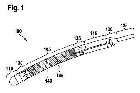
Fig. 1 shows a schematic view of a left ventricular assist system 100 with an
integrated line device
105 in accordance with one exemplary embodiment. The ventricular assist system
100 comprises
a cylindrically shaped, elongated structure with a substantially constant
outer diameter and
rounded, tapering ends for ease of placement by means of catheters in a blood
vessel, such as
the left ventricle or the aorta.
To begin with, the ventricular assist system 100 (here by way of example a
left ventricular assist
system 100 for percutaneous implantation into a left ventricle) comprises the
line device 105,
where in this case the line device 105 is arranged between a sensor head unit
110 and a motor
housing 115, an end unit 120 and a connecting cable 125 of the ventricular
assist system 100. In
this respect the line device can be connected to the sensor head unit 110 and
the motor housing
Date Recue/Date Received 2021-01-06
CA 03105915 2021-01-06
-10-
115 or, more specifically, the end unit 120 by means of one connecting element
130 and 135
each. The connecting elements 130 and 135 contain openings for receiving or
discharging the
blood. The coupling is effected, for example, by adhesive bonding. The line
device 105 and the
connecting element 130 can also consist of one part. That means that they can
be manufactured
in one piece. The sensor head unit 110 and the connecting element 130 in one
embodiment can
also be made of one part, i.e., in one piece.
The sensor head unit 110 of the ventricular assist system 100 comprises, for
example, a tip in the
form of a sensor assembly that is used, for example, for measuring the
pressure and/or the
temperature. The end unit 120 represents, for example, a proximal end of the
ventricular assist
system 100 and forms a transition between the motor housing 115 of the
ventricular assist system
100 and the connecting cable 125 for connecting the ventricular assist system
100 to an external
energy source or an external evaluating device or control device.
The line device 105 comprises a guide cannula 140 that comprises, at least
partially along a
direction of extent, a structure or, more specifically, a surface that is
structured here. For example,
the guide cannula 140 comprises a spiral-shaped surface structure. An
electrical conducting
element 145 is arranged inside the guide cannula 140, where in this case said
electrical
conducting element 145 is used for the electrical connection of the sensor
head unit 110 to the
connecting cable 125 at the proximal end of the ventricular assist system 100.
In accordance with one exemplary embodiment, the electrical conducting element
145 can
contain a meander, in order to achieve a length adjustment of the same. In
this case the meander
is placed preferably in the region of the motor housing 115.
Fig. 2 shows a schematic view of a sensor head unit 110 of a left ventricular
assist system 100 in
accordance with one exemplary embodiment.
The sensor head unit 110 of the ventricular assist system 100 comprises, for
example, a tip in the
form of a sensor assembly that is used, for example, for measuring the
pressure and/or the
temperature of a patient suffering from a heart disease. For this purpose the
sensor head unit 110
in accordance with one exemplary embodiment comprises two sensors 205 and a
signal
generator 210. The two sensors 205 may be, for example, a pressure sensor
and/or a
temperature sensor. The signal generator 210 can be, for example, an
ultrasonic element. In
Date Recue/Date Received 2021-01-06
CA 03105915 2021-01-06
- 11 -
accordance with one embodiment, both sensors 205 are arranged in a sensor
cavity 215, which is
filled with a potting compound for protecting the sensors 205 from blood
and/or mechanical
damage. Thus, this potting compound can be, for example, a solid and/or gel-
like silicone and/or a
silicone oil.
As shown in the schematic view of a sensor head unit 110 illustrated in this
embodiment, the
sensor head unit 110 is connected to the line device 105 by means of the
connecting element
130, where in this case the connecting element 130 comprises a plurality of
inlet windows 220,
through which the blood of the cardiac patient enters the ventricular assist
system.
Fig. 3 shows a schematic view of a sensor contact region 305 and a signal
generator contacting
region 310 of an electrical conducting element in accordance with one
exemplary embodiment.
In accordance with one exemplary embodiment, the electrical conducting element
comprises, for
example, a structure on at least one of its ends; said structure serves as a
sensor contact region
305 for directly mounting and/or contacting at least one sensor and/or as a
signal generator
contacting region 310 for contacting at least one signal generator by
conductive adhesive
bonding, soldering and/or bonding. In this case the sensor contact region 305
and the signal
generator contacting region 310 are arranged on the sensor head unit 110,
which is used, for
example, to measure the pressure and/or the temperature of a cardiac patient.
The sensor contact
region 305 is designed, for example, as a rectangular printed circuit board,
in order to receive
and/or to contact at least two sensors. Furthermore, the sensor contact region
comprises two
edges 315 and 320, where in this case the sensor contact region 305 can be
bent at these two
edges 315 and 320, in order to wrap around a groove 325 in the sensor head
unit 310. The signal
generator contacting region 310 is designed, for example, as a circular
printed circuit board, in
order to receive and/or to contact at least one signal generator, for example,
an ultrasonic
element. For this purpose the signal generator contacting region 310 in
accordance with one
exemplary embodiment comprises two bent contact points 330, in order to
contact the ultrasonic
element. Furthermore, the signal generator contacting region 310 also
comprises an edge 335, on
which it can be bent, in order to integrate itself in the cylindrical shape of
the ventricular assist
system in the best possible way.
Fig. 4 shows a three dimensional view of a sensor head unit 110 of a left
ventricular assist system
in accordance with one exemplary embodiment. The sensor head unit 110
comprises a sensor
Date Recue/Date Received 2021-01-06
CA 03105915 2021-01-06
- 12 -
head 405, which is formed, by way of example, in a mushroom shaped manner;
furthermore, the
sensor contact region 305, on which a sensor 205 is mounted; and finally the
connecting element
130, which comprises a plurality of inlet windows 220, through which the blood
of the cardiac
patient enters the ventricular assist system. Furthermore, a joining region
410 is provided that is
used to press fit the connecting element 130 to the sensor head unit 110. The
inlet windows 220
are defined by three webs 610, two of which are visible on the right side in
Fig. 4. In order to
minimize a possible pressure loss, the inlet windows are designed to be as
large as possible, so
that the thin webs 610 remain in the region 130. As shown in the schematic
view of a sensor head
unit 110 illustrated in this embodiment, the sensor head unit 110 is connected
in a fluid tight
manner to the line device 105 by means of the connecting element 130.
Fig. 5 shows a schematic view of a sensor head unit 110 of a left ventricular
assist system in
accordance with one exemplary embodiment. In accordance with one exemplary
embodiment, the
sensor head unit 110 comprises a sensor head 405, which is formed, by way of
example, in a
mushroom shaped manner; furthermore, the sensor contact region 305, on which
at least one
sensor is mounted and/or contacted; and, furthermore, the signal generator
contacting region 310,
on which at least one signal generator is contacted. A fitting of the sensor
contact region 305
and/or of the signal generator contacting region of the electrical conducting
element into the
sensor head unit 110 is shown in the schematic view of the sensor head unit
110 illustrated in this
embodiment, where in this case the sensor contact region 305 is bent at its at
least two edges, in
order to wrap around the groove 325 of the sensor head unit 110. Furthermore,
the signal
generator contacting region 310 is also bent at its edge, in order to
integrate itself in the cylindrical
shape of the ventricular assist system in the best possible way.
Fig. 6 shows a schematic view of a guide cannula 140 of a line device in
accordance with one
exemplary embodiment.
In accordance with one exemplary embodiment, the inlet cannula 140 is formed
as a type of
flexible cylindrical feed tube with a continuous, structured surface 605 for
guiding the electrical
conducting element. In this case the flexible guide cannula 140 is designed,
for example, as a
structure, which is cut out of a tube and which comprises a constant outer
diameter, where in this
case the cut pattern contains a continuous spiral 605 for supporting and
protecting the electrical
conducting element. Furthermore, the guide cannula comprises, for example, an
integrated
connecting element 130 consisting of a joining region 410 and a plurality of
webs 610 as a
Date Recue/Date Received 2021-01-06
CA 03105915 2021-01-06
- 13 -
transition region, with which the guide cannula 140 is integrally connected to
the connecting
element 130. In this respect the connecting element 130 is made, for example,
of the same
material as a metallic alloy. The region of the connecting element 130 between
the joining region
410 and the guide cannula forms the inlet windows, which are separated from
one another by thin
webs 610 (to which the electrical conducting element 145 can be guided) and
through which the
blood of the cardiac patient enters the ventricular assist system.
In an alternative exemplary embodiment of the guide cannula 140, the latter is
formed as a braid,
in which a flat strip is embedded, for example, as a support of the electrical
conducting element,
for the purpose of protecting the electrical conducting element. Said flat
strip can also comprise a
metallic alloy, for example, a nickel-titanium alloy.
Fig. 6B shows a schematic representation of a ventricular assist system 100
with a line device
105. The sensor head 110 and the guide cannula 140, which is made, for
example, of a NiTiNol
material and which comprises the connecting element 130 and the line device
105, can also be
seen in this embodiment. At the front in the region of the connecting element
130, the blood runs
between the webs 610 into the ventricular assist system 100 in the state
inserted in the patient.
For example, for manufacturing reasons, the connecting element 135 is designed
here as an
individual part. The motor housing 115 and the end unit 120 (which, for
example, can contain
contact pins, which are not shown in Fig. 6B and which are intended for
contacting a cable
through the body of the patient) are hermetically welded to one another or,
more specifically, are
connected to one another in a fluid tight manner at the rear of the motor
housing 112. The
electrical conducting element 145 is guided on the outside of the device or,
more specifically, the
guide cannula 140 from the tip of the sensor head 110 over the webs 610 of the
inlet cage or,
.. more specifically, the connecting element 130 and the spiral as part of the
guide cannula 140 to
the squirrel cage or, more specifically, to the additional connecting element
135, there over
another web 620, which corresponds to the web 610, then through the motor or,
more specifically,
the motor housing 115 as far as to the end unit 120, at which the electrical
conducting element
145 can then be electrically contacted with the line 125.
Fig. 7 shows a schematic view of a connection point element 705 of an
electrical conducting
element 145 in accordance with one exemplary embodiment.
Date Recue/Date Received 2021-01-06
CA 03105915 2021-01-06
- 14 -
In accordance with one exemplary embodiment, the electrical conducting element
145 comprises
the connection point element 705 on one of its ends. In this case the
connection point element
705 is formed, as an example, in a circular shape. However, in an alternative
exemplary
embodiment it can also be formed in an 0-shaped or U-shaped, hexagonal,
square, triangular or
generally polygonal shaped manner. Furthermore, in accordance with one
exemplary
embodiment, the connection point element 705 comprises a plurality of
connecting points 710,
which are arranged radially and/or circumferentially on an external
environment of the connection
point element 705. In this case the connecting points 710 are designed so as
to be round or
semicircular, so that a plurality of thin and flexible lines 715 of the
electrical conducting element
145 can be folded between the similarly radially arranged contact pins of a
feed-through element
(not shown), in order to be electrically contacted there by means of welding,
conductive adhesive
bonding and/or soldering.
Fig. 8 shows a schematic view of a contacted connection point element 705 of
an electrical
conducting element 145 in accordance with one exemplary embodiment at the
proximal end 120
of a ventricular assist system. In accordance with one exemplary embodiment,
the connection
point element 705, which is depicted, is a fully contacted connection point of
the electrical
conducting element 145. In this view the multilayer structure of the
electrical conducting element
145 is clearly visible. The connection point element 705 comprises a plurality
of semicircular
connecting points 710, which are arranged radially and/or circumferentially on
an external
environment of the connection point element 705. In this case each connecting
point 710 is
connected to one contact pin 805 each of a feed-through element (not shown) at
the proximal end
120 of the support system, where in this case the feed-through element is also
a conducting
element that is used to connect, for example, the power supply lines of the
electric motor 115 to
the supply cable 125. In this case the contacting of the electrical conducting
element 145 initially
at the metallic pins of the back end 120 enables a robust mechanical coupling
as a common
connecting element of the flexible conductors of the connecting cable 125 and
of the electrical
conducting element. A direct connection of the conductors of the connecting
cable to the electrical
conducting element is not to be recommended mechanically.
Fig. 9 shows a schematic cross-sectional view of an electrical conducting
element 145 in
accordance with one exemplary embodiment.
Date Recue/Date Received 2021-01-06
CA 03105915 2021-01-06
- 15 -
In accordance with one exemplary embodiment, the electrical conducting element
145 comprises
a plurality of coplanar layers 905 made of a conductive and/or insulating
material. In this case the
conductive layers comprise, by way of example, at least partially a gold
material; and the
insulating layers are made at least partially of a polyimide material.
Furthermore, the electrical
conducting element 145 also comprises a shielding element 910, which is
implemented, for
example, using the conductive layers and is based on a gold material. The
shielding element 910
has, for example, a width of 470 vin and a thickness of 10 m. As an
alternative to the exemplary
embodiment of a shielding element 910 shown in this embodiment, the shielding
element 910 can
also be implemented using a through-contacting between the individual layers.
In this case the
shielding element 910 is used to shield individual conductors or conductor
pairs of the electrical
connecting element, in order to prevent the occurrence of any electrical
and/or magnetic coupling
of fields into the lines of the electrical connecting element, in particular,
at higher frequencies, or
conversely to reduce the electromagnetic radiation from the electrical
connecting element. In
addition, the shielding can be used to adjust a specific wave resistance of
the electrical
connecting element and to reduce the influence of the environment for reasons
of high frequency
compatibility.
Furthermore, the electrical conducting element 145 comprises a plurality of
lines 715, where in
this case said lines 715 are arranged inside a layer and have, for example, a
width of 410 [im and
a thickness of 10 m. Thus, in accordance with one exemplary embodiment, the
electrical
conducting element 145 comprises four digital lines 915, which are arranged
outside the shielding
element 910, and, furthermore, two ultrasonic lines 920, which are arranged
inside the shielding
element 910.
.. Fig. 10 shows a flowchart of an exemplary embodiment of a method 1000 for
producing a line
device in accordance with one exemplary embodiment. In accordance with one
exemplary
embodiment, the method 1000 is carried out and/or triggered on a device 1010
for producing a
line device.
In a step 1020, a guide cannula and an electrical conducting element are
provided. In a step 1030
of the method 1000, the electrical conducting element is arranged inside the
guide cannula, in
order to produce a line device.
Date Recue/Date Received 2021-01-06
CA 03105915 2021-01-06
- 16 -
If an exemplary embodiment comprises an "and/or" conjunction between a first
feature and a
second feature, then such a conjunction should be understood to mean that the
exemplary
embodiment comprises both the first feature and the second feature in
accordance with one
embodiment and comprises either just the first feature or just the second
feature in accordance
with another embodiment.
Date Recue/Date Received 2021-01-06