Note: Descriptions are shown in the official language in which they were submitted.
TUNABLE LASER ASSEMBLY
FIELD OF THE INVENTION
[0001] This invention relates generally to tunable semiconductor lasers,
and more
particularly to the wavelength monitoring and control of tunable semiconductor
lasers.
BACKGROUND
[0002] Tunable lasers are critical components in many optical imaging
and optical
sensing systems. High output power, broad tuning, and extremely pure and
stable spectral
characteristics are required for high-performance systems. Vertical cavity
semiconductor
lasers (VCSELs) have proven to be good sources for these applications due to
their single-
frequency, mode-hop-free tuning characteristics which provide for long
coherence length
laser output. VCSELs differentiate themselves from other types of tunable
semiconductor
lasers in that the cavity length of the VCSEL is short enough that only one
longitudinal
mode under the gain curve is available for lasing. This is in comparison with
in-plane,
edge-emitting tunable lasers where multiple longitudinal modes exist under the
gain curve
requiring wavelength selective elements to select lasing only one longitudinal
mode. The
use of light-weight micro-electro-mechanical system (MEMS) tuning elements
enable
high-sweep rates e.g., 10 kHz to >1 MHz over broad tuning ranges e.g., 10 nm
to >100 nm.
VCSELs are also attractive because they are scalable to wafer-level
manufacturing and
therefore lower cost. Operating wavelengths can include a very wide range,
based only
upon the availability of semiconductor gain elements and optical Bragg grating
reflectors,
ranging from ultraviolet (UV), e.g., 250 nm out to many microns, e.g., > 5
microns.
[0003] Implementation of the optical imaging or optical sensing system
requires
accurate knowledge of the tunable laser wavelength as it sweeps over its
tuning range.
Many methods have been used to characterize the tunable laser wavelength,
including
multi-point calibration [1], built-in wavelength meters [2], bandpass filter
arrays [3],
wavelength discriminator arrays [4], wavelength-to-power calibration [5],
etalons [6, 7],
- 1 -
Date Recue/Date Received 2021-01-26
position sensitive detectors, [8], arrayed waveguide gratings [9] and a series
of fiber Bragg
gratings [10]. These methods acknowledge that the wavelength tuning
characteristics of
the tunable laser will vary over time responding to environmental (e.g.,
temperature,
pressure) and aging effects. There can also be short-term sweep-to-sweep
variations due
to inherent electro-mechanical properties of the tuning elements. Moreover,
instantaneous
characterization of wavelength becomes more difficult as the sweep rate
increases. Modern
optical imaging systems, for example such as those used in optical coherence
tomography
(OCT), employ interferometers to measure the instantaneous laser wavelength.
The output
from the interferometer interfaces with high-speed data acquisition system
enabling
compensation for any short-term variations in the laser spectral sweep
characteristics.
However, it is important that the overall spectral properties of the laser
output e.g., center
wavelength, optical bandwidth, and spectral shape, remain constant over the
operating
environment and lifetime of the laser. A typical approach for monitoring and
controlling
the center wavelength is to use a fiber bragg grating (FBG) with a single
reflection peak in
the vicinity of the center wavelength [11]. This provides a reference
wavelength that is
used as a `X-trigger' which often more stable for triggering the data
acquisition than an
electronic 'sweep trigger' (FIG. 1). One disadvantage of an FBG, in addition
to size and
cost, is that the FBG is not stable over temperature, it drifts with ¨ 10 pm/C
rate, which is
not desirable for a wavelength reference.
100041 The
optical output power from single-spatial mode tunable VCSELs is
limited by the small cavity size and thermal properties of the semiconductor
epitaxial layer
structure. Output power in the range of 50 mW or greater are required,
particularly to
achieve desired signal-to-noise sensitivity as the sweep rate increase to
speeds in excess of
>100 kHz. High output power from the tunable laser also reduces overall system
costs by
enabling lower cost components and assembly techniques downstream of the
tunable laser.
For these reasons, it is necessary to increase the output power from the VCSEL
using an
optical amplifier.
- 2 -
Date Recue/Date Received 2021-01-26
[0005] Low cost is also an essential element to enable optical imaging
and sensing
applications in higher volume consumer markets such as robotic machine vision,
autonomous driving, and home health care OCT applications.
[0006] The following novel concepts according to embodiments of the
present
invention provide a highly stable, low cost, tunable laser assembly based on
VCSELs,
semiconductor optical amplifiers and bulk optical components including optical
filters and
etalons. The concepts are applicable to both optically-pumped and electrically-
pumped
VC SELs
SUMMARY
[0007] To enable the wide-spread adoption of swept-source laser imaging,
Lidar,
and metrology applications in such areas as home health care OCT, autonomous
driving,
and robotic machine vision, the cost of the swept-source laser must be
significantly
reduced. The primary method for reducing cost in optoelectronic components is
through
optoelectronic integration of as many sub-components as possible on a common
packaging
platform. The majority of optoelectronic component cost is not in the
semiconductor chip
itself, but in the manufacturing process and sub-components that align, attach
and
ultimately couple light into the end-user optical fiber. Expensive
hermetically sealed,
temperature controlled, gold-plated packages must contain as many components
and
functions as possible to amortize the cost of the gold -plated packages and
thermo-electric
coolers (TECs).
100081 Integration of various optoelectronics components also presents
unique
challenges in terms of compromises in performance in order to achieve reduced
size and
cost. In the case of swept-source lasers, integrated wavelength monitoring
control
functions must be accomplished without introducing perturbation to the swept-
source laser
output spectrum that cause artifacts in the final system measurement and/or
image. OCT
imaging systems, for example, are sensitive to reflections in the optical path
that produce
parasitic etalons causing artifacts that are 50 dB or more below the main
signal.
- 3 -
Date Recue/Date Received 2021-01-26
[0009] One embodiment of the present invention provides a tunable laser
assembly
housed in a single enclosure wherein the center wavelength and tuning
bandwidth of the
tunable VCSEL is monitored with an optical configuration that does not
introduce
perturbation into the swept-source laser output spectrum that would cause an
artifact in the
OCT image.
100101 Integration of various optoelectronic components is constrained
by the size
requirements. Another embodiment of the present invention provides a tunable
laser
assembly housed in a single enclosure wherein the center wavelength and tuning
bandwidth
of the tunable VCSEL is monitored and the VCSEL chip, monitor photodiodes, and
temperature sensor all mounted on a common substrate.
[0011] Integration of various optoelectronics components in a small size
also brings
up the need for optical isolation between certain components to avoid
reflections that can
degrade performance or potentially damage the laser. Another embodiment of the
present
invention provides a tunable laser assembly housed in a single enclosure
wherein optical
isolation is achieved without employing a non-reciprocal, faraday-effect
material.
[0012] One embodiment of the present invention provides a tunable laser
assembly
including: a tunable semiconductor laser chip emitting tunable laser
radiation; a beam
splitter; at least one wavelength monitoring optical element; at least one
photodetector; a
semiconductor optical amplifier; and at least one optical isolator; wherein
the tunable
semiconductor laser chip, the beam splitter, the at least one wavelength
monitoring optical
element, the at least one photodetector, the semiconductor amplifier, and the
at least one
optical isolator are mounted on a common baseplate; and wherein the at least
one
wavelength monitoring element generates a signal that is used to monitor and
control at
least one of the absolute wavelength and optical bandwidth of said tunable
laser radiation.
100131 One embodiment of the present invention provides a method for
controlling
the center wavelength and the optical bandwidth of swept-source tunable laser
that using
the timing information from a signal generated by a reference optical
wavelength filter and
- 4 -
Date Recue/Date Received 2021-01-26
an optical element that generates signal pulses corresponding to nearly
equally spaced
wavenumbers.
[0014] One embodiment of the present invention provides a stabilized
laser
including: a tunable semiconductor laser chip emitting tunable laser
radiation; a beam
splitter; at least one wavelength monitoring optical element; at least one
photodetector; a
semiconductor optical amplifier; at least one optical isolator; and a closed
loop controller;
wherein the tunable semiconductor laser chip, the beam splitter, the at least
one wavelength
monitoring optical element, the at least one photodetector, the semiconductor
amplifier,
and the at least one optical isolator are mounted on a common baseplate; and
wherein the
at least one wavelength monitoring optical element generates a signal that is
input to the
closed-loop controller and the closed-loop controller stabilizes the absolute
wavelength and
optical bandwidth of said tunable laser radiation.
100151 One embodiment of the present invention provides a swept source
optical
coherence tomography system including: a stabilized laser including: a tunable
semiconductor laser chip emitting tunable laser radiation; a beam splitter; at
least one
wavelength monitoring optical element; at least one photodetector; a
semiconductor optical
amplifier; at least one optical isolator; and a closed loop controller;
wherein the tunable
semiconductor laser chip, the beam splitter, the at least one wavelength
monitoring optical
element, the at least one photodetector, the semiconductor amplifier, and the
at least one
optical isolator are mounted on a common baseplate; and wherein the at least
one
wavelength monitoring optical element generates a signal that is input to the
closed-loop
controller and the closed-loop controller stabilizes the absolute wavelength
and optical
bandwidth of said tunable laser radiation; an optical coherence tomography
(OCT)
interferometer; and an OCT detector; wherein at least a portion of the said
tunable laser
radiation is directed to the OCT interferometer and the output of the OCT
interferometer
directed to an OCT detector for generating OCT interferograms.
- 5 -
Date Recue/Date Received 2021-01-26
BRIEF DESCRIPTION OF THE DRAWINGS
[0016]
Figure 1 is block diagram of tunable laser assembly according to prior art
with fiber bragg grating based center wavelength monitoring.
[0017]
Figure 2 is schematic diagram of highly stable, low cost, tunable laser
assembly design according to an embodiment of the present invention.
100181
Figure 3 shows the optical configuration and considerations for determining
the dimensions of the beam splitter component.
[0019]
Figure 4 shows a tunable laser assembly design according to another
embodiment of the present invention.
100201
Figure 5 shows a tunable laser assembly design according to another
embodiment of the present invention.
[0021]
Figure 6 shows a tunable laser assembly design according to another
embodiment of the present invention.
100221
Figure 7 shows a tunable laser assembly design according to another
embodiment of the present invention.
[0023]
Figure 8 shows a tunable laser assembly design according to another
embodiment of the present invention.
100241
Figure 9 shows a tunable laser assembly design according to another
embodiment of the present invention.
[0025]
Figure 10 shows a graph of sweep trajectories according to an embodiment.
100261 Figure 11 shows a measure of the time required for the device to move
from
a starting wavenumber to an ending wavenumber according to an embodiment.
[0027] Figures 12A and 12B show the operation of a MEMS-VCSEL without and
with optical bandwidth control respectively.
100281
Figure 13 is a schematic diagram of a highly-stable tunable laser with a
closed-loop controller according to an embodiment of the present invention.
[0029] Figures 14A and 14B are schematic diagrams of example swept source OCT
systems.
- 6 -
Date Recue/Date Received 2021-01-26
DETAILED DESCRIPTION OF THE PREFERRED EMBODIMENTS
[0030] The description of illustrative embodiments according to
principles of the
present invention is intended to be read in connection with the accompanying
drawings,
which are to be considered part of the entire written description. In the
description of
embodiments of the invention disclosed herein, any reference to direction or
orientation is
merely intended for convenience of description and is not intended in any way
to limit the
scope of the present invention. Relative terms such as "lower," "upper,"
"horizontal,"
"vertical," "above," "below," "up," "down," "top" and "bottom" as well as
derivative
thereof (e.g., "horizontally," "downwardly," "upwardly," etc.) should be
construed to refer
to the orientation as then described or as shown in the drawing under
discussion. These
relative terms are for convenience of description only and do not require that
the apparatus
be constructed or operated in a particular orientation unless explicitly
indicated as such.
Terms such as "attached," "affixed," "connected," "coupled," "interconnected,"
and
similar refer to a relationship wherein structures are secured or attached to
one another
either directly or indirectly through intervening structures, as well as both
movable or rigid
attachments or relationships, unless expressly described otherwise. Moreover,
the features
and benefits of the invention are illustrated by reference to the exemplified
embodiments.
Accordingly, the invention expressly should not be limited to such exemplary
embodiments illustrating some possible non-limiting combination of features
that may
exist alone or in other combinations of features; the scope of the invention
being defined
by the claims appended hereto.
[0031] This disclosure describes the best mode or modes of practicing
the invention
as presently contemplated. This description is not intended to be understood
in a limiting
sense, but provides an example of the invention presented solely for
illustrative purposes
by reference to the accompanying drawings to advise one of ordinary skill in
the art of the
advantages and construction of the invention. Although some elements disclosed
herein
are implemented on a chip or chipset without loss of generality, it is
understood that many
- 7 -
Date Recue/Date Received 2021-01-26
of these elements may also be implemented, for example, on one or more chips
and/or one
or more optical elements. In the various views of the drawings, like reference
characters
designate like or similar parts.
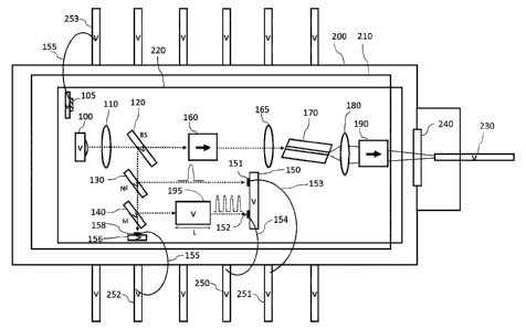
[0032] FIG. 2 is a schematic of a tunable laser assembly incorporating a
tunable
VCSEL chip, semiconductor amplifier chip and wavelength monitoring components
all
mounted to a common baseplate 220. The temperature of the baseplate is
maintained
through a feedback loop comprising a thermo-electric cooler (TEC) 210 and a
temperature
sensor 105 attached to the baseplate and connected to the external control
circuit by an
electrical connection 155 to an external package pin 253. As shown in FIG. 2,
a tunable
laser assembly according to an embodiment of the present invention includes an
enclosure
200 containing a tunable VCSEL chip 100 and semiconductor optical amplifier
(SOA) chip
170. Laser radiation from the tunable VCSEL is coupled into the SOA input
waveguide
via the collimating lens 110 and focusing lens 165. An optical isolator 160 is
inserted
between the VCSEL and SOA to prevent backwards propagating laser radiation
from the
SOA (e.g., amplified spontaneous emission (ASE) and/or amplified reflected
signal) from
setting up a potential laser cavity between the SOA and the top mirror on the
tunable
VCSEL chip. The amplified laser radiation from SOA output waveguide propagates
through optical lens 180, through the window in the enclosure wall 240 and is
coupled into
the optical output fiber 230. An output optical isolator 190 is inserted
between the SOA
output and the optical fiber to prevent reflections from the optical fiber and
components
downstream of the optical from propagating back to the SOA.
100331 In order to monitor both the absolute wavelength and the
bandwidth of the
tunable optical spectrum, two optical monitoring paths are provided that
include
wavelength monitoring optical elements comprised of a notch filter 130 and
etalon 195. A
beam splitter 120 directs a portion of the laser radiation from the tunable
VCSEL so that it
is incident on notch filter (NF) 130 at an angle. The majority of the tunable
optical
spectrum is transmitted through the notch filter, except for a narrow band
that is reflected
and made incident on a photodetector 151. The signal from photodetector 151 is
connected
- 8 -
Date Recue/Date Received 2021-01-26
to an external absolute wavelength monitor circuit by an electrical connection
153 to an
external package pin 251. The absolute wavelength is determined by reference
to the
narrow band notch reflection profile which can be calibrated against an
external source.
By holding the relative timing of the photo-detected narrow-band notch
reflection profile
relative to a known timing reference such as the electronic sweep trigger, the
absolute
wavelength of a specific portion of the tunable optical spectrum (e.g., the
center
wavelength) can be held constant in time relative to the trigger. The
temperature
dependence of the narrow-band notch reflection profile is minimized by TEC
control of
the baseplate temperature. Those skilled in the art will understand that
control of the center
wavelength doesn't mean that the exact center wavelength must be monitored,
any portion
of the tunable laser spectrum can used for the reference, although those
wavelengths near
the center are preferred as there is larger control signal. Those skilled in
the art will also
recognize that several methods exist for creating notch filters, that is, a
filter that transmits
the majority of its specified wavelength spectrum and highly reflects a narrow-
band portion
of the spectrum. Bragg grating are the most prevalent design for notch filters
and can be
implemented using conventional dielectric thin-film deposition or holographic
techniques
such as in Volume Holographic Gratings (VHG), which are also known as Volume
Bragg
Gratings (VBG). The optical-fiber version of a notch filter, a fiber Bragg
gratings (FBG),
has often been used in tunable lasers to provide an absolute wavelength
reference for
trigger/controlling the sweep. The advantage of the free-space notch filter in
the present
embodiments compared to an FBG, is the smaller size, compatibility with free-
space
integration, and the fact that it is temperature controlled simply by being
mounted on the
common baseplate with the other optical components. It is more difficult,
bulky and
expensive to temperature stabilize an FBG.
100341 To
monitor the bandwidth of the tunable optical spectrum (the 'optical
bandwidth', or `bandwidth'), the optical signal that is transmitted through
the notch filter
130 is made incident at an angle on a partially-reflecting mirror (M) 140. The
reflected
signal from the mirror propagates through etalon 195, having a physical length
L, and is
- 9 -
Date Recue/Date Received 2021-01-26
made incident on a photodetector 152. The signal from photodetector 152 is
connected to
an external optical bandwidth monitor circuit by an electrical connection 154
to an external
package pin 250. As the tunable VCSEL sweeps over the optical spectrum, the
output
signal from photodetector 152 consists of a series of pulses with the optical
frequency
spacing (Af) between the adjacent maxima determined by the free spectral range
(FSR) of
the etalon: Af = c/2nL, where c is the speed of light in vacuum and n is the
index of
refraction of the etalon. The corresponding wavelength spacing (AX) is given
by
AX, = 22/2nL, which is not constant but varies as the laser tunes. For a
tunable laser
operating with a center wavelength of 1300nm, the approximate wavelength
spacing for an
etalon made out of BK-7 glass (n = 1.5) and having L = 2.0 mm is 0.28 nm. Thus
the series
of pulses generated by the etalon provides a means to measure the bandwidth of
the optical
signal with a resolution determined by the FSR of the etalon. By controlling
the timing of
a defined number of pulses that occur relative to a known reference such as
the internal
sweep trigger or the absolute wavelength reference from the narrow-band notch
filter
reflection profile, the external circuit can control and hold constant the
optical bandwidth
of the tunable laser. Other materials that have higher refractive index than
glass, such as
LiNb03, GaAs, Si, or InP can be used for the etalon and have the advantage of
more
compact size and higher fringe contrast.
[0035] In
addition to monitoring the absolute wavelength and the bandwidth of the
tunable optical spectrum, it is also desirable to monitor the output power
from the tunable
VCSEL. A signal proportional to the optical output power can be obtained from
etalon-
generated signal from photodetector 152. However, to obtain a signal that is
not distorted
by the etalon, a partially-reflecting mirror 140, as shown in FIG. 2,
transmits the full optical
spectrum, minus the narrow-band notch reflection profile, to a photodetector
158. The
signal from photodetector 158 is connected to an external optical bandwidth
monitor circuit
by an electrical connection 155 to an external package pin 252. In this
embodiment,
individual photodetectors 151 and 152 are shown mounted on a common substrate
150,
- 10 -
Date Recue/Date Received 2021-01-26
whereas photodetector 158 is shown mounted individually on substrate 156.
Those skilled
in the art recognize that these drawings are only illustrative and many
configurations of
photodetectors exist, for example 151 and 152 could be a 2-element monolithic
photodetector array mounted on a substrate, or all three photodetectors 151,
152, and 158
could be a 3-element array mounted on a substrate, or all three photodetectors
151, 152,
and 158 could be individual photodetectors mounted on individual substrates.
[0036] The
wavelength monitoring optical elements must be designed to prevent
introducing reflections in the optical path that create perturbations in the
wavelength tuning
spectrum. Any multiple propagation paths in the optical beam that make their
way into the
laser output signal will appear as artifacts in any OCT imaging system. The
beam splitter
120 is particularly sensitive component as it is placed directly in the main
laser beam
optical path. In order to prevent multi-path reflections from the beam
splitter, the beam
splitter thickness must be large enough to prevent secondary reflections
within the beam
splitter from coupling into the laser output signal. In the embodiment shown
in FIG. 3, the
thickness, d, of the beam splitter 120 is chosen so that the secondary
reflected beam 122
that is parallel with the main optical beam 121 has a large enough offset, 0,
that it does not
effectively couple into SOA 170 because it arrives at the SOA input at an
angle. For
example, taking the beam splitter to be BK7 glass (n = 1.5) and assuming a
propagating
collimated gaussian beam having a mode field radius of approximately 170 um, a
thickness
of d = 0.75 mm or greater will provide more than 50dB rejection of the
secondary beam
coupling into the SOA amplifier chip. Secondary reflections from the beam
splitter also
can propagate into the wavelength monitoring circuit and distort the
wavelength
monitoring signals. The beam splitter thickness must be chosen so that the
secondary beam
offsets, p and q, are large enough so that the secondary beam does not add
unwanted
interference to the primary beam ¨ either in the forward transmission or for
detection by
the wavelength monitoring photodetectors 151 and 152. A beam splitter
thickness greater
than or equal to 0.75mm is required to take advantage of readily available
optical
components to construct a practical design; such a thickness in BK7 glass can
create a
- 11 -
Date Recue/Date Received 2021-01-26
beam offset of approximately 570um which can readily suppress cross coupling
between
the primary and secondary beams to below -50dB with a suitable choice for the
collimation
lens 110.
[0037] In another embodiment of the present invention, shown in FIG. 4,
a quarter-
wave polarization waveplate 300 and polarizer 310 are inserted between the
VCSEL 100
and SOA 170 to prevent backwards propagating laser radiation from the SOA
(e.g.,
amplified spontaneous emission (ASE) and/or amplified reflected signal) from
setting up
a potential laser cavity between the SOA and the top mirror on the tunable
VCSEL chip.
This combination of polarizer and quarter-wave polarization waveplate, which
converts the
linear polarized output light from the VCSEL to circular polarization,
introduces a 3-dB
loss in output power. However, it provides optical isolation between the SOA
and VCSEL
without the need for a Faraday rotator material, which is often expensive and
can have high
optical loss.
100381 In another embodiment of the present invention, shown in FIG. 5,
the optical
isolator 160 is inserted in between the VCSEL 100 and the beam splitter 120.
The
advantage of this configuration is that, in addition to providing optical
isolation between
the VCSEL and SOA, the isolator reduces the effect of back-reflections from
the
wavelength monitoring components: filter, etalon, and photodetectors, from
perturbing the
VCSEL and generating artifacts.
[0039] In another embodiment of the present invention, shown in FIG. 6,
a quarter-
wave polarization waveplate 300 and polarizer 310 are inserted between the
VCSEL 100
and beam splitter 120. The advantage of this configuration is that, in
addition to providing
optical isolation between the SOA and VCSEL, the quarter-wave polarization
waveplate/polarizer combination reduces the effect of back-reflections from
the
wavelength monitoring components: filter, etalon, and photodetectors, from
perturbing the
VCSEL and generating artifacts. This combination of polarizer and quarter-wave
polarization waveplate, which converts the linear polarized output light from
the VCSEL
to circular polarization, introduces a 3-dB loss in output power. However, it
provides
- 12 -
Date Recue/Date Received 2021-01-26
optical isolation without the need for a Faraday rotator material, which is
often expensive
and can have high optical loss.
[0040] In
another embodiment of the present invention, shown in FIG. 7, the notch
filter 130 is replaced with a bandpass filter 430. The bandpass filter
operates in
transmission mode to generate the optical pulse used for center wavelength
control, as
compared to the notch filter which typically operates in reflection mode. The
beam splitter
120 directs a portion of the laser radiation from the tunable VCSEL so that it
is incident on
a partially reflecting mirror (M) 440 at an angle. The mirror 440 reflects a
portion of the
laser radiation through an etalon 195 and is made incident on a photodetector
452. The
signal from photodetector 452 is connected to an external optical bandwidth
monitor circuit
by an electrical connection 454 to an external package pin 460. The mirror
transmits the
remainder of the laser radiation through bandpass filter 430. The majority of
the tunable
optical spectrum is reflected or absorbed the bandpass filter, except for a
narrow band that
is transmitted and made incident on a photodetector 451. The signal from
photodetector
451 is connected to an external absolute wavelength monitor circuit by an
electrical
connection 453 to an external package pin 461. The absolute wavelength is
determined by
reference to the narrow bandpass transmission profile which can be calibrated
against an
external source. By holding the relative timing of the photo-detected bandpass
transmission profile relative to a known timing reference such as the sweep
trigger
generator, the absolute wavelength of a specific portion of the tunable
optical spectrum
(e.g., the center wavelength) can be held constant in time. The temperature
dependence of
the bandpass filter transmission profile is minimized by TEC control of the
baseplate 220
temperature. Those skilled in the art will recognize that several methods
exist for creating
narrow optical bandpass filters, that is, a filter that reflects or absorbs
the majority of its
specified wavelength spectrum and transmits only a narrow-band portion of the
spectrum.
Multi-layer dielectric filters designed with coupled Fabry-Perot cavities are
a common
design, with bandpass filter shape that can be tailored by the selection of
the number of
Fabry-Perot cavities. The exact shape of the bandpass filter depends on many
factors such
- 13 -
Date Recue/Date Received 2021-01-26
as the laser sweep rate, bandwidth of the detection electronics, and allowed
electrical jitter
requirements for the generated trigger signal. The faster the transition rate
of the electrical
signal generated by detecting the laser tuning signal as it sweeps through the
edge of the
bandpass filter, or notch filter, the lower the jitter on the trigger signal.
For a laser sweeping
at a constant rate over a 100 nm optical bandwidth with a 100 kHz repetition
rate and 70%
duty cycle, a bandpass filter having a bandwidth of 1 nm @ FWHM and 10 nm @ -
20 dB
will generate a center wavelength pulse with a transition time of 4.5nm *
(7u5/100nm) =
315 ns. To keep the trigger jitter below 20 pm peak-to-peak, the optical
filter must have
sharp rolloff on the filter edge, which can be achieved with a filter have a
bandwidth of 0.5
nm (FWEIM) and 1 nm full-width @ -20 dB. For a bandpass filter, the bandwidth
is the
transmission bandwidth, for a notch filter, the bandwidth is the reflection
bandwidth.
[0041] In
another embodiment of the present invention, shown in FIG. 8, the out-
of-band reflection from the bandpass filter 630 provides the signal that is
incident on the
etalon 195 and used for bandwidth monitoring. The beam splitter 120 directs a
portion of
the laser radiation from the tunable VC SEL so that it is incident on bandpass
filter 630. A
narrow-band spectrum of the laser radiation is transmitted through the
bandpass filter and
is made incident on a photodetector 151. The signal from photodetector 151 is
connected
to an external absolute wavelength monitor circuit by an electrical connection
653 to an
external package pin 654. The absolute wavelength is determined by reference
to the
narrow bandpass transmission profile which can be calibrated against an
external source.
The bandpass filter is designed so that the majority of the tunable laser
radiation spectrum
is reflected from the bandpass filter. This reflected signal passes back
through the beam
splitter 120 and passes through etalon 195 and is made incident on a
photodetector 152.
The signal from photodetector 152 is connected to an external optical
bandwidth monitor
circuit by an electrical connection 154 to an external package pin 253. In
this compact
embodiment, turning mirrors 640 and 645 enable the photodetectors 151 and 152,
the
VCSEL chip, and the temperature sensor 340 to be attached to a common
substrate 330.
Those skilled in the art will recognize that other optical configurations are
possible that do
- 14 -
Date Recue/Date Received 2021-01-26
not use turning mirrors and where the photodetectors, VCSEL chip and
temperature sensor
do not share a common substrate.
[0042] In another embodiment of the present invention, shown in FIG. 9,
the tunable
VCSEL chip 700 is optically pumped by the pump laser 710. The pump radiation
is
directed to the VCSEL chip via the dichroic mirror (DM) 720, which is
substantially
reflecting at the pump wavelength (e.g., 780nm, 850nm, 980 nm, 1300 nm) but
transmits
the broadband VCSEL signal wavelengths (e.g., 1000-1100m, 1250-1350 nm, 1450-
1600
nm). The dichroic mirror is located between the VCSEL chip 700 and the beam
splitter
120 that taps off a portion of the tunable laser radiation in order to
implement the optical
wavelength monitoring functions. Those skilled in the art will recognize that
other optical
configurations are possible, for example, the beam splitter could be located
between the
VCSEL chip and the dichroic mirror. Alternatively, the VCSEL chip could be
optically
pumped from the backside of the chip, eliminating the need for the dichroic
mirror. It is
well known that the quality of the tunable laser emission depends on the
quality of the
pump laser. For demanding applications such as OCT, the pump laser needs to be
a single-
frequency laser such as a distributed feedback (DFB), distributed Bragg
reflector (DBR),
Y-branch, or other external cavity laser such a volume holographic grating
(VHG)
stabilized laser.
[0043] There are several possible methods to use the signals generated
by the
notch/bandpass filter and etalon to control the absolute wavelength (center
wavelength)
and tuning optical bandwidth, respectively. Open loop operation of a MEMS-
VCSEL
swept laser source presents many challenges in maintaining a stable output
over long
operating time frames and/or changing environmental conditions. Long term
charging
effects in the MEMS structure lead to changes in the effective voltage that is
applied to the
device. As the MEMS structure is an electrostatically controlled moving
membrane the
relationship between the voltage on the electrodes and the mirror position is
highly non-
linear. Slight changes in operating DC level can result in large changes to
the sweep profile
and ultimately the overall bandwidth that is contained within a given time
window.
- 15 -
Date Recue/Date Received 2021-01-26
Additionally, the mechanical damping of the device is highly sensitive to the
surrounding
environment. Open-loop calibration/corrections can be applied, but these
require extensive
production characterization procedures and long-term testing.
[0044] To enable robust and long-term operation it is desired that an
optical
reference signal be used to monitor and subsequently control the high voltage
drive signals
to the tunable MEMS-element such that the swept bandwidth is maintained under
all
operating conditions and timeframes. This optical signal is used to generate
timing
information which has a direct correlation to the optical bandwidth and
overall sweep
trajectory. The typical mechanism for bandwidth loss or gain is mainly that
the sweep
velocity changes, as illustrated in FIG. 10. As the defined active sweep
period is typically
fixed by other system parameters, any shift in the sweep velocity directly
results in a change
in the overall sweep bandwidth within a given time window. Under this
assumption, it can
be shown that controlling the time difference (t2-t1 in FIG. 10) required to
sweep a defined
bandwidth (lambda2-lambdal in FIG. 10) is sufficient to maintaining the
overall
bandwidth of the tunable swept-source MEMS-VCSEL.
[0045] An optical etalon can be used to generate electrical pulses (via
zero crossing
detection) each of which corresponds to nearly equally spaced wavenumbers. An
electronic
counter circuit can then be used to generate a measure of the time (deltaT)
required for the
device to move from a starting wavenumber to an ending wavenumber, as shown in
FIG.
11. The counter electronics combined with the etalon allow a very fine
resolution and
adjustable timing "marker" to be placed at an ideal location within the sweep
trajectory by
selecting a programmable 'Nth' pulse as the control marker. This
implementation for
marking the sweep end-point is highly advantageous compared to using fixed
wavelength
references (notch filter, bandpass filter) which are not flexible enough to
select a proper
end-point for all MEMS-VCSEL devices, due to variation in absolute sweep
wavelength,
difference in sweep rates, and/or different bandwidth requirements. For
ensuring absolute
wavelength accuracy, the timer starting point (ti, lambdal) is generated by
the Reference
2-Filter (i.e. the notch or bandpass filter) while the second timing marker
(t2) is generated
- 16 -
Date Recue/Date Received 2021-01-26
by the etalon, selecting the appropriate 'Nth' pulse to use for bandwidth
control. The deltaT
generated by the counter electronics 1320 may be used as feedback in a
proportional-
integral-derivative control algorithm (ND) to implement a closed-loop
controller 1300, as
shown in FIG. 13. The MD 1310 measures the difference between the deltaT and a
reference time corresponding to the desired bandwidth (refT) Tuning
coefficients are
applied to this difference generating a MD output that adjusts the gain 1340
of the high
voltage signal 1330 driving the MEMS-VCSEL 1360 in the tunable laser assembly
1350.
This minimizes the difference between deltaT and refT, maintaining the desired
optical
bandwidth. This same method can be applied for use in any type of tunable
swept source
laser and is not limited to the integrated optical assembly embodiments in
this disclosure.
For example, an FBG can be used as the Reference k-Filter and a Mach-Zehnder
Interferometer (MZI) or FBG having multiple reflection peaks may be used in a
similar
manner as the etalon to obtain the same timing information for the follow-on
control
algorithms.
100461 The application of the optical bandwidth control method described
in the
preceding sections is demonstrated in FIGS. 12A and 12B, which show operation
of a
MEMS VCSEL without and with bandwidth control. Without bandwidth control,
there is
a change in bandwidth of approximately -5% over 20 hours as the DC bias
operating point
slowly drifts (FIG. 12A). This change in bandwidth is eliminated with
bandwidth control
method engaged (FIG. 12B).
[0047] Optical Coherence Tomography (OCT) is a non-invasive,
interferometric
optical imaging technique that can generate micron resolution 2D and 3D images
of tissue
and other scattering or reflective materials. With applications in medicine,
biological
research, industrial inspection, metrology, and quality assurance, OCT can be
used for
subsurface imaging, surface profiling, motion characterization, fluid flow
characterization,
index of refraction measurement, birefringence characterization, scattering
characterization, distance measurement, and measurement of dynamic processes.
The most
common implementation of OCT is spectral! Fourier domain OCT (SD-OCT), which
uses
- 17 -
Date Recue/Date Received 2021-01-26
a broadband light source, interferometer, and spectrometer. An alternate
implementation
of OCT is swept source OCT (SS-OCT). SS-OCT uses a tunable laser (sometimes
called
a wavelength swept laser), interferometer, OCT detector, and high speed analog
to digital
(A/D) converter. The tunable laser sweeps an emission wavelength in time which
is used
as input to an OCT interferometer. An OCT interferogram is formed by
interfering and
detecting light from a sample arm with light from a reference arm in the OCT
interferometer, which is detected by the OCT detector and digitized by the A/D
converter.
Processing the digitized interferogram generates a reflectivity vs. depth
profile of the
sample, called an A-scan. Multiple A-scans can be obtained to generate two
dimensional
OCT images or three dimensional OCT volumes.
[0048] FIGS. 14A and 14B show schematic diagrams of example swept source OCT
systems. Depending on the wavelength of operation, a coupler based or combined
coupler
and circulator based interferometer might be preferred. FIG. 14A shows a swept
source
OCT system 1400 in which light from a tunable laser 1405 is directed to a
coupler 1410
which splits light between a sample path 1415 and a reference path 1420. Light
from the
sample path 1415 and light from the reference path 1420 are combined at a path
interfering
element 1425 and directed to an OCT detector 1430. The electrical signal from
the OCT
detector 1430 is digitized by the A/D converter 1435. FIG. 14B shows a swept
source
OCT system 1450 in which light from a tunable laser 1455 is directed to a
coupler 1460
which splits light between a sample path 1465 including an optical circulator
1467 and a
reference path 1470 including an optical circulator 1472. Light from the
sample path 1465
and light from the reference path 1470 are combined at a path interfering
element 1475 and
directed to an OCT detector 1480. The electrical signal from the OCT detector
1480 is
digitized by the A/D converter 1485. While FIG. 14 shows common OCT system
topologies, other OCT system topologies are possible including using various
combinations of couplers and optical circulators not shown in FIG 14.
Components in a
SS-OCT system may be any one of or any combination of fiber optic components,
free
space components, photonic integrated circuits (PIC), and planar lightwave
circuits (PLC).
- 18 -
Date Recue/Date Received 2021-01-26
[0049] The present invention has been described at some length and with
some
particularity with respect to the several described embodiments, it is not
intended that it
should be limited to any such particulars or embodiments or any particular
embodiment,
but it is to be construed with references to the appended claims so as to
provide the broadest
possible interpretation of such claims in view of the prior art and,
therefore, to effectively
encompass the intended scope of the invention. Furthermore, the foregoing
describes the
invention in terms of embodiments foreseen by the inventor for which an
enabling
description was available, notwithstanding that insubstantial modifications of
the
invention, not presently foreseen, may nonetheless represent equivalents
thereto.
100501 References:
[1] US 6,362,878 Bl, Wang, "Multipoint Wavelength Calibration Technique".
[2] Keysight Technologies, Data Sheet, 5988-8518EN, December 2017.
[3] US 6,486,984 Bl, Baney, "Wavelength Monitor Using Hybrid Approach".
[4] US 5,850,292, Braun, "Wavelength Monitor for Optical Signals".
[5] US 6,043,883, Leckel, "Wavemeter and an Arrangement for the Adjustment of
the Wavelength of the Signals of an Optical Source".
[6] H. Nasu, 'Wavelength Monitor Integrated Laser Modules for 25-GHz Spacing
Tunable Applications", IEEE I Set. Topics Quantum Electron., Vol. 11, No. 1,
2005, pp.
157- 164.
[7] US 6,498,800 B 1 , Watterson, "Double Etalon Optical Wavelength Reference
Device".
[8] US 6,594,022 Bl, Watterson, "Wavelength Reference Device".
- 19 -
Date Recue/Date Received 2021-01-26
[9] R. Yu, "Rapid High-Precision In Situ Wavelength Calibration for Tunable
Lasers Using an Athermal AWG and a PD Array", IEEE Photon. Technol. Lett.,
Vol. 24,
No. 1, 2012, pp. 70-72.
[10] US 5,982,791, Sorin, "Wavelength Tracking in Adjustable Optical Systems".
[11] SL10 and SL13 Series MEMS-VCSEL Swept Sources ¨ User Manual,
www.thorlabs.com
- 20 -
Date Recue/Date Received 2021-01-26