Note: Descriptions are shown in the official language in which they were submitted.
CA 03107510 2021-01-25
SIGNAL TRANSMISSION METHOD, NETWORK DEVICE AND
TERMINAL DEVICE
TECHNICAL FIELD
[0001] Embodiments of the present application relate to the field of
communication, and
specifically, to a signal transmission method, a network device, and a
terminal device.
BACKGROUND
[0002] With the evolution of communication systems, higher requirements
have been
proposed for terminal power saving. For example, for the existing
Discontinuous Reception
(DRX) mechanism, in each On Duration, a terminal needs to continuously detect
Physical
Downlink Control Channel (PDCCH) to determine whether a base station schedules
data
transmission that sends to itself. However, for most terminals, there may be
no need to
receive data transmission for a long time, but it is still necessary to
maintain a regular wake
up mechanism to monitor possible downlink transmissions. For such terminals,
there is room
for further optimization of power saving. The situation is similar to a
terminal receiving a
paging message in an idle state.
[0003] For the DRX mechanism, an indication signal may be sent to the
terminal before
the On Duration, and the terminal performs PDCCH detection and data reception
in the On
Duration of the DRX only after the indication signal has been detected;
otherwise, the
PDCCH detection is not performed. The indication signal is a Wake-up Signal
(WUS), and
the Wake-up Signal is also called a power saving signal. Similarly, for the
terminal receiving
the paging message in the idle state, before a Paging Occasion (PO), whether
the PDCCH
needs to be detected at this PO is determined by detecting the power saving
signal.
Date Recue/Date Received 2021-01-26
CA 03107510 2021-01-25
[0004] In a case of introducing Bandwidth Part (BWP), there is currently no
clear
solution as to how to configure the power saving signal.
SUMMARY
[0005] The embodiments of the present application provide a signal
transmission method,
a network device, and a terminal device, which is beneficial to improve the
flexibility of the
terminal device to receive a power saving signal, thereby a better power
saving gain can be
realized.
[0006] In a first aspect, a signal transmission method is provided. The
method includes:
sending, by a network device if a terminal device is configured with multiple
Bandwidth
Parts (BWPs), configuration information of each BWP's corresponding power
saving signal
of the multiple BWPs to the terminal device.
[0007] In a second aspect, a signal transmission method is provided. The
method
includes: receiving, by a terminal device if the terminal device is configured
with multiple
Bandwidth Parts (BWPs), configuration information of each BWP's corresponding
power
saving signal of the multiple BWPs sent by a network device.
[0008] In a third aspect, a network device is provided for performing
methods in the first
aspect or various implementations thereof described above.
[0009] Specifically, the network device includes function modules for
performing the
methods in the first aspect or various implementations thereof described
above.
[0010] In a fourth aspect, a terminal device is provided for performing
methods in the
second aspect or various implementations thereof described above.
[0011] Specifically, the terminal device includes function modules for
performing the
methods in the second aspect or various implementations thereof described
above.
[0012] In a fifth aspect, a network device is provided, including a
processor and a
memory. The memory is configured to store a computer program, and the
processor is
2
Date Recue/Date Received 2021-01-26
CA 03107510 2021-01-25
configured to invoke and run the computer program stored in the memory, and
execute
methods in the first aspect or various implementations thereof described
above.
[0013] According to a sixth aspect, a terminal device is provided,
including a processor
and a memory. The memory is configured to store a computer program, and the
processor is
configured to invoke and run the computer program stored in the memory to
execute methods
in the second aspect or various implementations thereof described above.
[0014] In a seventh aspect, a chip is provided for implementing methods in
any one of
the first aspect to the second aspect or various implementations thereof
described above.
[0015] Specifically, the chip includes a processor for invoking and running
a computer
program from a memory, so that a device installed with the chip executes
methods in any
one of the first aspect to the second aspect or various implementations
thereof described
above.
[0016] In an eighth aspect, a computer-readable storage medium is provided
for storing
a computer program, the computer program causes a computer to execute methods
in any
one of the first aspect to the second aspect or various implementations
thereof described
above.
[0017] In a ninth aspect, a computer program product is provided, including
a computer
program instruction, the computer program instruction causes a computer to
execute
methods in any one of the first aspect to the second aspect or various
implementations thereof
described above.
[0018] In a tenth aspect, a computer program is provided that, when run on
a computer,
causes the computer to execute methods in any one of the first aspect to the
second aspect or
various implementations thereof described above.
[0019] Through the above technical solutions, by individually configuring
power saving
signals for multiple BWPs, it is beneficial to improve the flexibility of the
terminal device
to receive power saving signals, and thus better power saving gain can be
achieved.
3
Date Recue/Date Received 2021-01-26
CA 03107510 2021-01-25
BRIEF DESCRIPTION OF DRAWINGS
[0020] FIG. 1 is a schematic diagram of a communication system architecture
according
to an embodiment of the present application.
[0021] FIG. 2 is a schematic block diagram of a signal transmission method
according
to an embodiment of the present application.
[0022] FIG. 3 is a schematic diagram of power saving signals and BWPs on
frequency
domains according to an embodiment of the present application.
[0023] FIG. 4 is another schematic diagram of power saving signals and BWPs
on
frequency domains according to an embodiment of the present application.
[0024] FIG. 5 is yet another schematic diagram of power saving signals and
BWPs on
the frequency domains according to the embodiment of the present application.
[0025] FIG. 6 is another schematic block diagram of a signal transmission
method
according to an embodiment of the present application.
[0026] FIG. 7 is a schematic block diagram of a network device according to
an
embodiment of the present application.
[0027] FIG. 8 is a schematic block diagram of a terminal device according
to an
embodiment of the present application.
[0028] FIG. 9 is another schematic block diagram of a network device
according to an
embodiment of the present application.
[0029] FIG. 10 is another schematic block diagram of a terminal device
according to an
embodiment of the present application.
[0030] FIG. 11 is a schematic block diagram of a chip according to an
embodiment of
the present application.
[0031] FIG. 12 is a schematic block diagram of a communication system
according to
an embodiment of the present application.
4
Date Recue/Date Received 2021-01-26
CA 03107510 2021-01-25
DESCRIPTION OF EMBODIMENTS
[0032] The technical solutions in the embodiments of the present
application will be
described below in combination with the drawings in the embodiments of the
present
application. Obviously, the described embodiments are part of the embodiments
of the
present application, but not all of the embodiments. Based on the embodiments
in the present
application, all other embodiments obtained by a person of ordinary skill in
the art without
creative efforts shall fall within the protection scope of the present
application.
[0033] The technical solutions in the embodiments of the present
application can be
applied to various communication systems, for example, a Global System of
Mobile
Communication (GSM) system, a Code Division Multiple Access (CDMA) system, and
a
Wideband Code Division Multiple Access (WCDMA) system, a General Packet Radio
Service (GPRS) system, an LTE system, an LTE Frequency Division Duplex (FDD)
system,
a long term evolution (LTE) Time Division Duplex (TDD) system, a Universal
Mobile
Telecommunication System (UMTS), a Worldwide Interoperability for Microwave
Access
(WiMAX) communication system or a 5G system, and the like.
[0034] Exemplarily, a communication system 100 applied in an embodiment of
the
present application is shown in FIG. 1. The communication system 100 may
include a
network device 110, and the network device 110 may be a device that
communicates with a
terminal device 120 (or referred to as a communication terminal or a
teiniinal). The network
device 110 may provide communication coverage for a specific geographic area,
and may
communicate with terminal devices located within the coverage area.
Optionally, the
network device 110 may be a base transceiver station (BTS) in a GSM system or
a CDMA
system, or a base station (NodeB, NB) in a WCDMA system, or an evolved Node B
(eNB,
or eNodeB) in an LTE system, or a wireless controller in a Cloud Radio Access
Network (C-
RAN). Or the network device may be a mobile switching center, a relay station,
an access
point, an in-vehicle device, a wearable device, a hub, a switch, a bridge, a
router, a network-
Date Recue/Date Received 2021-01-26
CA 03107510 2021-01-25
side device in a 5G network, or a network device in a future evolved Public
Land Mobile
Network (PLMN).
[0035] The communication system 100 further includes at least one terminal
device 120
located within a coverage area of the network device 110. As a "terminal
device" used herein,
it may include but is not limited to a User Equipment (UE), an access
terminal, a user unit,
a user station, a mobile station, a mobile platform, a remote station, a
remote terminal, a
mobile device, a user terminal, a terminal, a wireless communication device, a
user agent or
a user apparatus. The access terminal may be a cell phone, a cordless phone, a
Session
Initiation Protocol (SIP) phone, a Wireless Local Loop (WLL) station, a
Personal Digital
Assistant (PDA), and a handheld devices with wireless communication function,
a
computing device or other processing devices connected to wireless modems, an
in-vehicle
device, a wearable device, a terminal device in a future 5G network or a
terminal device in
a future evolved Public Land Mobile Network (PLMN) and the like, which is not
limited in
the embodiments of the present invention.
[0036] Optionally, device to device (D2D) communication may be performed
between
the terminal devices 120.
[0037] Optionally, the 5G system or the 5G network may also be referred to
as a New
Radio (NR) system or an NR network.
[0038] FIG. 1 exemplarily shows one network device and two terminal
devices.
Optionally, the communication system 100 may include multiple network devices
and other
numbers of terminal devices may be included within the coverage of each
network device,
the embodiment of the present application does not limit thereto.
[0039] Optionally, the communication system 100 may further include other
network
entities such as a network controller, a mobility management entity, the
embodiment of the
present application does not limit thereto.
[0040] It should be understood that the device having a communication
function in the
network/system in the embodiments of the present application may be referred
to as a
communication device. Taking the communication system 100 shown in FIG. 1 as
an
6
Date Recue/Date Received 2021-01-26
CA 03107510 2021-01-25
example, the communication device may include the network device 110 and the
terminal
device 120 having the communication function, and the network device 110 and
the terminal
device 120 may be specific devices described above, and details are not
described herein
again. The communication device may also include other devices in the
communication
system 100, for example, other network entities such as the network
controller, the mobile
management entity, which is not limited in the embodiments of the present
application.
[0041] It should be understood that the terms "system" and "network" are
often used
interchangeably herein. The term "and/or" herein is only a kind of association
relationship
describing associated objects, which means that there can be three kinds of
relationships, for
example, A and/or B can mean: A exists alone, A and B exist simultaneously,
and B exists
alone these three cases. In addition, the character "I" herein generally
indicates that the
associated objects front and back are an "or" relationship.
[0042] In order to reduce power consumption of the terminal, both the LTE
and NR
systems have a DRX mechanism, so that the terminal does not have to turn on a
receiver all
the time when there is no data reception, but enters a discontinuous reception
state, thereby
achieving a purpose of power saving. The DRX mechanism includes configuring a
DRX
cycle for a UE in a connected state. A DRX cycle consists of an "On Duration"
and an
"Opportunity for DRX". During the "On Duration" time, the UE monitors and
receives
downlink channels and signals including the PDCCH; during the "Opportunity for
DRX"
time, the UE does not receive downlink channels and signals such as the PDCCH
to reduce
power consumption. The UE in an idle state needs to receive a paging message
in a similar
manner as DRX. During a DRX cycle, there is a Paging Occasion (PO). The UE
only
receives the paging message at the PO, and does not receive the paging message
at the time
outside the PO to achieve the purpose of power saving. During the PO, the UE
determines
whether there is a paging message by detecting a PDCCH signal scrambled
through a Paging
Radio Network Temporary Identifier (P-RNTI).
[0043] In 5G and LTE evolution projects, an enhancement mechanism of DRX is
currently being discussed. For example, although a network has configured the
DRX
7
Date Recue/Date Received 2021-01-26
CA 03107510 2021-01-25
mechanism for the UE, the UE is only scheduled opportunistically at the On
Duration that
appears periodically, even when the service load is very low, the UE is only
scheduled within
a few DRX cycles; for the paging message that use the DRX mechanism, the UE
has fewer
opportunities to receive the paging message. Therefore, after the UE is
configured with the
DRX mechanism, there are still most PDCCH detections within the On Duration
that have
not detected data scheduling, which leaves room for further optimization.
[0044] Similarly, for paging, the UE will only obtain paging on some POs
for a long time,
and on most POs, the UE detects that there is no corresponding paging message
for the
PDCCH that schedules the UE, so the reception of the terminal paging message
under the
existing mechanism has unnecessary consumption of power, and there is also a
possibility
of optimization.
[0045] Further, for the PDCCH reception of the UE in the connected state or
the PDCCH
reception during the On Duration, there are similar problems described above.
This is
because that there are multiple users in a system, when the system load is
high, a single user
will only obtain PDCCH schedule in part of time, similarly, the service
arrival of the UE is
uncertain in time, and the network will schedule the UE only after the service
of the UE
arrives. Therefore, for the PDCCH reception of the UE in the connected state
or the PDCCH
reception during the On Duration, there is also an optimization possibility
similar to the
foregoing.
[0046] Currently, for the DRX mechanism, an optimized solution is that if a
base station
determines that the terminal needs to be scheduled during the On Duration, an
indication
signal can be sent to the terminal before the On Duration, otherwise the
indicator signal is
not sent to the terminal. The terminal performs PDCCH detection and data
reception during
the On Duration of DRX only after detecting the indication signal, otherwise,
it does not
perform PDCCH detection. The above indication signal is beneficial to the
power saving of
the terminal, and we can also call it WUS. At this time, the UE only needs to
detect a power
saving signal to determine whether the PDCCH needs to be detected during this
On Duration,
which can save power compared to directly detecting the PDCCH. Similarly, for
the UE in
8
Date Recue/Date Received 2021-01-26
CA 03107510 2021-01-25
the idle state receiving the paging message, it is determined whether the
PDCCH needs to
be detected at this PO by detecting the power saving signal before the PO.
[0047] The concept of BWP is introduced in NR. A BWP may include a set of
continuous
physical resource blocks (PRB), and the bandwidth of the BWP is less than or
equal to a
carrier bandwidth. For a serving cell of a terminal, a maximum of 4 BWPs can
be configured,
one of which is a default BWP, and the default BWP may be an initial active
downlink (DL)
BWP, or may be a BWP different from the initial active DL BWP. However, the
terminal
currently can only have one activated BWP. The terminal can switch among
multiple BWPs
based on downlink control information (DCI) signaling sent by the network, and
can also
switch among the multiple BWPs based on control of a timer.
[0048] The embodiment of the present application provides a method for how
to
configure power saving signal when a terminal is configured with multiple
BWPs.
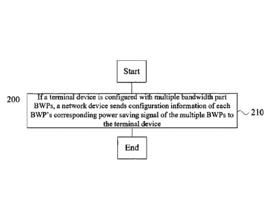
[0049] FIG. 2 is a schematic flowchart of a signal transmission method 200
according to
an embodiment of the present application. As shown in FIG. 2, the method 200
includes part
or all of the following:
[0050] S210, if a terminal device is configured with multiple Bandwidth
Parts (BWPs),
a network device sends configuration information of each BWP's corresponding
power
saving signal of the multiple BWPs to the terminal device.
[0051] When the terminal device is configured with the multiple BWPs,
configuration
of the power saving signal by a network may be per-BWP configuration, that is,
the network
separately configures a corresponding power saving signal for each BWP. For
example,
frequency domain resource positions and/or time domain resource positions of
the power
saving signal can be configured, or the number of times that the power saving
signal is sent
can also be configured, or a numerology of the power saving signal can be
configured, such
as a subcarrier interval. In this way, when a certain BWP is in an activated
state, the terminal
device can acquire configuration information of its corresponding power saving
signal.
Thereby, a better power saving gain can be achieved.
9
Date Recue/Date Received 2021-01-26
CA 03107510 2021-01-25
[0052] It should be noted that the configuration information of the each
BWP's
corresponding power saving signal may also be appointed by the protocol. For
example, the
protocol may appoint multiple BWPs, and specifically may appoint bandwidth
ranges of the
multiple BWPs. The protocol may further appoint the frequency domain resource
positions
and/or the time domain resource positions of the each BWP's corresponding
power saving
signal, and which are configured inside the terminal device. The network
device can acquire
the configuration information of the each BWP's corresponding power saving
signal in
advance. When a certain BWP is in the activated state, and the network device
needs to send
the power saving signal, the network device can determine configuration
information of the
activated BWP's corresponding power saving signal, and then the network device
sends the
power saving signal according to the acquired configuration information. For
example, the
power saving signal is sent on the configuration information.
[0053] Optionally, when the network device sends the configuration
information of the
each BWP's corresponding power saving signal to the terminal device, the
configuration
information of the power saving signal may be included in configuration
information of its
corresponding BWP. That is, the network device sends configuration information
of each
BWP to the terminal device, and also configures the power saving signal of the
corresponding BWP, and carries the configuration information of the power
saving signal of
the corresponding BWP in the configuration information of the BWP. For
example, the
configuration information of the BWP may include a bandwidth range of the BWP,
a
numerology, and measurement-related parameters (radio resource management
(RRM)
measurement or radio link monitoring (RLM) measurement), and the like. The
configuration
information of the BWP may also include time-frequency resource positions of
the
corresponding power saving signal and the like. Therefore, the network device
can
accomplish both configuration of the BWP and configuration of the
corresponding power
saving signal through a single signaling, which saves signaling overhead.
[0054] Optionally, frequency domain resources of the each BWP's
corresponding power
saving signal are located inside a bandwidth range of its corresponding BWP,
or, frequency
Date Recue/Date Received 2021-01-26
CA 03107510 2021-01-25
domain resources of the each BWP's corresponding power saving signal are
located outside
the bandwidth range of its corresponding BWP, or, the multiple BWPs are
divided into a first
BWP set and a second BWP set, and frequency domain resources of each BWP's
corresponding power saving signal in the first BWP set are located inside a
bandwidth range
of its corresponding BWP, and frequency domain resources of the each BWP's
corresponding power saving signal in the second BWP set are located outside a
bandwidth
range of its corresponding BWP.
[0055] The first embodiment to the third embodiment of the present
application will be
described in detail below in combination with FIGS. 3 to 5.
[0056] Assuming that the network configures three BWPs to the terminal, BWP
1, BWP2,
and BWP3, respectively. The power saving signals configured by the network for
the three
BWPs are respectively shown in FIGS. 3 to 5.
[0057] In FIG. 3, the frequency domain resources of the each BWP's
corresponding
power saving signal are located inside the bandwidth range of its
corresponding BWP.
Specifically, BWP 1 's corresponding power saving signal is located in BWP 1
on frequency
domain, BWP2's corresponding power saving signal is located in BWP2 on
frequency
domain, and BWP3 's corresponding power saving signal is located in BWP3 on
frequency
domain.
[0058] That is, when a certain BWP is activated, the network device can
send a
corresponding power saving signal to the terminal device on this BWP, and the
terminal
device can receive the corresponding power saving signal sent by the network
device on this
BWP, avoiding unnecessary frequency hopping when receiving the power saving
signal.
[0059] In FIG. 4, the frequency domain resources of the each BWP's
corresponding
power saving signal are outside the bandwidth range of the corresponding BWP.
Specifically,
the BWP1's corresponding power saving signal is located in BWP3 on frequency
domain,
the BWP2's corresponding power saving signal corresponding to BWP2 is located
in BWP1
on frequency domain, and the BWP3's corresponding power saving signal is
located in
BWP2 on frequency domain.
11
Date Recue/Date Received 2021-01-26
CA 03107510 2021-01-25
[0060] In FIG. 5, among the multiple BWPs, frequency domain resources of
some BWPs'
corresponding power saving signals are located inside bandwidth ranges of
their
corresponding BWPs, and frequency domain resources of other BWPs'
corresponding power
saving signals are located outside bandwidth ranges of their corresponding
BWPs. For
example, the frequency domain resources of the multiple BWPs' corresponding
power
saving signals may be located inside a bandwidth range of the same BWP.
Specifically, the
power saving signals respectively corresponding to BWP1, BWP2, and BWP3 are
all located
in BWP1 on frequency domain. In other words, the power saving signals
respectively
corresponding to BWP2 and BWP3 are located in a BWP outside bandwidth ranges
respective occupied on frequency domains, and the power saving signal
corresponding to
BWP1 is located inside a bandwidth range of itself on frequency domains.
[0061] The frequency domain resources of the multiple BWPs' corresponding
power
saving signals may also be located inside bandwidth ranges of some BWPs. For
example, if
the terminal is configured with 4 BWPs, BWP1, BWP2, BWP3, and BWP4, the
frequency
domain resources of the each BWP's corresponding power saving signal may be
located
inside bandwidth ranges of BWP1 and BWP2, for example, the frequency domain
resources
of the power saving signals corresponding to BWP1 - BWP4 are all located in
BWP1 and
BWP2. FIG. 5 is only for illustration and is not intended to be limiting.
[0062] Optionally, when the frequency domain resources of the power saving
signals
respectively corresponding to the multiple BWPs configured to the terminal
device are
located inside the bandwidth range of the same BWP, the BWP may be a default
BWP or an
initial active downlink BWP.
[0063] Optionally, the following attributes of the power saving signals
respectively
corresponding to the multiple BWPs may be all the same or different, or may be
partly the
same, and other parts may be different. This attribute can be a bandwidth of
the power saving
signal, that is, the frequency domain width of the power saving signal. For
example, some
BWPs' corresponding power saving signals can use a relatively large signal
bandwidth, and
some BWPs' corresponding power saving signals can use a smaller signal
bandwidth. This
12
Date Recue/Date Received 2021-01-26
CA 03107510 2021-01-25
attribute can also be a sequence type used by the power saving signal. For
example, some
BWPs' corresponding power saving signals can use Zadoff Chu (ZC) sequence, and
some
BWPs' corresponding power saving signals can use pseudo-random sequence. This
attribute
can also be a sequence number of the power saving signal. For example,
assuming that the
power saving signal uses the ZC sequence, different BWPs can use different ZC
sequence
cyclic shifts, and different ZC sequence cyclic shifts can correspond to
different sequence
numbers, that is, having different sequence numbers.
[0064] It should be understood that the power saving signal in the
embodiments of the
present application is essentially an indication signal, which may be the
aforementioned
WUS, or may be some other signals, for example, it may reuse existing
synchronization
signal/physical broadcast channel (SS/PBCH) blocks, a PDCCH channel itself, or
a channel
or signal of a candidate resource that occupies the PDCCH, that is, as long as
the terminal
device receives or does not receive these SS/PBCH blocks or the PDCCH channel
itself or
the channel or signal of the candidate resource that occupies the PDCCH, it
can be
determined that detection of the PDCCH in a corresponding receiving window is
not
performed. The network device and the terminal device can agree on these rules
in advance.
The embodiments of the present application does not limit the specific
expression manner of
the power saving signal.
[0065] For example, for the terminal in an idle state, the power saving
signal may be a
wake up signal, the wake up signal is used to wake up the terminal, and a
timing relationship
between the wake up signal and the PO may be configured by the network device.
[0066] After the network device sends the configuration information of the
multiple
BWPs' corresponding power saving signals to the terminal device, when the
power saving
signal needs to be sent, configuration information of a currently activated
BWP's
corresponding power saving signal can first be acquired, and then the
currently activated
BWP's corresponding power saving signal can be sent to the terminal device
according to
the configuration information.
13
Date Recue/Date Received 2021-01-26
CA 03107510 2021-01-25
[0067] For the network device, a power saving signal sent on a time-
frequency resource
of one power saving signal may be directed to at least one sending window on
the currently
activated BWP, and the sending window may be a sending window of DRX, that is,
the
above-mentioned "On Duration", the sending window may also be a Paging
Occasion (PO),
or a monitoring window of the PDCCH, that is, a PDCCH search space, and the
like. For the
terminal device, a power saving signal received on the time-frequency resource
of one power
saving signal may be directed to at least one receiving window on a currently
activated BWP,
and the receiving window may be a sending window of DRX, a Paging Occasion, or
a
PDCCH search space, and the like. Once the terminal device receives the power
saving
signal, it can perform detection of the PDCCH in a corresponding receiving
window. If not
received, the terminal device does not perform the detection of the PDCCH in
the
corresponding receiving window.
[0068] It should be understood that the power saving signal may also be
used to indicate
to the terminal device that detection of the PDCCH is not performed in a
corresponding
receiving window. That is, once the terminal device receives the power saying
signal, it does
not perfolin the detection of the PDCCH in the corresponding receiving window.
If not
received, the terminal device performs the detection of the PDCCH in the
corresponding
receiving window.
[0069] The sending window or receiving window corresponding to a power
saving signal
involved here may be a first sending window or a first receiving window after
the power
saving signal, or other subsequent sending window or receiving window, or may
be
subsequent multiple sending windows or receiving windows, the embodiments of
the present
application does not limit thereto.
[0070] After the BWP switching, the network device sends the power saving
signal to
the terminal device on a configuration resource of the power saving signal
corresponding to
the BWP after the switching. Similarly, the terminal device receives the power
saving signal
on the configuration resource of the power saving signal corresponding to the
BWP after the
switching.
14
Date Recue/Date Received 2021-01-26
CA 03107510 2021-01-25
[0071] FIG. 6 is a schematic block diagram of a signal transmission method
300
according to an embodiment of the present application. As shown in FIG. 6, the
method 300
includes some or all of the following:
[0072] S310, if a terminal device is configured with multiple Bandwidth
Parts (BWPs),
the terminal device receives configuration information of each BWP's
corresponding power
saving signal of the multiple BWPs sent by a network device.
[0073] Therefore, the signal transmission method of the embodiment of the
present
application, by individually configuring power saving signals for the multiple
BWPs, it is
beneficial to improve the flexibility of the terminal device to receive the
power saving signals,
thereby a better power saving gain can be achieved.
[0074] Optionally, in the embodiment of the present application, the
configuration
information of the each BWP's corresponding power saving signal is carried in
configuration
information of its corresponding BWP.
[0075] Optionally, in the embodiment of the present application, frequency
domain
resources of the each BWP's corresponding power saying signal are located
inside a
bandwidth range of its corresponding BWP, or, frequency domain resources of
the each
BWP's corresponding power saving signal are located outside the bandwidth
range of its
corresponding BWP.
[0076] Optionally, in the embodiment of the present application, the
multiple BWPs are
divided into a first BWP set and a second BWP set, and frequency domain
resources of each
BWP's corresponding power saving signal in the first BWP set are located
inside a
bandwidth range of its corresponding BWP, and frequency domain resources of
each BWP's
corresponding power saying signal in the second BWP set are located outside
the bandwidth
range of its corresponding BWP.
[0077] Optionally, in the embodiment of the present application, the first
BWP set
includes a first BWP, and the frequency domain resources of the each BWP's
corresponding
power saving signal in the second BWP set are located inside a bandwidth range
of the first
BWP.
Date Recue/Date Received 2021-01-26
CA 03107510 2021-01-25
[0078] Optionally, in the embodiment of the present application, the first
BWP is a
default BWP or an initial active downlink BWP of the terminal device.
[0079] Optionally, in the embodiment of the present application, at least
two BWPs'
respective power saving signals of the multiple BWPs are different in terms of
at least one
attribute of the following attributes: bandwidth of the power saving signal,
sequence type
used by the power saving signal, and sequence number of the power saving
signal.
[0080] Optionally, in the embodiment of the present application, the method
further
includes: receiving, by the terminal device if a second BWP of the multiple
BWPs is in an
activated state, the second BWP's corresponding power saving signal sent by
the network
device according to configuration information of the second BWP's
corresponding power
saving signal.
[0081] Optionally, in the embodiment of the present application, the method
further
includes: determining, by the terminal device, that Physical Downlink Control
Channel
(PDCCH) detection is performed in at least one window on the second BWP
according to
the second BWP's corresponding power saving signal, or determining, by the
terminal
device, that Physical Downlink Control Channel (PDCCH) detection is not
performed in at
least one window on the second BWP according to the second BWP's corresponding
power
saving signal.
[0082] Optionally, in the embodiment of the present application, the at
least one window
includes a Discontinuous Reception (DRX) sending window, a Paging Occasion
(PO), or a
PDCCH search space.
[0083] It should be understood that the interaction and relevant
characteristics and
functions between the terminal device and the network device described by the
terminal
device correspond to the relevant characteristics and functions of the network
device. In
other words, what message does the network device send to the terminal device,
and the
terminal device receives the corresponding message from the network device.
[0084] It should also be understood that, in various embodiments of the
present
application, the order of the sequence numbers of the above processes does not
mean an
16
Date Recue/Date Received 2021-01-26
CA 03107510 2021-01-25
order of an execution sequence, and the execution sequence of each process
should be
determined by its function and internal logic, and should not constitute any
limitation to the
implementation of the embodiments of the present application.
[0085] The methods for transmitting signals according to the embodiments of
the present
application have been described in detail above. An apparatus for transmitting
signals
according to the embodiments of the present application will be described
below in
combination with FIGS. 7 to 10. The technical features described in the method
embodiments are applicable to the following apparatus embodiments.
[0086] FIG. 7 shows a schematic block diagram of a network device 400
according to
an embodiment of the present application. As shown in FIG. 7, the network
device 400
includes:
[0087] a transceiver unit 410, is configured to send, if a terminal device
is configured
with multiple Bandwidth Parts (BWPs), configuration information of each BWP's
corresponding power saving signal of the multiple BWPs to the terminal device.
[0088] Optionally, in the embodiment of the present application, the
configuration
information of the each BWP's corresponding power saving signal is carried in
configuration
information of its corresponding BWP.
[0089] Optionally, in the embodiment of the present application, frequency
domain
resources of the each BWP's corresponding power saving signal are located
inside a
bandwidth range of its corresponding BWP, or, frequency domain resources of
the each
BWP's corresponding power saving signal are located outside the bandwidth
range of its
corresponding BWP.
[0090] Optionally, in the embodiment of the present application, the
multiple BWPs are
divided into a first BWP set and a second BWP set, and frequency domain
resources of each
BWP's corresponding power saving signal in the first BWP set are located
inside a
bandwidth range of its corresponding BWP, and frequency domain resources of
each BWP's
corresponding power saving signal in the second BWP set are located outside
the bandwidth
range of its corresponding BWP.
17
Date Recue/Date Received 2021-01-26
CA 03107510 2021-01-25
[0091] Optionally, in the embodiment of the present application, the first
BWP set
includes a first BWP, and the frequency domain resources of the each BWP's
corresponding
power saving signal in the second BWP set are located inside a bandwidth range
of the first
BWP.
[0092] Optionally, in the embodiment of the present application, the first
BWP is a
default BWP or an initial active downlink BWP of the terminal device.
[0093] Optionally, in the embodiment of the present application, at least
two BWPs'
respective power saving signals of the multiple BWPs are different in terms of
at least one
attribute of the following attributes: bandwidth of the power saving signal,
sequence type
used by the power saving signal, and sequence number of the power saving
signal.
[0094] Optionally, in the embodiment of the present application, the
transceiver unit is
further configured to: send, if a second BWP of the multiple BWPs is in an
activated state,
the second BWP's corresponding power saving signal to the terminal device
according to
the configuration information of the second BWP's corresponding power saving
signal.
[0095] Optionally, in the embodiment of the present application, the second
BWP's
corresponding power saving signal corresponds to at least one window on the
second BWP,
and the at least one window comprises a Discontinuous Reception (DRX) sending
window,
a Paging Occasion (PO) or a Physical Downlink Control Channel (PDCCH) search
space.
[0096] It should be understood that the network device 400 according to the
embodiment
of the present application may correspond to the network device in the method
embodiments
of the present application, and the above and other operations and/or
functions of each unit
in the network device 400 are respectively to implement the corresponding
processes of the
network device in the method in FIG. 2. For brevity, details are not described
here again.
[0097] FIG. 8 shows a schematic block diagram of a terminal device 500
according to
an embodiment of the present application. As shown in FIG. 8, the terminal
device 500
includes:
18
Date Recue/Date Received 2021-01-26
CA 03107510 2021-01-25
[0098] a transceiver unit 510, is configured to receive, if the terminal
device is
configured with multiple Bandwidth Parts (BWPs), configuration information of
each
BWP's corresponding power saving signal of the multiple BWPs sent by a network
device.
[0099] Optionally, in the embodiment of the present application, the
configuration
information of the each BWP's corresponding power saving signal is carried in
configuration
information of its corresponding BWP.
[0100] Optionally, in the embodiment of the present application, frequency
domain
resources of the each BWP's corresponding power saving signal are located
inside a
bandwidth range of its corresponding BWP, or, frequency domain resources of
the each
BWP's corresponding power saving signal are located outside the bandwidth
range of its
corresponding BWP.
[0101] Optionally, in the embodiment of the present application, the
multiple BWPs are
divided into a first BWP set and a second BWP set, and frequency domain
resources of each
BWP's corresponding power saving signal in the first BWP set are located
inside a
bandwidth range of its corresponding BWP, and frequency domain resources of
each BWP 's
corresponding power saving signal in the second BWP set are located outside a
bandwidth
range of its corresponding BWP.
[0102] Optionally, in the embodiment of the present application, the first
BWP set
includes a first BWP, and the frequency domain resources of the each BWP's
corresponding
power saving signal in the second BWP set are located inside a bandwidth range
of the first
BWP.
[0103] Optionally, in the embodiment of the present application, the first
BWP is a
default BWP or an initial active downlink BWP of the terminal device.
[0104] Optionally, in the embodiment of the present application, at least
two BWPs'
respective power saving signals of the multiple BWPs are different in terms of
at least one
attribute of the following attributes: bandwidth of the power saving signal,
sequence type
used by the power saving signal, and sequence number of the power saving
signal.
19
Date Recue/Date Received 2021-01-26
CA 03107510 2021-01-25
[0105] Optionally, in the embodiment of the present application, the
transceiver unit is
further configured to: receive, if a second BWP of the multiple BWPs is in an
activated state,
the second BWP's corresponding power saving signal sent by the network device
according
to the configuration information of the second BWP's corresponding power
saving signal.
[0106] Optionally, in the embodiment of the present application, the
terminal device
further includes: a processing unit, configured to determine that Physical
Downlink Control
Channel (PDCCH) detection is performed in at least one window on the second
BWP
according to the second BWP's corresponding power saving signal, or determine
that
Physical Downlink Control Channel (PDCCH) detection is not performed in at
least one
window on the second BWP according to the second BWP's corresponding power
saving
signal.
[0107] Optionally, in the embodiment of the present application, the at
least one window
includes a Discontinuous Reception (DRX) sending window, a Paging Occasion
(PO), or a
PDCCH search space.
[0108] It should be understood that the terminal device 500 according to
the embodiment
of the present application may correspond to the terminal device in the method
embodiments
of the present application, and the above and other operations and/or
functions of each unit
in the terminal device 500 are respectively to implement the corresponding
processes of the
terminal device in the method in FIG. 6. For brevity, details are not
described here again.
[0109] As shown in FIG. 9, an embodiment of the present application further
provides a
network device 600. The network device 600 may be the network device 400 in
FIG. 7,
which can be used to perform content of the network device corresponding to
the method
200 in FIG. 2. The network device 600 shown in FIG. 9 includes a processor
610, and the
processor 610 can invoke and run a computer program from a memory to implement
the
methods in the embodiments of the present application.
[0110] Optionally, as shown in FIG. 9, the network device 600 may further
include a
memory 620. The processor 610 may invoke and run a computer program from the
memory
620 to implement the methods in the embodiments of the present application.
Date Recue/Date Received 2021-01-26
CA 03107510 2021-01-25
101 1 1] The memory 620 may be a separate device independent of the
processor 610, or
may be integrated in the processor 610.
[0112] Optionally, as shown in FIG. 9, the network device 600 may further
include a
transceiver 630, and the processor 610 may control the transceiver 630 to
communicate with
other devices, and specifically, may send information or data to other
devices, or receive
information or data sent by other devices.
[0113] The transceiver 630 may include a transmitter and a receiver. The
transceiver 630
may further include antennas, and the number of the antennas may be one or
more.
[0114] Optionally, the network device 600 may be the network device in the
embodiments of the present application, and the network device 600 may
implement the
corresponding processes implemented by the network device in various methods
in the
embodiments of the present application. For brevity, details are not described
herein again.
[0115] In a specific implementation, the transceiver unit in the network
device 400 may
be implemented by the transceiver 630 in FIG. 9.
[0116] As shown in FIG. 10, an embodiment of the present application
further provides
a terminal device 700. The terminal device 700 may be the terminal device 500
in FIG. 8
and can be used to perform content of the terminal device corresponding to the
method 300
in FIG. 6. The terminal device 700 shown in FIG. 10 includes a processor 710.
The processor
710 can invoke and run a computer program from a memory to implement the
methods in
the embodiments of the present application.
[0117] Optionally, as shown in FIG. 10, the terminal device 700 may further
include a
memory 720. The processor 710 may invoke and run a computer program from the
memory
720 to implement the methods in the embodiments of the present application.
[0118] The memory 720 may be a separate device independent of the processor
710, or
may be integrated in the processor 710.
[0119] Optionally, as shown in FIG. 10, the terminal device 700 may further
include a
transceiver 730, and the processor 710 may control the transceiver 730 to
communicate with
21
Date Recue/Date Received 2021-01-26
CA 03107510 2021-01-25
other devices, and specifically, may send information or data to other
devices, or receive
information or data sent by other devices.
[0120] The transceiver 730 may include a transmitter and a receiver. The
transceiver 730
may further include antennas, and the number of the antennas may be one or
more.
[0121] Optionally, the terminal device 700 may be the terminal device in
the
embodiments of the present application, and the terminal device 700 may
implement the
corresponding processes implemented by the terminal device in various methods
in the
embodiments of the present application. For brevity, details are not described
herein again.
[0122] In a specific implementation, the processing unit in the terminal
device 500 may
be implemented by the processor 710 in FIG. 10. The transceiver unit 510 in
the terminal
device 500 may be implemented by the transceiver 730 in FIG. 10.
[0123] FIG. 11 is a schematic structural diagram of a chip according to an
embodiment
of the present application. The chip 800 shown in FIG. 11 includes a processor
810, and the
processor 810 can invoke and run a computer program from a memory to implement
the
methods in the embodiments of the present application.
[0124] Optionally, as shown in FIG. 11, the chip 800 may further include a
memory 820.
The processor 810 may invoke and run a computer program from the memory 820 to
implement the methods in the embodiments of the present application.
[0125] The memory 820 may be a separate device independent of the processor
810, or
may be integrated in the processor 810.
[0126] Optionally, the chip 800 may further include an input interface 830.
The processor
810 may control the input interface 830 to communicate with other devices or
chips,
specifically, information or data sent by other devices or chips may be
acquired.
[0127] Optionally, the chip 800 may further include an output interface
840. The
processor 810 may control the output interface 840 to communicate with other
devices or
chips, specifically, information or data to other devices or chips may be
output.
[0128] Optionally, the chip may be applied to the network device in the
embodiments of
the present application, and the chip may implement the corresponding
processes
22
Date Recue/Date Received 2021-01-26
CA 03107510 2021-01-25
implemented by the network device in various methods in the embodiments of the
present
application. For brevity, details are not described herein.
[0129] Optionally, the chip may be applied to the terminal device in the
embodiments of
the present application, and the chip may implement the corresponding
processes
implemented by the terminal device in various methods in the embodiments of
the present
application. For brevity, details are not described herein again.
[0130] It should be understood that the chip mentioned in the embodiments
of the present
application may also be referred as a system-level chip, a system chip, a chip
system or a
system-on-chip.
[0131] FIG. 12 is a schematic block diagram of a communication system 900
according
to an embodiment of the present application. As shown in FIG. 12, the
communication
system 900 includes a terminal device 910 and a network device 920.
[0132] The terminal device 910 may be used to implement the corresponding
functions
implemented by the terminal device in the foregoing methods, and the network
device 920
may be used to implement the corresponding functions implemented by the
network device
in the foregoing methods. For brevity, details are not described herein again.
[0133] It should be understood that the processor in an embodiment of the
present
application may be an integrated circuit chip with signal processing
capability. In an
implementation process, each step of the foregoing method embodiments may be
completed
by an integrated logic circuit of hardware in a processor or instructions in a
form of software.
The above processor may be a general-purpose processor, a digital signal
processor (DSP),
an application specific integrated circuit (ASIC), a field programmable gate
array (FPGA),
or other programming logic devices, discrete gates or transistor logic
devices, discrete
hardware components. Various methods, steps, and logical block diagrams
disclosed in the
embodiments of the present application may be implemented or executed. A
general-purpose
processor may be a microprocessor or the processor may be any conventional
processor or
the like. The steps in combination with the methods disclosed in the
embodiments of the
present application may be directly embodied by a hardware decoding processor,
or may be
23
Date Recue/Date Received 2021-01-26
CA 03107510 2021-01-25
performed by a combination of hardware and software modules in the decoding
processor.
The software module can be located in a conventional storage medium in the art
such as
random access memory, flash memory, read-only memory, programmable read-only
memory,
or electrically erasable programmable memory, register, or the like. The
storage medium is
located in the memory, and the processor reads information in the memory and
combines its
hardware to complete the steps of the above methods.
[0134] It can be understood that the memory in the embodiments of the
present
application may be a volatile memory or a non-volatile memory, or may include
both volatile
and non-volatile memory. Where, the non-volatile memory may be a read-only
memory
(ROM), a programmable ROM (PROM), an erasable PROM (EPROM), an electrically
EPROM (EEPROM) or flash memory. The volatile memory may be a random access
memory (RAM), which is used as an external cache. By way of example but not
limitation,
many forms of RAM are available, such as static RAM (SRAM), dynamic RAM
(DRAM),
synchronous DRAM (SDRAM), double data rate SDRAM (DDR SDRAM), enhanced
SDRAM (ESDRAM), synchlink DRAM (SLDRAM ) and direct rambus RAM (DR RAM).
It should be noted that the memory of the systems and methods described herein
is intended
to include, but is not limited to, these and any other suitable types of
memory.
[0135] It should be understood that the foregoing memory is exemplary but
not
limitation. For example, the memory in the embodiments of the present
application may also
be static RAM (SRAM), dynamic RAM (DRAM), synchronous DRAM (SDRAM), double
data rate SDRAM (DDR SDRAM), enhanced SDRAM (ESDRAM), synch link DRAM
(SLDRAM) and direct rambus RAM (DR RAM), or the like. That is, the memories in
the
embodiments of the present application are intended to include, but not
limited to, these and
any other suitable types of memories.
[0136] An embodiment of the present application further provides a computer-
readable
storage medium for storing computer programs.
[0137] Optionally, the computer-readable storage medium can be applied to
the network
device in the embodiments of the present application, and the computer
programs cause a
24
Date Recue/Date Received 2021-01-26
CA 03107510 2021-01-25
computer to execute the corresponding process implemented by the network
device in
various methods in the embodiments of the present application. For brevity,
details are not
described herein again.
[0138] Optionally, the computer-readable storage medium can be applied to
the terminal
device in the embodiments of the present application, and the computer
programs cause a
computer to execute the corresponding process implemented by the mobile
terminal/terminal
device in various methods in the embodiments of the present application. For
brevity, details
are not described herein again.
[0139] An embodiment of the present application further provides a computer
program
product, including computer program instructions.
[0140] Optionally, the computer program product can be applied to the
network device
in the embodiments of the present application, and the computer program
instructions cause
a computer to execute the corresponding process implemented by the network
device in
various methods in the embodiments of the present application. For brevity,
details are not
described herein again.
[0141] Optionally, the computer program product can be applied to the
terminal device
in the embodiments of the present application, and the computer program
instructions cause
a computer to execute the corresponding process implemented by the mobile
terminal/terminal device in various methods in the embodiments of the present
application.
For brevity, details are not described herein again.
[0142] An embodiment of the present application also provides a computer
program.
[0143] Optionally, the computer program may be applied to the network
device in the
embodiments of the present application. When the computer program is run on a
computer,
the computer is caused to execute the corresponding process implemented by the
network
device in various methods in the embodiments of the present application. For
brevity, details
are not described herein again.
[0144] Optionally, the computer program may be applied to the terminal
device in the
embodiments of the present application. When the computer program is run on a
computer,
Date Recue/Date Received 2021-01-26
CA 03107510 2021-01-25
the computer is caused to execute the corresponding process implemented by the
terminal
device in various methods in the embodiments of the present application. For
brevity, details
are not described herein again.
[0145] Those of ordinary skill in the art may appreciate that the units and
algorithm steps
of the various examples described in combination with the embodiments
disclosed herein
can be implemented by electronic hardware, or a combination of computer
software and
electronic hardware. Whether these functions are performed in hardware or
software depends
on specific applications and design constraints of the technical solutions. A
person skilled in
the art can use different methods to implement the described functions for
each specific
application, but such implementation should not be considered to be beyond the
scope of the
present application.
[0146] A person skilled in the art can clearly understand that, for the
convenience and
brevity of description, the specific operation processes of the systems,
devices, and units
described above can refer to the corresponding processes in the foregoing
method
embodiments, details are not described herein again.
[0147] In the several embodiments provided in the present application, it
should be
understood that the disclosed systems, devices, and methods may be implemented
in other
ways. For example, the device embodiments described above are merely
illustrative. For
example, the division of the unit is only a logical function division. In an
actual
implementation, there may be another division manner. For example, multiple
units or
components may be combined or may be integrated into another system, or some
features
can be ignored or not executed. In addition, the shown or discussed coupling
or direct
coupling or communication connection between each other may be an indirect
coupling or
communication connection through some interfaces, devices or units, and may be
in
electrical, mechanical or other forms.
[0148] The units described as separate components may or may not be
physically
separated, and the components displayed as units may or may not be physical
units, that is,
may be located in one place, or may be distributed to multiple network units.
Some or all of
26
Date Recue/Date Received 2021-01-26
CA 03107510 2021-01-25
the units may be selected according to actual needs to implement the purpose
of the solution
of the present embodiment.
[0149] In addition, each functional unit in each embodiment of the present
application
may be integrated into one processing unit, or each unit may exist physically
separately, or
two or more units may be integrated into one unit.
[0150] This functionality, if implemented as a software functional unit and
sold or used
as a standalone product, can be stored in a computer readable storage medium.
Based on
such understanding, the technical solution of the present application
essentially, or a part of
contributing to the prior art, or a part of the technical solution, may be
embodied in a form
of a software product, the computer software product is stored in a storage
medium, which
includes a number of instructions for causing a computer device (which may be
a personal
computer, server, or network device, or the like) to perform all or part of
the steps of various
embodiments of the present application. The foregoing storage medium includes
various
medium that can store program codes: a U disk, a mobile hard disk, a read-only
memory
(ROM), a random access memory (RAM), a magnetic disk, or an optical disk, or
the like.
The above mentioned are only specific implementations of the present
application, but the
protection scope of the present application is not limited thereto. Any person
skilled in the
art can easily think of changes or substitutions within the technical scope
disclosed in the
present application, which should be covered in the protection scope of the
present
application. Therefore, the protection scope of the present application should
be determined
by the protection scope of the claims.
27
Date Recue/Date Received 2021-01-26