Note: Descriptions are shown in the official language in which they were submitted.
CA 03107955 2021-01-28
WO 2019/023794
PCT/CA2018/050929
Optical Sensing Methods and Systems for Transformers, and the Construction
Thereof
Field
[1] The described embodiments relate to sensing methods, and systems
thereof,
for transformers, and the construction thereof. In particular, at least some
of the
described methods and systems are directed to sensing the operating conditions
within a transformer.
Background
[2] Faults within a transformer system, such as a power system or reactor
system, can be difficult to detect in a timely manner. Faults at a transformer
can be
caused by physical breakdowns, design flaws, and electrical and/or magnetic
flux
fluctuations resulting from temperature variation (e.g., hot spots) and/or
physical
stress. These faults can occur deep within the transformers and can occur
fairly
quickly, possibly even within minutes. These faults can cause significant
failures
within the transformer system and can even cause the system to explode.
[3] Point sensors can be embedded within the transformer system for
detecting
operating condition(s) at a specific location. To capture sufficient data to
represent
the operating condition of the overall system, a significant number of point
sensors
are required to be installed throughout the system. A detection range of the
point
sensors can be limited and so, point sensors may not detect nearby faults if
they
occur outside the spatial detection range.
Summary
[4] The various embodiments described herein generally relate to sensing
-- methods, systems and the construction thereof.
[5] In accordance with some embodiments, a transformer system includes: a
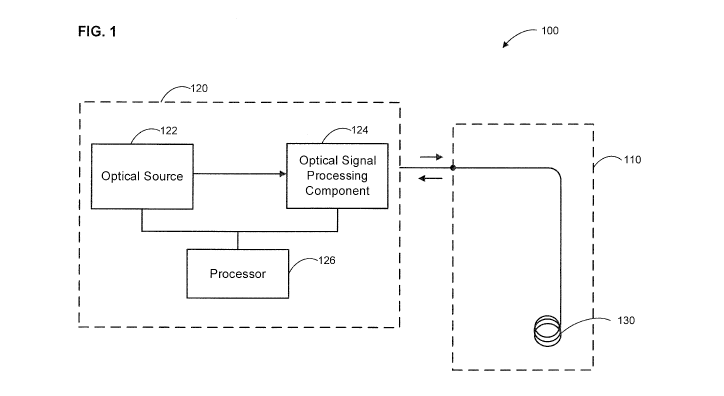
core having: a bottom plate; two or more limbs mounted to the bottom plate;
and a
top plate mounted to the two or more limbs to enclose the core, wherein at
least one
of the bottom plate, the top plate and a limb is formed with a sensing
component
therein; and a winding assembly wound around each respective limb.
[6] In some embodiments, the at least one of the bottom plate, the top
plate and
the limb includes at least one sensing layer within a stack of laminated
layers, each
¨ 1 ¨
CA 03107955 2021-01-28
WO 2019/023794
PCT/CA2018/050929
sensing layer including a spacer layer with the sensing component mounted
therein;
and an electrical coupling between laminated layers neighboring the sensing
layer.
[7] In some embodiments, the at least one sensing layer includes a sensing
layer, and the sensing layer is positioned at a substantially central position
within the
stack of laminated layers.
[8] In some embodiments, the at least one sensing layer includes two or
more
sensing layers, and the two or more sensing layers are distributed
substantially
equidistant from each other within the stack of laminated layers.
[9] In some embodiments, each sensing layer includes: the spacer layer with
a
path defined therein; and the sensing component mounted within the path.
[10] In some embodiments, the path extends along a length and/or a width of
the
spacer layer.
[11] In some embodiments, at least a portion of the path includes an
oscillating
pattern.
[12] In some embodiments, the sensing component includes an optical fiber.
[13] In accordance with some embodiments, a method of constructing a core for
a
transformer system includes: forming a core sensing element by: mounting a
sensing component to a spacer layer to form a sensing layer; compressing the
sensing layer within a stack of laminated layers; and providing an electrical
coupling
between laminated layers neighboring the sensing layer; and assembling the
core
using at least one core sensing element.
[14] In some embodiments, mounting the sensing component to the spacer layer
includes: defining a path within the spacer layer; and mounting the sensing
component within the path.
[15] In some embodiments, defining the path into the spacer layer includes
cutting
the path into the spacer layer. Methods for cutting the path can include
waterjet or
other methods, such as laser or with a Computer Numerical Control (CNC)
router.
[16] In some embodiments, the method further includes defining the path
lengthwise along the spacer layer.
[17] In some embodiments, the method further includes defining a portion of
the
path to have an oscillating pattern.
[18] In some embodiments, the sensing component includes an optical fiber.
¨2¨
CA 03107955 2021-01-28
WO 2019/023794
PCT/CA2018/050929
[19] In some embodiments, mounting the sensing component within the path
includes: adhering the optical fiber within the path.
[20] In some embodiments, providing the electrical coupling between the
laminated layers neighboring the sensing layer includes connecting the
neighboring
laminated layers with a bridge component.
[21] In some embodiments, forming the core sensing element includes: forming
two or more sensing layers; and providing the two or more sensing layers
within the
stack of laminated layers, wherein each sensing layer is compressed between
two
neighboring laminated layers.
[22] In some embodiments, the sensing layer is positioned at a substantially
central position within the stack of laminated layers.
[23] In some embodiments, the core includes a bottom plate, two or more limbs
mounted to the bottom plate, and a top plate mounted to the two or more limbs
to
enclose the core; and at least one of the bottom plate, a limb and the top
plate
includes the core sensing element.
[24] In accordance with some embodiments, a method for detecting operating
conditions within a transformer includes: mounting a sensing component within
a
core of the transformer; receiving an input optical signal from an optical
source;
transmitting a version of the input optical signal to the sensing component,
wherein
the input optical signal is defined with a carrier frequency at a Brillouin
value
characterized for the sensing component; receiving a plurality of reflected
optical
data signals from the sensing component in response to an interaction between
the
sensing component and the input optical signal; and analyzing the plurality of
reflected optical data signals to detect one or more operating conditions
within the
transformer.
[25] In some embodiments, applying the input optical signal at the Brillouin
frequency further includes applying a Brillouin Optical Time Doman Analysis
(BOTDA).
[26] In some embodiments, the sensing component includes an optical fiber; and
the method includes: forming a core sensing element by: mounting the sensing
component to a spacer layer to form a sensing layer; compressing the sensing
layer
within a stack of laminated layers; and providing an electrical coupling
between
laminated layers neighboring the sensing layer; assembling the core using at
least a
¨3¨
CA 03107955 2021-01-28
WO 2019/023794
PCT/CA2018/050929
core sensing element. The core sensing element can include multiple elements,
in
some embodiments.
[27] In some embodiments, the method includes: organizing the sensing
component into a plurality of zones; and analyzing the plurality of reflected
optical
.. data signals to detect the one or more operating conditions within the
transformer
includes: receiving a selection of one or more zones from the plurality of
zones;
identifying a set of reflected optical data signals from the plurality of the
reflected
optical data signals received from the one or more zones within the sensing
component; and conducting an analysis of the selected set of reflected optical
data
signals to determine the one or more operating conditions at the one or more
zones.
[28] In some embodiments, analyzing the plurality of reflected optical data
signals
to detect the one or more operating conditions within the transformer
includes:
detecting a variation in at least one of the one or more operating conditions
within
the transformer.
[29] In accordance with some embodiments, a system for detecting operating
conditions within a transformer includes: a sensing component mounted within a
core of the transformer; an optical signal processing component for: receiving
an
input optical signal from an optical source; transmitting a version of the
input optical
signal to the sensing component, wherein the version of the input optical
signal is
defined with a carrier frequency at a Brillouin value characterized for the
sensing
component; and receiving a plurality of reflected optical data signals from
the
sensing component in response to an interaction between the sensing component
and the version of the input optical signal; and a processor for analyzing the
plurality
of reflected optical data signals to detect one or more operating conditions
within the
transformer.
[30] In some embodiments, the optical signal processing component applies
Brillouin Optical Time Doman Analysis (BOTDA).
[31] In some embodiments, the sensing component includes an optical fiber; and
the core has: a bottom plate; two or more limbs mounted to the bottom plate;
and a
top plate mounted to the two or more limbs to enclose the core, wherein at
least one
of the bottom plate, the top plate and a limb is formed with a sensing
component
therein.
¨4¨
CA 03107955 2021-01-28
WO 2019/023794
PCT/CA2018/050929
[32] In some embodiments, the processor operates to detect a variation in at
least
one of the one or more operating conditions within the transformer.
[33] In accordance with some embodiments, a method of constructing a winding
assembly includes: forming a sensing coil, the sensing coil including: a lower
coil
portion with a lower groove defined therein, an upper coil portion with an
upper
groove defined therein, and a bonding layer coupling the lower coil portion
with the
upper coil portion, wherein the lower and upper grooves form a passage for
receiving a sensing component; and winding the sensing coil onto a coil
former.
[34] In some embodiments, the sensing component includes an optical fiber.
[35] In some embodiments, the coil former includes one of a former and a core
of
a transformer.
[36] In some embodiments, each of the lower groove and upper groove is formed
at a substantially central position of the respective lower and upper coil
portions.
Brief Description of the Drawings
[37] Several embodiments will now be described in detail with reference to the
drawings, in which:
FIG. 1 is a block diagram of an optical sensing system in accordance with an
example embodiment;
FIG. 2A is a block diagram of a control system in accordance with an example
embodiment;
FIG. 2B is a block diagram of a control system in accordance with another
example embodiment;
FIG. 3A is a graph showing a waveform generated by the control system in
accordance with an example embodiment;
FIG. 3B is a screenshot of a waveform generated by the control system in
accordance with another example embodiment;
FIG. 4 is a partial perspective view of a partially constructed winding
assembly in accordance with an example embodiment;
FIG. 5A is a perspective view of a partially constructed winding assembly in
accordance with an example embodiment;
FIG. 5B is a top cross-sectional view of the partially constructed winding
assembly shown in FIG. 5A,
¨5¨
CA 03107955 2021-01-28
WO 2019/023794
PCT/CA2018/050929
FIG. 6 is a side view of a winding assembly in accordance with another
example embodiment;
FIG. 7 is a top cross-sectional view of a winding assembly in accordance with
another example embodiment;
FIG. 8A is a partial perspective view of a partially constructed winding
assembly in accordance with another example embodiment;
FIG. 8B is a partial perspective view of the partially constructed winding
assembly shown in FIG. 8A at a later stage of construction and with a portion
of a
coil cut out;
FIG. 80 is a partial perspective view taken from the bottom of the partially
constructed winding assembly shown in FIG. 813,
FIG. 9A is a partial perspective view of a partially constructed winding
assembly in accordance with another example embodiment;
FIG. 9B is a partial perspective view of the partially constructed winding
assembly shown in FIG. 9A at a later stage of construction;
FIG. 90 is a partial perspective view of the partially constructed winding
assembly shown in FIG. 9B at a later stage of construction;
FIG. 10 is a side view of a transformer assembled with two example winding
assemblies in accordance with an example embodiment;
FIG. 11 is a perspective view of an example transformer assembled with
example winding assemblies described herein;
FIG. 12A is a diagram representing a winding assembly from a top cross-
sectional view in accordance with an example embodiment;
FIG. 12B is a diagram representing a winding assembly from a top cross-
sectional view in accordance with another example embodiment;
FIG. 13A is a cross-sectional view of an example sensing coil in accordance
with an example embodiment;
FIG. 13B is a cross-sectional view of another example sensing coil in
accordance with another example embodiment;
FIG. 14A is a cross-sectional view of a transformer in accordance with
another example embodiment;
FIG. 14B is a top view of an example center limb for the transformer shown in
FIG. 14A,
¨6¨
CA 03107955 2021-01-28
WO 2019/023794
PCT/CA2018/050929
FIG. 140 is a top view of another example center limb for the transformer
shown in FIG. 14A,
FIG. 14D is a front view of a sensing layer for the center limb shown in FIG.
14B, and
FIG. 15 shows an example template of path patterns for an example
transformer.
[38] The drawings, described below, are provided for purposes of illustration,
and
not of limitation, of the aspects and features of various examples of
embodiments
described herein. For simplicity and clarity of illustration, elements shown
in the
drawings have not necessarily been drawn to scale. The dimensions of some of
the
elements may be exaggerated relative to other elements for clarity. It will be
appreciated that for simplicity and clarity of illustration, where considered
appropriate, reference numerals may be repeated among the drawings to indicate
corresponding or analogous elements or steps.
Detailed Description of Example Embodiments
[39] During operation, an internal environment of a transformer can change
quickly and faults can occur rapidly. Faults within a transformer can be
caused by
physical breakdowns, design flaws, and electrical and/or magnetic flux
fluctuations
resulting from temperature variation (e.g., hot spots) and/or physical stress.
These
faults can cause significant failures within the transformer system and can
even
cause fire and/or explosions. It is, therefore, important to detect faults
inside the
transformer within a reasonable time and with a reasonable degree of accuracy
with
respect to the location of the fault. The internal environment of the
transformer can
also be harsh due to the exposure to corrosive chemicals. The sensing systems
described herein can facilitate the detection of these faults.
[40] The transformers described herein include any high voltage devices formed
of
a core and windings. Example transformer systems can include power systems in
which the transformer operate to convert voltage and reactor systems in which
the
transformer operates to absorb a portion of the reactive power.
[41] Reference is made to FIG. 1, which illustrates a block diagram of an
optical
sensing system 100.
¨7¨
CA 03107955 2021-01-28
WO 2019/023794
PCT/CA2018/050929
[42] The optical sensing system 100 includes a control system 120 and a
sensing
component 110. The sensing component 110 can include an optical fiber 130. The
optical fiber 130 may be coupled with a reflector at an end away from the
control
system 120.
[43] The control system 120 can apply Brillouin Optical Time-Domain Analysis
(BOTDA) for monitoring operating conditions at the sensing component 110. When
applying Brillouin Optical Time-Domain Analysis (BOTDA) to optical devices,
such
as the optical fiber 130, a shift within the Brillouin spectrum can represent
a
temperature and/or strain change at the optical fiber 130.
[44] The control system 120 includes an optical source 122, an optical signal
processing component 124 and a processor 126. As shown, the processor 126 is
in
communication with the optical source 122 and the optical signal processing
component 124.
[45] The optical source 122 can generate an input optical signal that will
travel
within the sensing component 110. For example, the optical source 122 can
include
a laser that can generate a continuous output beam, or a continuous wave. The
input optical signal generated by the optical source 122 is then directed to
the optical
signal processing component 124. Example optical sources 122 can include a
tunable laser source, and a laser diode paired with an optical filter. The
optical filter
may be tunable.
[46] As shown in FIG. 1, the optical signal processing component 124 receives
the
input optical signal from the optical source 122. The optical signal
processing
component 124 can preprocess the input optical signal before transmitting a
processed optical signal to the sensing component 110.
[47] The optical signal processing component 124 can include an optic
modulator
that can include an electro-optic modulator and/or an acousto-optic modulator
for
modulating the input optical signal. The operation of the optic modulator can
be
controlled by the processor 126. For example, the processor 126 can define a
modulation to be applied to the input optical signal and can then transmit a
corresponding modulation signal to a pulse conditioning component. The pulse
conditioning component can then generate modulation control signals for
triggering
the operation of the electro-optic modulator. In some embodiments, the pulse
¨8¨
CA 03107955 2021-01-28
WO 2019/023794
PCT/CA2018/050929
conditioning component can also include a microwave generator and a DC bias
component.
[48] The DC bias component can define certain properties of the modulated
optical signal, such as a duration of the signal. For example, the DC bias
component
can be pulsed at low frequency, such as a frequency within the kilohertz
range, to
define the duration of the spacing between the pulses to be longer than a time
of
flight within the optical fiber 130. In this way, there will be no confusion
between the
various sets of optical data signals returning from the optical fiber 130.
[49] In some embodiments, an optical filter can receive the input optical
signal
from the optical source 122 for varying the input optical signal. The optical
filter can
reduce broadband noise from the optical source 122. The optical filter can, in
some
embodiments, filter the input optical signal so that only the Brillouin
reflection
remains. For example, a Bragg filter can be included so that it passes only
the
Brillouin reflection component of the input optical signal.
[50] An optical amplifier can be included in the optical signal processing
component 124, in some embodiments, for amplifying the input optical signal,
or a
version of the input optical signal. An example optical amplifier includes an
Erbium
doped fiber amplifier.
[51] The optical signal processing component 124 can include a directional
component for directing the transmission of the input optical signal, or a
version of
the input optical signal, towards the sensing component 110. In some
embodiments,
the directional component can include an optical isolator that can prevent
unwanted
feedback. The optical isolator can be positioned before or after the optical
filter, the
electro-optic modulator, and/or the optical amplifier, in some embodiments.
[52] To facilitate the transmission of the optical signals between the
processor 126
and the sensing component 110, the optical signal processing component 124
includes a circulator for directing the processed optical signal towards the
sensing
component 110, and then directing the optical data signal received from the
sensing
component 110 towards the processor 126 for analysis.
[53] In the transmission path between the circulator and the processor 126,
various post-processing of the optical data signal may be conducted. For
example,
the optical signal processing component 124 can include an optical filter,
such as a
Bragg filter, for varying the strength of the optical data signal. Other
components,
¨9¨
CA 03107955 2021-01-28
WO 2019/023794
PCT/CA2018/050929
such as a photodetector and an amplifier, can also be included in the optical
signal
processing component 124 for processing the optical data signal before
transmitting
a processed optical data signal to the processor 126.
[54] Example implementations of the control system 120 are shown in FIGS. 2A
and 2B.
[55] As shown in FIG. 2A, an example control system 120A can include an
optical
signal processing component 124A with an optical isolator 150 and a circulator
152.
The optical isolator 150 can receive an input optical signal from the optical
source
122 and direct the input optical signal towards the circulator 152 while
preventing
unwanted feedback signals from flowing towards the optical source 122. The
circulator 152 can then direct the input optical signal towards the sensing
component
110, as well as receive optical data signals from the sensing component 110.
[56] FIG. 2B shows another example control system 120B. The control system
120B can include an optical signal processing component 124B as shown. The
optical signal processing component 124B can include an electro-optic
modulator
160 that receives an input optical signal from the optical source 122.
[57] The optical source 122 can be a continuous wave laser. The laser can be
continuously modulated at the desired frequency. The desired frequency can
vary
between and including 10GHz to 13GHz depending on the type of fiber and
coating
at the fiber. The DC bias component within the pulse conditioning component
166
can also be continuously pulsed within the kilohertz range to generate a low
frequency pulses on top of high frequency modulated signal generated by the
laser.
The modulated laser can generate the Brillouin sidebands (e.g., such as 184a,
184b
shown in FIG. 3A) and the low frequency pulses generated by the DC bias
component signal allows for the time domain analysis.
[58] The electro-optic modulator 160 can modulate the input optical signal to
square laser pulses. The square laser pulses, depending on the intended
sensing
component 110 and its environment can be within a kilohertz or hertz range.
For
conducting the Brillouin Optical Time-Domain Analysis (BOTDA), the electro-
optic
modulator 160 can generate two side bands with an equal frequency shift around
the Brillouin frequency (or the main carrier frequency) corresponding to the
sensing
component 110.
¨ 10 ¨
CA 03107955 2021-01-28
WO 2019/023794
PCT/CA2018/050929
[59] A pulse conditioning component 166 can include a microwave generator for
tuning the frequency shift of the sidebands generated by the electro-optic
modulator
160. The frequency shift of the sidebands is recorded by the processor 126.
[60] For sensing components 110 in which silica optical fibers are used, the
Brillouin frequency is approximately between 10GHz to 12GHz. FIG. 3A
illustrates
an example waveform 180 of a modulated signal generated by the electro-optic
modulator 160 for an optical fiber characterized with a Brillouin value of
approximately 12GHz. As shown in FIG. 3A, the modulated signal has three
peaks.
A main carrier peak 182 is generated by the optical source 122, side peak 184a
is
the Stokes component of the Brillouin reflection and side peak 184b is the
anti-
Stokes component.
[61] The electro-optic modulator 160 can then transmit a modulated optical
signal
towards an optical amplifier 162, which can direct a version of the modulated
optical
signal towards a circulator 164. From the circulator 164, the version of the
modulated optical signal propagates into the sensing component 110. In an
optical
fiber 130, for example, the pulses of the modulated optical signal within the
center
frequency (e.g., main carrier peak 182) interact with a back-reflected Stokes
sideband. The circulator 164 then receives a reflected data signal and directs
the
reflected data signal to a photodetector 170.
[62] As shown in FIG. 2B, a filter component 168, such as a Bragg filter, can
process the reflected data signal from the optical fiber 130 so that only the
optical
signal within the Stokes band is transmitted to the processor 126. FIG. 3B
shows a
screenshot of an example waveform 190 representing a Stokes signal 192
processed by the Bragg filter. An amplifier component 172 can be positioned
between the photodetector 170 and the processor 126.
[63] The processor 126 can then record the received Stokes band signal as a
function of its frequency shift and time, relative to each of the square laser
pulse
generated by the electro-optic modulator 160. The time associated with the
Stokes
signal can also correspond to a distance travelled along the optical fiber
130. Using
the recorded Stokes signals, the processor 126 can then spatially resolve an
operating condition of the optical fiber 130, such as temperature and/or
strain. As a
temperature of the optical fiber 130 at a particular region changes, a
resulting
Stokes signal returning from that region will vary.
¨11¨
CA 03107955 2021-01-28
WO 2019/023794
PCT/CA2018/050929
[64] By adjusting the RF modulating frequency, the level of the Brillouin
response
is varied. When the Brillouin signal is affected by external influences, such
as
temperature, the control system 120 can detect the peak Brillouin response by
sweeping the RF frequency to determine a change in temperature or strain.
[65] In some embodiments, the processor 126 can generate a set of three-
dimensional time domain waveforms with respect to time, frequency and power to
track the temperature of the various regions of the optical fiber 130 with
spatial
resolution controlled by the optical signal processing component 124 and the
processor 126. The operating conditions of the transformer in which the
optical fiber
130 is mounted can, thus, also be tracked.
[66] As will be described with reference to FIGS. 4 to 15, the sensing
component
110 can be installed within a transformer for monitoring the operating
conditions of
the transformer.
[67] During operation, the internal environment of the transformer can change
quickly and as a result, faults can occur rapidly. These faults can cause
significant
failures within the transformer system and can even cause fire and/or
explosions. It
is, therefore, important to detect faults inside the transformer within a
reasonable
time and with a reasonable degree of accuracy with respect to the location of
the
fault.
[68] By distributing the optical fiber 130 within the transformer, the
detection range
of the sensing component can be increased. The optical fiber 130 may, in some
embodiments, be wound around a coil former of the transformer more than once.
In
some embodiments, the optical fiber 130 can be positioned within a core of the
transformer. The resulting measurement data collected from each location
within the
transformer can be increased. The optical fiber 130 is also well insulated and
thus, is
protected from the corrosive environment.
[69] The construction of the optical sensing system 100 for transformers can
include mounting the sensing component 110 to a coil former of the
transformer.
The coil former can include the core or the former.
[70] In some embodiments, such as those described with reference to FIGS. 4 to
12B, a coil can be wound onto the coil former so that the sensing component
110
becomes positioned within the coil. For example, the coil former can be a
structure
on which a coil of the transformer is wound, such as a core or the former. In
some
¨ 12¨
CA 03107955 2021-01-28
WO 2019/023794
PCT/CA2018/050929
embodiments, the sensing component 110 can be embedded within the coil former.
For example, the sensing component 110 can be positioned within the core.
[71] FIG. 4 is a perspective view of an example partially constructed winding
assembly 200.
[72] The winding assembly 200 includes the core 202 around which an optical
fiber 230 and a coil 204 are wound. The optical fiber 230, in some
embodiments,
can be wound to the winding assembly 200 as multiple separate segments.
Although
multiple turns of the optical fiber 230 is shown in FIG. 4, in some
embodiments, the
optical fiber 230 can be wound a fewer number of turns around the core 202.
[73] The coil 204 is wound separately from the optical fiber 230. It is
possible that
the coil 204 is wound closer to the optical fiber 230 so that the turns in
each of the
optical fiber 230 and coil 204 are closer in proximity to each other and, in
some
embodiments, even in contact. In FIG. 4, the coil 204 and the optical fiber
230 are
alternately wound onto the core 202. In some embodiments, the coil 204 can be
wound at one end or either ends of the core 202, or the coil 204 can be wound
onto
the core 202 at every other turn of the optical fiber 230.
[74] The coil 204 shown in FIG. 4 may be a set of secondary coils. A set of
primary coils can be layered on top of the secondary coils to complete the
construction of the winding assembly 200.
[75] By winding the optical fiber 230 and coil 204 separately from each
other, the
cross-section of the optical fiber 230 will not be exposed to the physical
pressure
exerted onto the transformer as a whole when the core 202 is being assembled.
Protecting the optical fiber 230 from physical stress during the construction
stage
can be important since the optical properties of the optical fiber 230 are
dependent
on its physical properties. An example transformer will be described with
reference
to each of FIGS. 10 and 11.
[76] In the example winding assembly 200 shown in FIG. 4 the sensing
component 110 is mounted to the core 202. In some embodiments, the sensing
component 110 can be embedded within the coil 204 directly.
[77] For example, in a layer winding formation, a flat sheet of conductive
material
can act as the coil 204. A portion of the coil 204 can be wound to act as the
coil
former. The sensing component 110 can then be mounted to the initial portion
of the
coil 204 that is acting as the coil former, and be wound with the remaining
portion of
¨ 13 ¨
CA 03107955 2021-01-28
WO 2019/023794
PCT/CA2018/050929
the coil 204 onto the coil former to form a winding assembly. The sensing
component 110 can be protected by an insulating material, such as tape and/or
epoxy.
[78] In some other examples, such as those shown in FIGS. 13A and 13B, the
coil
204 can include a groove formed therein for receiving the sensing component
110.
[79] FIG. 13A shows an example sensing coil 1300 in which a coil 1304 has a
groove 1314 for receiving an optical fiber 1330. Due to the increased edges at
the
interface between the groove 1314 and the optical fiber 1330, there will
likely be
increased turbulent flow at the interface.
[80] FIG. 13B shows another example sensing coil 1350. The sensing coil 1350
includes a lower coil 1354 with a lower groove 1364 for receiving a portion of
an
optical fiber 1380, and an upper coil 1356 with an upper groove 1366 for
receiving
the other portion of the optical fiber 1380. The lower and upper grooves 1364
and
1366 can be coupled together to form a passage for the optical fiber 1380. As
.. shown, a bonding layer 1360 can couple the lower coil 1354 with the upper
coil
1356.
[81] In comparison with the sensing coil 1300, the structure of the sensing
coil
1350 has reduced turbulent flow at the interface between the lower and upper
grooves 1364 and 1366 and the optical fiber 1380. The coupling of the lower
and
upper coils 1354 and 1356 around the optical fiber 1380 also increases the
protection of the optical fiber 1380.
[82] In some embodiments described herein, a support element can be mounted
to the coil former for supporting the sensing component 110 with respect to
the coil
204 and the coil former.
[83] FIG. 5A is a perspective view 300A of an example partially constructed
winding assembly 300 and FIG. 5B is a top cross-sectional view 300B of the
partially
constructed winding assembly 300 shown in FIG. 5A. For the example winding
assembly 300, the coil former is a former 350.
[84] The partially constructed winding assembly 300 in this example has only
been
constructed to be wound with one turn of an optical fiber 330. The winding
assembly
300 may be constructed with further turns of the optical fiber 330. For
winding
assemblies 300 constructed with one turn of the optical fiber 330, the optical
fiber
¨ 14¨
CA 03107955 2021-01-28
WO 2019/023794
PCT/CA2018/050929
330 can be wound at an approximately central location relative to a height of
the
winding assembly 300.
[85] In the example shown in FIGS. 5A and 5B, a support element is used for
positioning the optical fiber 330 with respect to the former 350. The support
element
includes a set of support spacers, which are shown generally at 360.
[86] The support spacers 362 shown in FIGS. 5A and 5B can be formed from
spacers adapted for supporting at least a portion of the sensing component
110.
During construction of winding assemblies, spacers can be used to insulate and
separate neighboring turns of a coil 204 from each other. Spacers may be
formed of
.. pressed paper, in some embodiments. To act as a support element, the
support
spacer 362 is defined with a spacing 364 for receiving the sensing component
110.
The spacing 364 can be formed in various ways and can include a groove, a slot
or
an opening, for example.
[87] In constructing the winding assembly 300, the former 350 is defined with
a
plurality of slots, which are shown generally at 352. Each slot 354 within the
plurality
of slots 352 is adapted to receive a support spacer 362. The slot 354 can be
an
opening defined in the former 350 for engagingly receiving the support spacer
362.
The set of support spacers 360 is mounted to the slots 352.
[88] As shown in FIG. 5A, each support spacer 362 has a spacing 364 for
receiving a portion of the optical fiber 330. The optical fiber 330 is
positioned away
from a surface of the former 350. A coil (not shown) can then be wound onto
the
former 350 above and below the support spacers 362 to form one or more
concentric layers around the former 350. As the coil is wound onto the former
350,
the optical fiber 330 becomes positioned within the coil.
[89] FIG. 6 is a side view of an example winding assembly 400.
[90] Similar to the winding assembly 300 shown in FIGS. 5A and 5B, the winding
assembly 400 includes a former 450 as the coil former. The support element for
positioning the sensing component 110 with respect to the former 450 includes
a set
of support spacers, which are shown generally at 460. The sensing component
110
includes an optical fiber 430, which is positioned relative to the former 450
via the
spacing in each support spacers 462. As shown in FIG. 6, a set of spacers,
which
are shown generally at 470, are mounted to the former 450 for separating each
turn
of a coil 404 wound above and below the set of support spacers 460.
¨ 15 ¨
CA 03107955 2021-01-28
WO 2019/023794
PCT/CA2018/050929
[91] FIG. 7 is a top cross-sectional view of an example partially constructed
winding assembly 500. The winding assembly 500 includes a former 550 as the
coil
former, similar to the winding assemblies 300 and 400. However, unlike the
winding
assembly 300 shown in FIG. 5B, each of the support spacers 562 mounted to the
winding assembly 500 is defined with two spacings 564a and 564b for receiving
two
corresponding turns, 532 and 534, of the optical fiber 530. In some
embodiments,
the support spacers 562 can be defined with more than two spacings 564 for
receiving more than two corresponding turns of the optical fiber 530.
[92] FIG. 8A is a partial perspective view 600A of an example partially
constructed
winding assembly 600. The coil former in the winding assembly 600 is a former
650.
[93] Unlike the winding assemblies 300, 400 and 500, the set of support
spacers
660 are positioned onto a plurality of ribs, which are shown generally at 653.
A first
layer of support spacers 660a is positioned onto the plurality of ribs 653 and
a
subsequent layer of support spacers 660b is positioned onto the plurality of
ribs 653.
Although only two layers 660a, 660b of support spacers 662 are shown in FIG.
8A,
more layers of support spacers 662 can be positioned onto the ribs 654,
depending
on the design parameters of the winding assembly 600.
[94] The plurality of ribs 653 is formed longitudinally on the former 650.
Each rib
654, as shown in FIG. 8A, is spaced from each other. Each support spacer 662
is
defined with a spacing 664 for receiving a portion of the optical fiber 630.
[95] FIG. 8B is a partial perspective view 600B of the partially constructed
winding
assembly 600 shown in FIG. 8A at a later stage of construction and with a
portion of
a layer of the coil 604 cut out, and can be referred to as a version of the
partially
constructed winding assembly 600'. FIG. 80 shows a partial bottom perspective
view
6000 of the partially constructed winding assembly 600' shown in FIG. 8B.
[96] As shown in each of FIGS. 8B and 80, the coil 604 is wound onto the
former
650 above and below the support spacers 662. A first layer of the coil 604 is
shown
at 604a and a second layer of the coil 604 is shown at 604b. For illustrative
purposes, the first layer 604a is cut out to show the winding of the optical
fiber 630
from the first layer 660a to the second layer 660b. FIG. 80 illustrates a
bottom view
of the second layer 660b of support spacers 662 and the positioning of the
optical
fiber 630 with respect to the support spacers 662 and the second layer 604b of
the
coil 604.
¨ 16¨
CA 03107955 2021-01-28
WO 2019/023794
PCT/CA2018/050929
[97] In some embodiments, each layer of the coil 604 can include a set of
primary
coils and a set of secondary coils. The set of primary coils has a different
number of
turns than the set of secondary coils, and can be wound concentric to the set
of
secondary coils.
[98] FIGS. 9A to 90 show another example winding assembly 700 at different
stages of construction. Unlike the winding assembly shown in FIGS. 8A to 80,
the
winding assembly 700 (similar to the winding assembly 500 shown in FIG. 7) is
constructed with support spacers 762 with two grooves, 764a and 764b.
[99] FIG. 9A is a partial perspective view 700A of the winding assembly 700.
An
optical fiber 730 is shown to be positioned onto a groove 764b of a support
spacer
762 in a first layer 760a of support spacers. A second layer 760b of support
spacers
is also shown in FIG. 9A. The first layer 760a and second layer 760b of
support
spacers are mounted to some of the ribs 754 on the former 750. Above the first
layer
760a of support spacers is a first layer 704a of coil. A second layer 704b of
coil is
wound between the first layer 760a and second layer 760b of support spacers.
[100] FIG. 9B is a partial perspective view 700B of the winding assembly 700
at a
later stage in construction (which can be referred to as winding assembly
700'). As
shown more clearly in FIG. 9B, each of the support spacers 762 includes two
grooves 764a, 764b for receiving two turns of the optical fiber 730. Another
partial
perspective view 7000 of the winding assembly shown in FIGS. 9A and 9B at a
later
stage of construction is shown in FIG. 90 (which can be referred to as winding
assembly 700").
[101] FIG. 10 is a side view of an example transformer 800 assembled with two
example winding assemblies 820 and a core 810 formed of two limbs 802, a
bottom
plate 806 and a top plate 808.
[102] The winding assembly 820 includes a former 850 as the coil former, an
optical fiber 830 positioned on a set of support spacers 860, and a coil 804
wound
onto the former 850 and between a set of spacers 870.
[103] To construct the transformer 800, each winding assembly 820 is fitted
through
a respective limb 802 and rest on the bottom plate 806. The top plate 808 is
then
fitted onto the limbs 802 to complete the construction of the transformer 800.
[104] The core 810, in some embodiments, can be formed with the sensing
component 110 integrated therein. An example transformer 1400 in which a core
¨ 17 ¨
CA 03107955 2021-01-28
WO 2019/023794
PCT/CA2018/050929
1410 is integrated with the sensing component 110 is now described with
reference
to FIG. 14A.
[105] The transformer 1400 of FIG. 14A includes the core 1410 with three
limbs,
namely a first outer limb 1402a, a second outer limb 1402b and a center limb
1402c.
The limbs 1402a, 1402b, 1402c are mounted to a bottom plate 1406. A top plate
1408 having top plate portions 1408a and 1408b is mounted to the limbs 1402a,
1402b, 1402c to enclose the core 1410.
[106] For illustrative purposes, only the outline of the formers is shown at
1450. It
will be understood that the formers 1450 need to be installed onto the limbs
1402a,
1402b, 1402c prior to assembling the top plate 1408 onto the limbs 1402a,
1402b,
1402c. Although not shown, in some embodiments, the formers 1450 can be
provided with any of the formers described herein.
[107] Each of the top plate 1408, the bottom plate 1406 and the limbs 1402a,
1402b and 1402c is assembled by compressing a stack of laminated layers
together. One or more of the top plate 1408, the bottom plate 1406 and the
limbs
1402a, 1402b and 1402c can be assembled to include a sensing component 110. A
core sensing element can refer to any of the top plate 1408, the bottom plate
1406
and the limbs 1402a, 1402b and 1402c that is assembled with a sensing
component
110.
[108] FIGS. 14B and 140 show a top view of example center limbs 1402c and
1402c', respectively.
[109] FIG. 14B is a top view of an example center limb 1402c. The center limb
1402c is formed by compressing one or more laminated layers 1422 together to
form a stack of laminated layers 1420. As shown in FIG. 14B, the stack 1420
includes a sensing layer 1460. The laminated layers 1422 neighboring the
sensing
layer 1460 are connected with electrical couplings 1412, such as a bridge
component.
[110] In the example shown in FIG. 14B, the sensing layer 1460 is positioned
at a
substantially central position within the stack 1420. In other embodiments,
the
sensing layer 1460 can be positioned in a different position within the stack
1420.
The position of the sensing layer 1460 can vary depending on the intended
application of the transformer 1400, such as the area of the transformer 1400
that
the optical sensing system 100 is intended to monitor.
¨ 18 ¨
CA 03107955 2021-01-28
WO 2019/023794
PCT/CA2018/050929
[111] In some embodiments, a core sensing element, such as center limb 1402c
shown in FIG. 14B, can include two or more sensing layers. When multiple
sensing
layers 1460 are provided, the sensing layers 1460 can be equally distributed
within
the stack 1420 or variedly distributed depending on the area of the
transformer 1400
.. that the optical sensing system 100 is intended to monitor. Increasing the
number of
sensing layers 1460 can increase the sensitivity of the measurements collected
by
the optical sensing system 100. An example core sensing element with multiple
sensing layers 1460 will now be described with reference to FIG. 140.
[112] FIG. 140 is a top view of another example center limb 1402c'. Unlike the
center limb 1402c of FIG. 14B, the center limb 1402c' includes three sensing
layers
1470, 1472, and 1474 that are relatively equally distributed within the stack
1420'.
As shown in FIG. 140, the laminated layers neighboring each of the sensing
layers
1470, 1472, and 1474 is coupled to each other with electrical couplings 1412.
[113] FIG. 14D is a front view of the sensing layer 1460. The sensing layers
1470,
1472, and 1474 can be analogous to the sensing layer 1460 but with scaled
dimensions. As shown in FIG. 14D, the sensing layer 1460 is formed by defining
a
path 1462 within a spacer layer 1464. The spacer layer 1464 can be formed of
an
insulating material, such as fiberglass. In some embodiments, the spacer layer
1464
can be formed of a non-dielectric material, such as steel, in which case the
bridge
.. component may not be necessary.
[114] Example fiberglass can include any fiberglass with a high mechanical
strength
and high temperature rating (e.g., 130 C or higher). The spacer layer 1464 can
be
formed of woven fiberglass cloth with an epoxy resin, in some embodiments. For
example, the fiberglass used can include GP03, Garolite, G10, G11, or similar
.. quality.
[115] When assembling the stacks 1420, 1420', the spacer layer 1464 is placed
onto one or more laminated layers 1422 and a sensing component 1430, such as
an
optical fiber, can then be mounted within the path 1462. The sensing component
1430 can be adhered within the path 1462 with epoxy, for example. Additional
laminated layers 1422 are then added on top of the sensing layer 1460, 1470 to
form the stacks 1420, 1420', respectively.
[116] The path 1462 extends lengthwise along the sensing layer 1460. As shown
in
FIG. 14D, a portion of the path 1462 can have an oscillating pattern. It will
be
¨ 19 ¨
CA 03107955 2021-01-28
WO 2019/023794
PCT/CA2018/050929
understood that other patterns may be used depending on the intended
application
of the transformer 1400.
[117] FIG. 15 shows an example path pattern template 1500 for a core with
three
limbs, such as the transformer shown in FIG. 14A.
.. [118] The template 1500 includes a template 1502c with a path pattern 1552c
for a
center limb, templates 1502a and 1502b with path patterns 1552a and 1552b,
respectively, for outer limbs, a template 1506 with a path pattern 1556 for a
bottom
plate, and a template 1508 with a path pattern 1558 for a top plate. Depending
on a
diameter of the core, the template 1500 can be scaled accordingly. As shown in
FIG.
15, a portion of each of the path patterns 1552a to 1558 includes an
oscillating
pattern. Other path patterns can be used for forming the core sensing
elements. The
template 1500 is illustrative of example patterns. Different path patterns may
be
used depending on the intended application of the transformer 1400.
[119] The path pattern template 1500 can be used as a guide for defining the
path
patterns 1552a to 1558 into the respective spacer layers. For example, using
the
template 1500 as a guide, a waterjet cutting technique or other similar
techniques
can be used to cut the path patterns 1552a to 1558 into the respective spacer
layers.
[120] FIG. 11 illustrates a perspective view of another example transformer
900
constructed assembled with example winding assemblies 950.
[121] In some embodiments, depending on the design of the transformer 800,
900,
the winding assemblies 820, 950 can be differently constructed. For example,
the
number of turns in the coil may be different, and/or the number of limbs can
be
different.
[122] For monitoring the operating conditions of the transformer, a sensing
component 110 mounted to the transformer can be organized into multiple
different
zones. The various different zones enable the processor 126 to focus the
analysis to
certain regions within the transformer. For example, certain regions within
the
transformer may be more likely to sustain faults, or the operating conditions
in those
regions are more likely to rapidly change and therefore, require more
concentrated
monitoring. As a result, the processor 126 may analyze the data signals
returning
from those regions more frequently than the data signals from other regions.
The
¨ 20 ¨
CA 03107955 2021-01-28
WO 2019/023794
PCT/CA2018/050929
processing load at the processor 126 can, thus, be redistributed, and
unnecessary
processing can be minimized.
[123] FIGS. 12A and 12B illustrate different zones that can be defined for the
sensing component 110.
[124] FIG. 12A shows a diagram 1000A representing an example winding assembly
1000 from a top cross-sectional view.
[125] The sensing component 110 mounted to the winding assembly 1000 is an
optical fiber 1030. The optical fiber 1030 can be wound around a coil former
1050 as
shown in FIG. 12A. For tracking the optical data signals received from the
optical
fiber 1030, the processor 126 can define the optical fiber 1030 into multiple
zones
1080 with reference to the cross-sectional area of the coil former 1050. For
example,
as shown in FIG. 12A, a first zone 1080a can be defined for a first region of
the coil
former 1050, a second zone 1080b can be defined for a second region of the
coil
former 1050, a third zone 1080c can be defined for a third region of the coil
former
1050, and a fourth zone 1080d can be defined for a fourth region of the coil
former
1050.
[126] FIG. 12B shows another diagram 1000B representing the winding assembly
1000.
[127] Unlike the organization of the zones 1080 shown in FIG. 12A, the
processor
126 can define the optical fiber 1030 into zones 1082 based on segments of the
optical fiber 1030. For example, as shown in FIG. 12B, the processor 126 can
define
a first segment of the optical fiber 1030 as a first zone 1082a, a second
segment of
the optical fiber 1030 as a second zone 1082b, a third segment of the optical
fiber
1030 as a third zone 1082c, a fourth segment of the optical fiber 1030 as a
fourth
zone 1082d, a fifth segment of the optical fiber 1030 as a fifth zone 1082e, a
sixth
segment of the optical fiber 1030 as a sixth zone 1082f, and a seventh segment
of
the optical fiber 1030 as a seventh zone 1082g.
[128] It will be understood that the size of each of the zones 1080, 1082 can
be
varied with user preferences and/or design parameters of the overall optical
sensing
system 100.
[129] It will be appreciated that numerous specific details are described
herein in
order to provide a thorough understanding of the described example
embodiments.
However, it will be understood by those of ordinary skill in the art that the
¨21 ¨
CA 03107955 2021-01-28
WO 2019/023794
PCT/CA2018/050929
embodiments described herein may be practiced without these specific details.
In
other instances, well-known methods, procedures and components have not been
described in detail so as not to obscure the embodiments described herein.
Furthermore, this description and the drawings are not to be considered as
limiting
the scope of the embodiments described herein in any way, but rather as merely
describing the implementation of the various embodiments described herein.
[130] It should be noted that terms of degree such as "substantially", "about"
and
"approximately" when used herein mean a reasonable amount of deviation of the
modified term such that the end result is not significantly changed. These
terms of
degree should be construed as including a deviation of the modified term if
this
deviation would not negate the meaning of the term it modifies.
[131] In addition, as used herein, the wording "and/or" is intended to
represent an
inclusive-or. That is, "X and/or Y" is intended to mean X or Y or both, for
example.
As a further example, "X, Y, and/or Z" is intended to mean X or Y or Z or any
combination thereof.
[132] It should be noted that the term "coupled" used herein indicates that
two
elements can be directly coupled to one another or coupled to one another
through
one or more intermediate elements.
[133] The embodiments of the systems and methods described herein may be
implemented in hardware or software, or a combination of both. These
embodiments
may be implemented in computer programs executing on programmable computers,
each computer including at least one processor, a data storage system
(including
volatile memory or non-volatile memory or other data storage elements or a
combination thereof), and at least one communication interface. For example
and
without limitation, the programmable computers (referred to below as computing
devices) may be a server, network appliance, embedded device, computer
expansion module, a personal computer, laptop, personal data assistant,
cellular
telephone, smart-phone device, tablet computer, a wireless device or any other
computing device capable of being configured to carry out the methods
described
herein.
[134] Various embodiments have been described herein by way of example only.
Various modification and variations may be made to these example embodiments
¨ 22 ¨
CA 03107955 2021-01-28
WO 2019/023794
PCT/CA2018/050929
without departing from the spirit and scope of the invention, which is limited
only by
the appended claims.
¨ 23 ¨