Note: Descriptions are shown in the official language in which they were submitted.
WO 2020/028398 PCT/US2019/044192
- 1 -
LOAD CONTROL DEVICE FOR A LIGHT-EMITTING DIODE LIGHT SOURCE
BACKGROUND
[0002] Light-emitting diode (LED) light sources (e.g., LED light engines)
are often used in
place of or as replacements for conventional incandescent, fluorescent, or
halogen lamps, and the
like. LED light sources may comprise a plurality of light-emitting diodes
mounted on a single
structure and provided in a suitable housing. LED light sources are typically
more efficient and
provide longer operational lives as compared to incandescent, fluorescent, and
halogen lamps. In
order to illuminate properly, an LED driver control device (e.g., an LED
driver) may be coupled
between an alternating-current (AC) source and the LED light source for
regulating the power
supplied to the LED light source. The LED driver may regulate either the
voltage provided to the
LED light source to a particular value, the current supplied to the LED light
source to a specific peak
current value, or may regulate both the current and voltage.
[0003] LED light sources are typically rated to be driven via one of two
different control
techniques: a current load control technique or a voltage load control
technique. An LED light
source that is rated for the current load control technique is also
characterized by a rated current
(e.g., approximately 350 milliamps) to which the peak magnitude of the current
through the LED
Date Recue/Date Received 2022-03-21
WO 2020/028398
PCT/1182019/044192
- 2 -
light source should be regulated to ensure that the LED light source is
illuminated to the appropriate
intensity and color. In contrast, an LED light source that is rated for the
voltage load control
technique is characterized by a rated voltage (e.g., approximately 15 volts)
to which the voltage
across the LED light source should be regulated to ensure proper operation of
the LED light source.
Typically, each string of LEDs in an LED light source rated for the voltage
load control technique
includes a current balance regulation element to ensure that each of the
parallel legs has the same
impedance so that the same current is drawn in each parallel string.
[0004] The light
output of an LED light source can be dimmed. Different methods of
dimming LEDs include a pulse-width modulation (PWM) technique and a constant
current reduction
(CCR) technique. Pulse-width modulation dimming can be used for LED light
sources that are
controlled in either a current or voltage load control mode/technique. In
pulse-width modulation
dimming, a pulsed signal with a varying duty cycle is supplied to the LED
light source. If an LED
light source is being controlled using the current load control technique, the
peak current supplied to
the LED light source is kept constant during an on time of the duty cycle of
the pulsed signal.
However, as the duty cycle of the pulsed signal varies, the average current
supplied to the LED light
source also varies, thereby varying the intensity of the light output of the
LED light source. If the
LED light source is being controlled using the voltage load control technique,
the voltage supplied to
the LED light source is kept constant during the on time of the duty cycle of
the pulsed signal in
order to achieve the desired target voltage level, and the duty cycle of the
load voltage is varied in
order to adjust the intensity of the light output. Constant current reduction
dimming is typically only
used when an LED light source is being controlled using the current load
control technique. In
constant current reduction dimming, current is continuously provided to the
LED light source,
however, the DC magnitude of the current provided to the LED light source is
varied to thus adjust
the intensity of the light output. Examples of LED drivers are described in
greater detail in
commonly-assigned U.S. Patent No. 8,492,987, issued July 23, 2010, and U.S.
Patent Application
Publication No. 2013/0063047, published March 14, 2013, both entitled LOAD
CONTROL
DEVICE FOR A LIGHT-EM1TTING DIODE LIGHT SOURCE.
Date Recue/Date Received 2022-03-21
CA 03108185 2021-01-29
WO 2020/028398 PCT/US2019/044192
- 3 -
SUMMARY
[0005] A load control device is described herein for controlling an amount
of power
delivered to an electrical load. The load control device may comprise a load
regulation circuit, a
load sense circuit and a control circuit. The load regulation circuit may be
configured to control a
magnitude of a load current conducted through the electrical load to control
the amount of power
delivered to the electrical load across a power range. The load regulation
circuit may comprise a
transformer and an output inductor located on a secondary side of the
transformer. The load
regulation circuit may further comprise a winding magnetically coupled to and
electrically isolated
from the output inductor. The load regulation circuit may be configured to
generate a sense signal
via the winding and the sense signal may be indicative of a voltage developed
across the output
inductor. The load sense circuit may be configured to generate, based on the
sense signal, a load
current feedback signal that indicates a magnitude of the load current
conducted through the
electrical load. The control circuit may be configured to generate, during at
least a first portion of
the power range, at least one drive signal based on the load current feedback
signal. The at least one
drive signal may be used to control the load regulation circuit to adjust an
average magnitude of the
load current conducted through the electrical load. The load current feedback
signal may be
generated using different techniques based on the operational characteristics
of the electrical load.
In one example technique, the sense signal may be integrated and filtered to
derive the load current
feedback signal. In another example technique, the sense signal may be used in
conjunction with an
input power of the load control device and an efficiency parameter of the load
control device to
derive the load current feedback signal. In yet another example technique,
values derived from the
foregoing two techniques may be blended together to obtain the load current
feedback signal.
BRIEF DESCRIPTION OF THE DRAWINGS
[0006] Fig. 1 is a simplified block diagram of an example load control
device, such as, a
light-emitting diode (LED) driver for controlling the intensity of an LED
light source.
[0007] Fig. 2 is a simplified schematic diagram of a forward converter and
a load sense
circuit of an example LED driver.
CA 03108185 2021-01-29
WO 2020/028398 PCT/US2019/044192
- 4 -
[0008] Fig. 3 is a diagram of simplified waveforms illustrating the
operation of the LED
driver of Fig. 2 when the forward converter is operating in a continuous mode
of operation (e.g.,
near a high-end intensity).
[0009] Fig. 4 is a diagram of simplified waveforms illustrating the
operation of the LED
driver of Fig. 2 when the forward converter is operating in a discontinuous
mode of operation (e.g.,
near a low-end intensity).
[0010] Figs. 5-7 are simplified example flowcharts of load current
measurement procedures
that each may be executed by a control circuit of a load control device for
determining a magnitude
of a load current conducted through an electrical load.
DETAILED DESCRIPTION
[00111 Fig. 1 is a simplified block diagram of an example load control
device, e.g., a light-
emitting diode (LED) driver 100, for controlling the amount of power delivered
to an electrical load,
such as, an LED light source 102 (e.g., an LED light engine), and thus the
intensity of the light
source. The LED light source 102 is shown as a plurality of LEDs connected in
series but may
comprise a single LED or a plurality of LEDs connected in parallel or a
suitable combination
thereof, depending on the particular lighting system. The LED light source 102
may comprise one
or more organic light-emitting diodes (OLEDs). The LED driver 100 may comprise
a hot
terminal H and a neutral terminal that are adapted to be coupled to an
alternating-current (AC) power
source (not shown).
[0012] The LED driver 100 may comprise a radio-frequency interference (RFI)
filter circuit
110, a rectifier circuit 120, a boost converter 130, a load regulation circuit
140, a control circuit 150,
a current sense circuit 160, a memory 170, a communication circuit 180, and/or
a power supply 190.
The RF1 filter circuit 110 may minimize the noise provided on the AC mains.
The rectifier
circuit 120 may generate a rectified voltage VRECT. The boost converter 130
may receive the
rectified voltage VRECT and generate a boosted direct-current (DC) bus voltage
VBUS across a bus
capacitor Cuus The boost converter 130 may comprise any suitable power
converter circuit for
WO 2020/028398 PCT/US2019/044192
- 5 -
generating an appropriate bus voltage, such as, for example, a flyback
converter, a single-ended
primary-inductor converter (SEPIC), a tuk converter, or other suitable power
converter circuit. The
boost converter 120 may operate as a power factor correction (PFC) circuit to
adjust the power factor
of the LED driver 100 towards a power factor of one.
[00131 The load regulation circuit 140 may receive the bus voltage VBus and
control the
amount of power delivered to the LED light source 102 across a power range.
For example, the load
regulation circuit may control the intensity of the LED light source 102
between a low-end (e.g.,
minimum) intensity LLE (e.g., approximately 0.1-5%) and a high-end (e.g.,
maximum) intensity LHE
(e.g., approximately 100%). An example of the load regulation circuit 140 may
be an isolated, half-
bridge forward converter. An example of the load control device (e.g., LED
driver 100) comprising
a forward converter is described in greater detail in commonly-assigned U.S.
Patent No. 9,253,829,
filed February 2,2016, entitled LOAD CONTROL DEVICE FOR A LIGHT-EMITTING DIODE
LIGHT SOURCE. The load
regulation circuit 140 may also comprise, for example, a buck converter, a
linear regulator, or any
suitable LED drive circuit for adjusting the intensity of the LED light source
102.
[00141 The control circuit 150 may be configured to control the operation
of the boost
converter 130 and/or the load regulation circuit 140. An example of the
control circuit 150 may be a
controller. The control circuit 150 may comprise, for example, a digital
controller or any other
suitable processing device, such as, for example, a microcontroller, a
programmable logic device
(PLD), a microprocessor, an application specific integrated circuit (ASIC), or
a field-programmable
gate array (FPGA). The control circuit 150 may generate a bus voltage control
signal VBUS-CNTL,
which may be provided to the boost converter 130 for adjusting the magnitude
of the bus
voltage VBus. The control circuit 150 may receive a bus voltage feedback
signal VBus-rB from the
boost converter 130, which may indicate the magnitude of the bus voltage VBus.
[0015] The control circuit 150 may generate at least one drive signal such
as drive signals
VDR1, VDR2. The drive signals VDR1, VDR2 may be provided to the load
regulation circuit 140 for
adjusting the magnitude of a load voltage VDDAD generated across the LED light
source 102 and/or
the magnitude of a load current UAL) conducted through the LED light source
120, for example, to
Date Recue/Date Received 2022-03-21
CA 03108185 2021-01-29
WO 2020/028398 PCT/US2019/044192
- 6 -
control the intensity of the LED light source 120 to a target intensity UMW',
which may range from
the low-end intensity LLE to the high-end intensity LHE. The control circuit
150 may adjust an
operating frequency fop and/or a duty cycle DCINv (e.g., an on time TON) of
the drive signals VDR1,
VDR2 to adjust the magnitude of the load voltage VLoAD and/or the load current
koAD. Near the
high-end intensity LHE, the load regulation circuit 140 may operate in a
continuous mode of
operation (e.g., as will be described in greater detail below). Near the low-
end intensity LLE, the
load regulation circuit 140 may operate in a discontinuous mode of operation
(e.g., as will be
described in greater detail below).
[0016] The control circuit 150 may receive one or more sense signals from
the load
regulation circuit 140. For example, the load regulation circuit 140 may
generate first and second
sense signals VSENSE1, VSENSE2. The control circuit 150 may receive the first
sense signal VSENSE1
from the load regulation circuit 140 and may be configured to determine an
input power PIN of the
load regulation circuit 140 in response to the bus voltage feedback signal
VBUS-FB and the first sense
signal VSENSE1. The LED driver 100 may also comprise a load sense circuit 160
that receives the
second sense signal VsENsE2 and generates a load voltage feedback signal Vv-
LOAD and/or a load
current feedback signal VI-LOAD. The load voltage feedback signal VV-LOAD may
have a magnitude
representative of a magnitude of the load voltage VLoAD while the load current
feedback signal Vi.
LOAD may have a magnitude representative of an average magnitude 'AVE of the
load current ILOAD.
The control circuit 150 may generate a filter control signal Vpc for
controlling the load sense
circuit 160 (e.g., for controlling a portion of the load sense circuit 160).
For example, the control
circuit 150 may use the filter control signal Vpc to control the generation of
the load current
feedback signal VI-LOAD. The control circuit 150 may be configured to receive
the load voltage
feedback signal VV-LOAD and/or the load current feedback signal VI-LOAD.
[0017] The control circuit 150 may control the drive signals VDR1, VDR2 to
adjust the
magnitude of the load current LOAD to a target load current fritur to thus
control the amount of power
delivered to the electrical load to a target power level (e.g., to control the
intensity of the LED light
source 102 to the target intensity LTRGT) in response to the first sense
signal VSENSE1, the voltage
feedback signal VV-LOAD, and/or the load current feedback signal VI-LOAD
(e.g., using a control loop).
CA 03108185 2021-01-29
WO 2020/028398 PCT/US2019/044192
- 7 -
The control circuit may be configured to determine the average magnitude 'AVE
of the load current
'LOAD using different techniques, for example, based on where the target power
level falls within the
power range of the lighting source 120 (e.g., based on where the target
intensity LTRGT falls within
the intensity range of the LED light source 120). When the target power level
is greater than a first
power threshold (e.g., when the target intensity LTRGT is greater than a first
threshold intensity Lan
such as a high threshold intensity, which may be approximately 60%), the
control circuit 150 may be
configured to determine the average magnitude IAvE of the load current 'LOAD
using a first load
current measurement technique. For example, when using the first load current
measurement
technique, the control circuit 150 may calculate the average magnitude 'AVE of
the load current LOAD
using the input power PIN of the load regulation circuit 140, the magnitude of
the load voltage Vi_oAD
(e.g., as determined from the load voltage feedback signal VV-LOAD), and an
efficiency ri (e.g., a
predetermined efficiency parameter) of the load regulation circuit 140. When
the target power level
is less than a second power threshold (e.g., when the target intensity LTRGT
is less than a second
threshold intensity LTH2 such as a low threshold intensity, which may be
approximately 40%), the
control circuit 150 may be configured to determine the average magnitude 'AVE
of the load current
'LOAD using a second load current measurement technique. For example, when
using the second load
current measurement technique, the control circuit 150 may determine the
average magnitude IAvE of
the load current LOAD from the load current feedback signal VI-LOAD.
[0018] When the target power level is less than or equal to the first power
threshold and
greater than or equal to the second power threshold (e.g., when the target
intensity LTRGT is between
the first threshold intensity LTHi and the second threshold intensity UTE),
the control circuit 150 may
be configured to use both of the first and second load current measurement
techniques to determine
the average magnitude 'AVE of the load current 'LOAD. For example, the control
circuit 150 may be
configured to appropriately mix the average magnitude IAvE of the load current
'LOAD determined
using the first measurement technique and the average magnitude 'AVE of the
load current 'LOAD
determined using the second load current measurement technique to determine
the average
magnitude IAvE of the load current ILOAD (e.g., as will be described in
greater detail below). The load
regulation circuit 140 may transition between the continuous and discontinuous
modes of operation
at an intensity that is greater than the first threshold intensity LITE to
prevent the control circuit 150
CA 03108185 2021-01-29
WO 2020/028398 PCT/US2019/044192
- 8 -
from using the second load current measurement technique to determine the
average magnitude 'AVE
of the load current UAL) when the load regulation circuit is operating in the
continuous mode.
[00191 The control circuit 150 may be coupled to the memory 170. The memory
170 may
store operational characteristics of the LED driver 100 (e.g., the target
intensity LTRGT, the low-end
intensity LLE, the high-end intensity LHE, etc.). The communication circuit
180 may be coupled to,
for example, a wired communication link or a wireless communication link, such
as a radio-
frequency (RF) communication link or an infrared (IR) communication link. The
control circuit 150
may be configured to update the target intensity LTRGT of the LED light source
102 and/or the
operational characteristics stored in the memory 170 in response to messages
(e.g., digital messages)
received via the communication circuit 180. The LED driver 100 may be
configured to receive a
phase-control signal from a dimmer switch for determining the target intensity
LTRGT for the LED
light source 102. The power supply 190 may receive the rectified voltage VRECT
and generate a
direct-current (DC) supply voltage Vcc for powering the circuitry of the LED
driver 100.
[00201 Fig. 2 is a simplified schematic diagram of a forward converter 240
(e.g., the load
regulation circuit 140) and a load sense circuit 260 (e.g., the current sense
circuit 160) of an example
LED driver 200 (e.g., the LED driver 100 shown in Fig. 1). The LED driver 200
may also comprise
a control circuit 250 for controlling the forward converter 240 to adjust a
present intensity Lpiths of
an LED light source 202 in response to the load sense circuit 260 The control
circuit 250 may
receive a bus voltage feedback signal VBus-FB that may indicate a magnitude of
a bus voltage VBus
received by the forward converter 240. For example, the bus voltage feedback
signal VBUS-FB may
be generated by a resistive divider including resistors R204, R206.
[00211 As shown in Fig. 2, the forward converter 240 may comprise a half-
bridge inverter
circuit including two field effect transistors (FETs) Q210, Q212 for
generating a high-frequency
inverter voltage ViNv from the bus voltage VBus. The control circuit 250 may
generate at least one
drive signal (e.g., drive signals VDR1, VDR2) for rendering the FETs Q210,
Q212 conductive and
non-conductive. The drive signals VDR1, VDR2 may be coupled to gates of the
respective
FETs Q210, Q212 via a gate drive circuit 214 (e.g., which may comprise part
number L6382DTR,
manufactured by ST Microelectronics). The forward converter 240 may comprise a
transformer 220
CA 03108185 2021-01-29
WO 2020/028398 PCT/US2019/044192
- 9 -
and the inverter voltage ViNy may be coupled to the primary winding of the
transformer 220 through
a DC-blocking capacitor C216 (e.g., which may have a capacitance of
approximately 0.047 RF),
such that a primary voltage VPRI may be generated across the primary winding.
[0022] The forward converter 240 may comprise a current sense circuit 218
(e.g., including a
sense resistor R219) coupled in series with the half-bridge inverter (e.g., in
series with the first
FET Q210 and the second FET Q212). The current sense circuit 218 may generate
a first sense
signal VSENSE1 in response to a sense current 'SENSE conducted through the
sense resistor R219 (e.g.,
conducted through the half-bridge inverter). The control circuit 250 may
receive the first sense
signal VSENSE1 and may be configured to determine the magnitude of the sense
current 'SENSE of the
forward converter 240 in response to the first sense signal VSENSE1. The
control circuit 250 may use
the magnitude of the sense current 'SENSE to determine an input power Prig of
the forward
converter 240. For example, the control circuit 250 may use the magnitude of
the bus voltage VEtys
(e.g., which may be determined from the bus voltage feedback signal VBUS-FB
and/or stored in the
memory 170) to calculate the input power PIN, e.g., PIN = VBUS 'ISENSE
[0023] The secondary winding of the transformer 220 may generate a
secondary
voltage VsEc and may be coupled to the AC terminals of a rectifier bridge 224
(e.g., a full-wave
diode rectifier bridge) for rectifying the secondary voltage generated across
the secondary winding.
The positive DC terminal of the rectifier bridge 224 may be coupled to the LED
light source 202
through an output inductor L226 (e.g., an energy storage inductor, which may
be located on the
secondary side of the transformer and may have an inductance of approximately
400 pH), such that
an inductor current IL226 may be conducted through the output inductor L226
and a load
voltage VLoAD may be generated across an output capacitor C228 (e.g., which
may have a
capacitance of approximately 3 1..t,F). The transformer 220 may provide
electrical isolation between
the line voltage input of the LED driver 200 (e.g., the hot terminal and the
neutral terminal N) and
the LED light source 202.
[0024] The control circuit 250 may be configured to pulse-width modulate
(PWM) the drive
signals VDR1, VDR2 to control the present intensity LPRES of the LED light
source 202 towards a target
intensity LTRGT, which may range from the low-end intensity LLE to the high
intensity LHE. The
CA 03108185 2021-01-29
WO 2020/028398 PCT/US2019/044192
- 10 -
control circuit 250 may be configured to adjust respective duty cycles DC1,
DC2 of the drive
signals VDR1, VDR2 to adjust the present intensity LPRES. Near the high-end
intensity LHE, the load
regulation circuit 240 may operate in a continuous mode of operation. The
continuous mode of
operation may refer to a mode in which the inductor current k226 may be
continuous (e.g., the
inductor current k226 may be continuously above zero amps). Near the low-end
intensity LLE, the
load regulation circuit 140 may operate in a discontinuous mode of operation.
The discontinuous
mode of operation may refer to a mode in which the inductor current 11226 may
be discontinuous
(e.g., the inductor current k226 may reach approximately zero amps during at
least a portion of an
operating period of the drive signals VDRI, VDR2).
[0025] The control circuit 250 may receive a load-voltage feedback signal
VV-LOAD and/or a
load-current feedback signal VI-LOAD from the load sense circuit 260. The load
sense circuit 260 may
generate the load-voltage feedback signal VV-LOAD and/or load-current feedback
signal VI-LOAD in
response to a second sense signal VSENSE2 received from the load regulation
circuit 240. For
example, the second sense signal VSENSE2 may be generated across a winding 230
magnetically
coupled to the output inductor L226 of the load regulation circuit 140 and may
be representative of
the magnitude of an inductor voltage VL226 generated across the output
inductor. The winding 230
may be electrically isolated from the output inductor L226, and as such the
load sense circuit 260
(and thus the line voltage input of the LED driver 200) may be electrically
isolated from the load
regulation circuit 240 (and thus the LED light source 202).
[0026] When the target intensity LTRGT of the LED light source 202 is
greater than a first
threshold intensity LT1-11 (e.g., approximately 60% of a maximum intensity of
the lighting load), the
control circuit 250 may be configured to determine the average magnitude IAvE
of the load current
'LOAD from the load-voltage feedback signal VV-LOAD using a first load current
measurement
technique. The load sense circuit 260 may comprise a peak detect circuit 270
for generating the
load-voltage feedback signal VV-LOAD from the second sense signal VSENSE2.
When the FETs Q210,
Q212 of the load regulation circuit 240 are non-conductive, the output
inductor L226 is electrically
coupled in parallel with the LED light source 202, and the magnitude of the
inductor voltage VL226
may be approximately equal to the load voltage VLOAD. When the FETs Q210, Q212
of the load
CA 03108185 2021-01-29
WO 2020/028398 PCT/US2019/044192
- 11 -
regulation circuit 240 are non-conductive (e.g., when the magnitude of the
inductor voltage VL226
may be approximately equal to the load voltage VLoAD), a capacitor C272 may be
configured to
charge through a diode D274 and the winding 230 to the peak magnitude of the
second sense signal
VSENSE2. Because of the orientation of the diode D274, a negative voltage VNEG
(e.g., voltage having
a negative polarity) may be generated at the junction of the capacitor C272
and the diode D274. The
negative voltage VNEG may be received by an inverting amplifier 275 (e.g., an
operational amp
inverter), which may generate a positive voltage Vpos (e.g., a voltage having
positive polarity). The
positive voltage Vpos may be filtered by a resistor-capacitor (RC) filter
circuit comprising a resistor
R276 (e.g., having a resistance of approximately 12.1 k52) and a capacitor
C278 (e.g., having a
capacitance of approximately 1000 pF). The load-voltage feedback signal Vv-
LOAD may be
generated at the junction of the resistor R276 and the capacitor C278 and may
have a magnitude
(e.g., a DC magnitude) that is representative of the magnitude of the load
voltage VLOAD. The
control circuit 250 may calculate the average magnitude IAvE of the load
current ILoAD using the
input power PIN of the forward converter 240 (e.g., determined from the
magnitude of the bus
voltage VBus and the first sense signal VSENSE1), the magnitude of the load
voltage VLOAD determined
from the load-voltage feedback signal VV-LOAD, and an efficiency ri of the
forward converter 240,
e.g.,IAvE =(q PIN) / VLOAD, where ri = PIN may represent the output power POUT
of the load control
device.
[0027] When the target intensity Liam- of the LED light source 202 is less
than a second
threshold intensity LT1-12 (e.g., approximately 40% of the maximum intensity
of the lighting load), the
control circuit 250 may be configured to determine the average magnitude IAvE
of the load current
'LOAD from the load-current feedback signal VI-LOAD using a second load
current measurement
technique. The load sense circuit 260 may comprise an integrator circuit 280
and a filter circuit 282
(e.g., such as a boxcar filter circuit) for generating the load-current
feedback signal VI-LOAD. The
integrator circuit 280 may integrate the second sense signal VSENSE2 and may
generate an integrated
signal VINT, which may be approximately equal to or may be a scaled version of
(e.g., a percentage
of) the inductor current k226. For example, the integrator circuit 280 may
comprise an operational
amplifier integrator. Since the magnitude of the inductor voltage VL226 may be
a function of the
derivative of the inductor current IL226, the integral of the second sense
signal VSENSE2 may be
CA 03108185 2021-01-29
WO 2020/028398 PCT/US2019/044192
- 12 -
approximately equal to or may be a scaled version of (e.g., a percentage of)
the inductor current
IL226, where the scaling factor may be dependent upon a number of factors
including the inductance
of the output inductor L226, the number of turns of the winding 230, and/or
the values of the
components of the integrator circuit 280.
[0028] The average magnitude IAvE of the load current koAD may be
approximately equal to
the average magnitude 'AVE of the inductor current IL226. The filter circuit
282 may be configured to
filter the integrated signal VINT to generate the load-current feedback signal
VI-LOAD, which may have
a DC magnitude that is representative of the average magnitude 'AVE of the
load current 'LOAD. The
filter circuit 282 may operate to improve the performance of the load control
device in various ways.
For example, when the forward converter 240 is operating in the discontinuous
mode (e.g., near the
low-end intensity LLE), the load current koAD and/or the inductor current
IL226 may reach
approximately zero amps during at least a portion of the operating periods of
the drive signals VDRI,
VDR2 (e.g., the inductor current IL226 and/or the load current ILOAD may
comprise one or more pulses
in the discontinuous mode). The pulses of the load current koAD (e.g., and
thus pulses of the
inductor current k226) may be far apart and the average magnitude 'AVE of the
integrated signal VINT
may be so small that the control circuit 250 may not able to appropriately
sample and/or measure the
average magnitude 'AVE of the integrated signal VINT. The filter circuit 282
may be configured to
filter (e.g., only filter) the integrated signal VINT during a filter window
time period TFw (e.g., a time
window) around the pulses of the inductor current k226. The filter circuit 282
may comprise a
controllable switching device (e.g., a controllable switch 284) that may be
rendered conductive and
non-conductive in response to a filter control signal VFc generated by the
control circuit 250. This
way, the control circuit 250 may control the controllable switch 284 to
selectively couple the
integrated signal VINT IO a filter (e.g., an RC filter) comprising a resistor
R286 (e.g., having a
resistance of approximately 510 S2) and a capacitor C288 (e.g., having a
capacitance of
approximately 0.47 uF). The load-current feedback signal VI-LOAD may be
generated at the junction
of the resistor R286 and the capacitor C288.
[0029] Since the control circuit 250 is generating the drive signals VDRI,
VDR2, which cause
the generation of the pulses of the inductor current k226, the control circuit
250 may generate the
CA 03108185 2021-01-29
WO 2020/028398 PCT/US2019/044192
- 13 -
filter control signal Vr-c to render the controllable switch 284 conductive
and non-conductive in
coordination with the drive signals VDRI, VDR2. For example, the control
circuit 250 may drive the
filter control signal VFc high (e.g., towards the supply voltage Vcc) to
render the controllable
switch 284 conductive at approximately the same time as driving either of the
drive
signals VDR1, VDR2 high. The control circuit 250 may maintain the filter
control signal VFc high for
filter window time period TFw, which may be at least as long as the length of
each pulse of the
inductor current k226 (e.g., at least as long as the length of each pulse of
the load current koAD). At
the end of the filter window time period Trw, the control circuit 250 may
drive the filter control
signal Vrc low (e.g., towards zero volts) to render the controllable switch
284 non-conductive. The
capacitor C288 may charge when the controllable switch 284 is conductive and
may maintain the
magnitude of the load-current feedback signal VI-LOAD substantially constant
when the controllable
switch 284 is non-conductive. As a result, the magnitude of the load-current
feedback signal VI-LOAD
may indicate an average magnitude TWIN of the load current hoAD during (e.g.,
only during) the filter
window when the filter control signal Vrc is high. The control circuit 250 may
be configured to
calculate the average magnitude 'AVE of the load current 'LOAD based on the
average magnitude 'WIN
of the load current koAD during the filter window and a present duty cycle
DCsw of the filter control
signal VFC, e.g., 'AVE = DCsw = 'WIN.
[0030] The filter control signal VFc may be used to reset the integrator
circuit 280 at the end
of the filter window when the magnitude of the filter control signal VFc is
high. For example, the
filter control signal VFc may be coupled to the integrator circuit 280 via an
inverter circuit 289,
which may be configured to generate an inverted signal VINV. When the filter
control signal VFc is
driven low (e.g., towards circuit common) at the end of the filter window, the
inverted signal ViNv
may be driven high to reset the inverter circuit 280.
[0031] When the target intensity LTRGT of the LED light source 2020 is less
than or equal to
the first threshold intensity Um and greater than or equal to the second
threshold intensity LTH2, the
control circuit 250 may be configured to use both of the load-voltage feedback
signal VV-LOAD and
the load-current feedback signal VI-LOAD to determine the average magnitude of
the load current
'LOAD. For example, the control circuit 150 may be configured to appropriately
mix the average
CA 03108185 2021-01-29
WO 2020/028398 PCT/US2019/044192
- 14 -
magnitude of the load current koAD determined from the load-voltage feedback
signal VV-LOAD, and
the average magnitude of the load current LOAD determined from the load-
current feedback signal
VI-LOAD (e.g., as will be described in greater detail below) to derive an
estimated average magnitude
of the load current LOAD.
[0032] Fig. 3 is a diagram of simplified waveforms illustrating the
operation of the LED
driver 200 when the forward converter 240 is operating in the continuous mode
of operation (e.g.,
near the high-end intensity Lim). The drive signals VDR1, VDR2 may be
characterized by an operating
frequency fop and an operating period Top. During each period of the drive
signals VDR1, VDR2, the
control circuit 250 may drive one of the drive signals VDR1, VDR2 high (e.g.,
towards the supply
voltage Vcc) for an on-time TON (e.g., between times ti and t2 in Fig. 3) to
render the respective
FET Q210, Q212 conductive for the on-time at different times (e.g., the FETs
Q210, Q212 are
conductive at different times). The control circuit 250 may then drive signal
VDR1 VDR2 low for the
remainder of the period (e.g., between times t2 and t3 in Fig. 3). During the
next period of the drive
signals VDR1, VDR2, the control circuit 250 may drive the other one of the
drive signals VDR1, VDR2
high for the on-time TON (e.g., between times t3 and t4 in Fig. 3) to render
the respective FET Q210,
Q212 conductive for the on-time.
[0033] When the high-side FET Q210 is conductive, the bus voltage VBus may
be coupled
across the series combination of the capacitor C216 and the primary winding of
the transformer 220
allowing the capacitor C216 to charge, such that the primary voltage VPRI has
a magnitude of
approximately half of the magnitude of the bus voltage VBus. Accordingly, the
magnitude of the
primary voltage VPRI across the primary winding of the transformer 220 may be
equal to
approximately half of the magnitude of the bus voltage VBus (e.g., VBus12).
When the low-side FET
Q212 is conductive, the capacitor C216 may be coupled across the primary
winding, such that the
primary voltage VPRI may have a negative polarity with a magnitude equal to
approximately half of
the magnitude of the bus voltage VBus.
[0034] When either of the high-side and low-side FETs Q210, Q212 are
conductive, a
secondary voltage VsEc may be developed across the secondary winding of the
transformer 220.
Because the secondary winding of the transformer 220 is coupled to the output
inductor L226 and
CA 03108185 2021-01-29
WO 2020/028398 PCT/US2019/044192
- 15 -
the LED light source 202 through the rectifier bridge 224, the secondary
voltage VsEc may be
produced across the series combination of the output inductor L226 and the LED
light source 202
when either of the FETs Q210, Q212 are conductive. At this time, the magnitude
of the inductor
voltage VL226 may be at a peak magnitude VL-PK and the magnitude of the output
inductor
current 11226 conducted by the output inductor L226 may increase with respect
to time as shown in
Fig. 3. When the FETs Q210, Q212 are non-conductive, the output inductor L226
may be coupled
in parallel with the LED light source 202 and the magnitude of the inductor
voltage VL226 may have
a negative peak magnitude -VL-PK. In addition, the magnitude of the inductor
current Iwo may
decrease in magnitude with respective to time when the FETs Q210, Q212 are non-
conductive.
Since the forward converter 240 is operating in the continuous mode, the
magnitude of the inductor
current k226 does not reach zero amps (e.g., the magnitude of the inductor
current k226 is
continuously above zero amps during respective operating periods of the drive
control signals VDR1,
VDR2). In the continuous mode, the operating period To of the drive signals
VDR may be equal to a
minimum operating period TM1N. The inductor current L226 may be characterized
by a peak
magnitude IL-PK and an average magnitude IL-AVG. The control circuit 250 may
increase and/or
decrease the on-time TON of the drive control signals VDR1, VDR2 (e.g., and
the duty cycle DCINv of
the inverter voltage ViNv) to respectively increase and decrease the average
magnitude IL-AvG of the
output inductor current IL, and thus respectively increase and decrease the
intensity of the LED light
source 202.
[00351 Near the high-end intensity LHE (e.g., when the forward converter
240 is operating in
the continuous mode of operation), the control circuit 250 may determine the
average magnitude of
the load current 'LOAD from the load-voltage feedback signal VV-LOAD using the
first load current
measurement technique. When the FETs Q210, Q212 are rendered non-conductive
(e.g., at times t2
and t4 in Fig. 3), the capacitor C272 of the peak detect circuit 270 may
charge to the peak magnitude
of the second sense signal VsENsE2 for generating the load-voltage feedback
signal VV-LOAD across
the capacitor C278. When either of the FETs Q210, Q212 are conductive, the
capacitor C278 may
maintain the magnitude of the load-voltage feedback signal VV-LOAD
substantially constant (e.g.,
between times t3 and t4). The control circuit 250 may sample (e.g.,
periodically sample) the
CA 03108185 2021-01-29
WO 2020/028398 PCT/US2019/044192
- 16 -
magnitude of the load-voltage feedback signal VV-LOAD and calculate the
average magnitude of the
load current koAD.
[00361 Fig. 4 is a diagram of simplified waveforms illustrating the
operation of the LED
driver 200 when the forward converter 240 is operating in the discontinuous
mode of operation (e.g.,
near the low-end intensity LLE). The control circuit 250 may generate the
drive signals VDR1, VDR2
with the operating period Top (e.g., the same operating period as in Fig. 3),
but with a smaller length
for the on-time TON (e.g., compared to the on-time in Fig. 3).
[00371 When either of the high-side and low-side FETs Q210, Q212 are
conductive, the
magnitude of the inductor voltage VL226 may be at the peak magnitude VL-PK and
the magnitude of
the output inductor current IL226 conducted by the output inductor L226 may
increase with respect to
time (e.g., between times ti and t2 and/or between times t4 and t5). When the
FETs Q210, Q212 are
non-conductive, the magnitude of the inductor voltage VL226 may be at the
negative peak
magnitude -VL-p-K, and the magnitude of the inductor current 11,226 may
decrease in magnitude with
respective to time until the magnitude of the inductor current k226 reaches
approximately zero amps
(e.g., between times t2 and t3 and/or between times t5 and t6) Since the
forward converter 240 is
operating in the discontinuous mode, the magnitude of the inductor current
IL226 may be at
approximately zero amps for the remainder of the present operating period Top
(e.g., between
times t3 and t4 and/or between t6 and ti). At the beginning of each period,
the output inductor L226
may conduct a pulse of current (e.g., a triangular pulse), as shown in Fig. 4.
Because the pulses of
current may be spaced apart by larger amounts as the present intensity LPRES
is decreased towards
the low-end intensity LLE, the average magnitude IL-AVG of the inductor
current IL226 may become
very small (e.g, much smaller than the peak magnitude IL-PK of the inductor
current IL226).
[0038] Near the low-end intensity LLE (e.g., when the forward converter 240
is operating in
the discontinuous mode of operation), the control circuit 250 may determine
the average magnitude
of the load current koAD (e.g., from the load-current feedback signal VT-LOAD)
using the second load
current measurement technique. The integrator circuit 280 of the load sense
circuit 260 may
integrate the second sense signal VSENSE2 to generate the integrated signal
VINT, which may be equal
to or may be a scaled version of the inductor current k226 as shown in Fig. 4.
Since the average
CA 03108185 2021-01-29
WO 2020/028398 PCT/US2019/044192
- 17 -
magnitude IL-AVG of the inductor current L226 may be very small (e.g., close
to approximately zero
amps) near the low-end intensity LLE, the control circuit 250 may be
configured to generate the filter
control signal Vpc to enable the filter circuit 282 to filter (e.g., only
filter) the integrated signal VINT
during filter window time periods Tpw around the pulses of the inductor
current k226. The control
circuit 250 may generate the filter control signal Vpc in coordination with
the drive signals VDR1,
VDR2. For example, the control circuit 250 may generate the filter control
signal Vpc as a pulse-width
modulated signal having a period equal to or similar as the operating period
Top of the drive signals
VDR1, VDR2. The control circuit 250 may drive the magnitude of the filter
control signal Vpc high at
approximately the same time or slightly before the time at which either of the
drive signals VDR1,
VDR2 is driven high (e.g., at times ti and t4 in Fig. 4). For example, the
filter window time periods
TFW of the filter control signal VFC may each be approximately equal to twice
the on-time TON of the
drive signals VDRI, VDR2. In addition, the filter window time periods TFW of
the filter control signal
Vpc may each be longer than twice the on-time TON of the drive signals VDR1,
VDR2, for example, up
to approximately the minimum operating period TA4IN of the drive signals. The
control circuit 250
may drive the magnitude of the filter control signal Vpc low at the ends of
the filter window time
periods I'm (e.g., at times t3 and t6 in Fig. 4). When the filter control
signal Vpc is high, the filter
circuit 282 may be configured to filter the integrated signal VINT to generate
the load-current
feedback signal VI-LOAD. When the filter control signal Vpc is low (e.g.,
between times t3 and t4), the
capacitor C288 of the filter circuit 280 may maintain the magnitude of the
load-current feedback
signal VI-LOAD substantially constant (e.g., the magnitude of the load-current
feedback signal VI-LOAD
between times t3 and t4 may be substantially similar to the magnitude of the
load-current feedback
signal VI-LOAD between times ti and t2). The control circuit 250 may sample
(e.g., periodically
sample) the magnitude of the load-current feedback signal VI-LoAD to determine
the average
magnitude of the load current LOAD.
[0039] Fig. 5 is a simplified example flowchart of a first load current
measurement
procedure 500 that may be executed by a control circuit of a load control
device (e.g., the control
circuit 150 of the LED driver 100 and/or the control circuit 250 of the LED
driver 200) for
controlling an electrical load (e.g., an LED light source, such as the LED
light source 202). For
example, the control circuit 250 may execute the first load current
measurement procedure 500 to
CA 03108185 2021-01-29
WO 2020/028398 PCT/US2019/044192
- 18 -
determine an average magnitude of a load current conducted through the
electrical load (e.g., the
load current ILO AD described herein) using a first load current measurement
technique. The load
control device may comprise a load regulation circuit (e.g., the load
regulation circuit 140 and/or the
forward converter 240), which may in turn comprise an output inductor. The
output inductor may be
magnetically coupled to a winding for generating a sense voltage that may be
used to generate a
load-voltage feedback signal. The load-voltage feedback signal may have a
magnitude
representative of the magnitude of a load voltage generated across the
electrical load (e.g., the load-
voltage feedback signal Vv-Lou).
[0040] The control circuit may execute the first load current measurement
procedure 500, for
example, periodically at 510 (e.g., when a target power level of the
electrical load is above a high
threshold). In addition, the first load current measurement procedure 500 may
be executed as part of
another load current measurement procedure. At 512, the control circuit may
determine the
magnitude of the bus voltage VBUS. For example, the control circuit 250 may
determine the
magnitude of the bus voltage VBUS from the bus voltage feedback signal VBUS-FB
at 512. In addition,
the control circuit 250 may recall a target bus voltage (e.g., for controlling
the bus voltage control
signal VBUS-CNTL) from memory at 512 to use as the magnitude of the bus
voltage VBUS. At 514, the
control circuit may determine the magnitude of the sense current IsENsE.(e.g.,
shown in Fig. 2). For
example, the control circuit 250 may determine the magnitude of the sense
current ISENSE at 514 from
the first sense signal VSENSE1 generated by the current sense circuit 218 when
the second FET Q212
is conductive. At 516, the control circuit may calculate the input power PIN
of the load control
device using the determined magnitude of the bus voltage Vaus and the
determined magnitude of the
sense current ISENSE, e.g., PIN = VBUS ISENSE.
[0041] At 518, the control circuit may calculate the output power Pour of
the load control
device using the calculated input power PIN and an efficiency ri of the power
regulation circuit. For
example, the efficiency 11 may be a predetermined value stored in memory
(e.g., the memory 170).
At 520, the control circuit may determine the magnitude of the load voltage
VLOAD, e.g., by sampling
and processing (e.g., scaling) the load-voltage feedback signal Vv-LoAD. At
522, the control circuit
may calculate the magnitude of the load current koAD using the calculated
output power POUT and
CA 03108185 2021-01-29
WO 2020/028398 PCT/US2019/044192
- 19 -
the determined load voltage VLOAD, e.g., 'LOAD = POUT/VLOAD, before the first
load current
measurement procedure 500 exits.
[0042] Fig. 6 is a simplified example flowchart of a second load current
measurement
procedure 600 that may be executed by a control circuit of a load control
device (e.g., the control
circuit 150 of the LED driver 100 and/or the control circuit 250 of the LED
driver 200) for
controlling an electrical load (e.g., an LED light source, such as the LED
light source 202). For
example, the control circuit 250 may execute the second load current
measurement procedure 600 to
determine an average magnitude of a load current of the electrical load (e.g.,
the load current 'LOAD
described herein) using a second load current measurement technique. The load
control device may
comprise a load regulation circuit (e.g., the load regulation circuit 140
and/or the forward converter
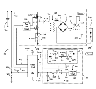
240) which may in turn comprise an output inductor. The output inductor may be
magnetically
coupled to a winding for generating a sense voltage that may be used to
generate a load-current
feedback signal. The load-current feedback signal may have a magnitude
representative of the
magnitude of a load current conducted through the electrical load (e.g., the
load-current feedback
signal VI-LOAD).
[0043] The control circuit may execute the second load current measurement
procedure 600,
for example, periodically at 610 (e.g., when a target power level of the
electrical load is below a low
threshold). In addition, the second load current measurement procedure 600 may
be executed as part
of another load current measurement procedure. At 612, the control circuit may
drive a filter control
signal (e.g., the filter control signal VFc) high to enable a filter circuit
(e.g., a boxcar filter circuit) to
adjust the magnitude of the load-current feedback signal. At 614, the control
circuit may wait for a
time period (e.g., the filter window time period TFw as shown in Fig. 4),
before driving the filter
control signal low to disable the filter circuit from adjusting the magnitude
of the load-current
feedback signal at 616. At 618, the control circuit may determine the average
magnitude of the load
current ILOAD, e.g., by sampling and processing (e.g., scaling) the magnitude
of the load-current
feedback signal VI-LOAD.
[0044] Fig. 7 is a simplified flowchart of a third load current
measurement procedure 700
that may be executed by a control circuit of a load control device (e.g., the
control circuit 150 of the
CA 03108185 2021-01-29
WO 2020/028398 PCT/US2019/044192
- 20 -
LED driver 100 and/or the control circuit 250 of the LED driver 200) for
controlling an electrical
load (e.g., an LED light source, such as the LED light source 202). For
example, the control circuit
may execute the third load current measurement procedure 600 to determine an
average magnitude
of a load current of the electrical load (e.g., the load current LOAD
described herein) using multiple
load current measurement techniques (e.g., using the first and second load
current measurement
procedures 500, 600 shown in Figs. 5 and 6). The load control device may
comprise a load
regulation circuit (e.g., the load regulation circuit 140 and/or the forward
converter 240).
[0045] The control circuit may execute the third load current measurement
procedure 700,
for example, periodically at 710. For example, if the present intensity LPRES
of the LED light source
is greater than a first threshold intensity LTHi (e.g., approximately 60% of a
maximum intensity of
the LED light source) at 712, the control circuit may determine the average
magnitude of the load
current koAD using a first load current measurement technique at 714, for
example, by executing the
first load current measurement procedure 500 (e.g., as shown in Fig. 5). If
the present intensity
LpREs of the LED light source is less than a second threshold intensity L1H2
(e.g., approximately 40%
of the maximum intensity of the LED light source) at 716, the control circuit
may determine the
average magnitude of the load current koAD using a second load current
measurement technique at
718, for example, by executing the second load current measurement procedure
600 (e.g., as shown
in Fig. 6).
[00461 If the present intensity LPRES of the LED light source is less than
or equal to the first
threshold intensity LT1-11 at 712 and greater than or equal to the second
threshold intensity LTH2 at 716
(e.g., if the present intensity LPRES of the LED light source is between the
first threshold
intensity Lull and the second threshold intensity LTH2), the control circuit
may use both of the first
and second load current measurement techniques and combine the values (e.g.,
scaled versions of the
values) determined from the first and second load current measurement
techniques to determine the
average magnitude of the load current koAD. For example, the control circuit
may determine a first
value koADi for the average magnitude of the load current koAD using the first
load current
measurement technique at 720, and determine a second value ILOAD2 for the
average magnitude of
the load current _LOAD using the second load current measurement technique at
722. At 724, the
CA 03108185 2021-01-29
WO 2020/028398 PCT/US2019/044192
-21 -
control circuit may determine a scaling factor a for calculating the average
magnitude of the load
current ILOAD. For example, the first and second values kOAD1, kOAD2 may be
blended (e.g., linearly
blended) together between the first and second threshold intensities LTH1,
L1E2. The scaling factor a
may represent a percentage distance of the present intensity LPRES between the
first and second
threshold intensities LTH1, Unu, e.g,
a = (LmEs ¨ LTH2) (LTH1 ¨ LTH2).
At 726, the control circuit may calculate the average magnitude of the load
current koAD based on
two components derived using the first and second load current measurement
techniques and by
applying the scaling factor a to those components, e.g.,
'LOAD = a = ILOAD1 (1 ¨ a) = ILOAD2
where a = kokm and (1 ¨ a) = kOAD2 may represent respective portions of koAm,
koAD2 used to
calculate the average magnitude of the load current koAD. After determining
the average magnitude
of the load current koAD at 714, 718, or 726, the third load current
measurement procedure 700 may
exit.
[0047] Although described with reference to an LED driver, one or more
embodiments
described herein may be used with other load control devices. For example, one
or more of the
embodiments described herein may be performed by a variety of load control
devices that are
configured to control of a variety of electrical load types, such as, for
example, a LED driver for
driving an LED light source (e.g., an LED light engine); a screw-in luminaire
including a dimmer
circuit and an incandescent or halogen lamp; a screw-in luminaire including a
ballast and a compact
fluorescent lamp; a screw-in luminaire including an LED driver and an LED
light source; a dimming
circuit for controlling the intensity of an incandescent lamp, a halogen lamp,
an electronic low-
voltage lighting load, a magnetic low-voltage lighting load, or another type
of lighting load; an
electronic switch, controllable circuit breaker, or other switching device for
turning electrical loads
or appliances on and off; a plug-in load control device, controllable
electrical receptacle, or
controllable power strip for controlling one or more plug-in electrical loads
(e.g., coffee pots, space
heaters, other home appliances, and the like); a motor control unit for
controlling a motor load (e.g.,
a ceiling fan or an exhaust fan); a drive unit for controlling a motorized
window treatment or a
projection screen; motorized interior or exterior shutters; a thermostat for a
heating and/or cooling
CA 03108185 2021-01-29
WO 2020/028398 PCT/US2019/044192
- 22 -
system, a temperature control device for controlling a heating, ventilation,
and air conditioning
(HVAC) system; an air conditioner, a compressor; an electric baseboard heater
controller; a
controllable damper; a humidity control unit; a dehumidifier; a water heater;
a pool pump; a
refrigerator; a freezer; a television or computer monitor; a power supply; an
audio system or
amplifier; a generator; an electric charger, such as an electric vehicle
charger; and an alternative
energy controller (e.g, a solar, wind, or thermal energy controller). A single
control circuit may be
coupled to and/or adapted to control multiple types of electrical loads in a
load control system.