Note: Descriptions are shown in the official language in which they were submitted.
CA 03109467 2021-02-11
WO 2020/036597 PCT/US2018/046799
ELECTROMAGNETIC INTERFERENCE RESISTANT ELECTRONICS
ENCLOSURE
Background of the Invention
1. Field of the Invention
The present invention relates to electronics housings, and more particularly,
to an
electronics enclosure having electromagnetic interference resistance.
2. Statement of the Problem
Electronics enclosures that house sensitive electronics may be susceptible to
electromagnetic interference (EMI). EMI is the process by which radiated or
conducted
energy is transmitted to another device and can cause performance and
measurement
deviations. This interference is in the form of radiated energy from natural
(lightning
for example) or man-made (equipment, motors, broadcast antennae, etc). All
electronics
products must meet a minimum standard of EMC (Electromagnetic Compatibility)
that
allows them to operate, under the influence of EMI, without affecting primary
equipment functions. To attenuate the effects of EMI, some form of shielding
is
generally required. Some scheme to absorb and/or reflect EMI energy may be
employed both to confine the EMI energy within a source device, and to
insulate that
device from EMI sources. A circuit, completely surrounded by a metal enclosure
without openings, is shielded from EMI. However, this is generally not a
practical
solution since the circuit must interface with the outside world.
Typically, shielding is provided that is located between the EMI source and
the
electronics, and is usually constructed such that an electrically conductive
and grounded
housing encloses the device, yet provides apertures to allow external
interfacing. These
apertures typically take the form of small holes, doors, panels, etc. When
apertures are
present, however, the shield is interrupted and EMI energy can enter the
enclosure via
conduction (on the wires) or radiation (energy propagated through the
opening). The
amount of interference is based on the aperture size and the radiated
frequency. The
size of the opening and susceptibility to external interference is related to
the external
signal wavelength.
X = c / f (1)
1
CA 03109467 2021-02-11
WO 2020/036597 PCT/US2018/046799
where:
X is the wavelength;
c is the speed of light; and
f is the frequency.
Thus, higher frequencies result in small wavelengths, and even very small
apertures in a shield allow entry of high frequencies. Such apertures are
effectively
shielding disruptions that may even operate as a form of slot antenna to
provide a
secondary source of EMI radiation. In such cases, the amplitude of the noise
is roughly
proportional to the length of the aperture.
There are a number of standard practices to control EMI related to the
presence
of apertures, however all have drawbacks. For example, cable may be shielded
such
that wires are wrapped with conductive material. Unfortunately, wire shielding
is often
user-dependent, and requires that a customer install the needed wire shielding
to
maintain the shield integrity. This is not controllable by a device
manufacturer. In
another example, wires may be enclosed in another "metal extension" that
protrudes
from an enclosure and maintains the wires inside a continuous shield. These
tend to be
extremely expensive and add additional installation costs. Lastly, apertures
may be
controlled in size to eliminate certain frequencies. This, however, is not
always possible
based upon the size and dimension of the housing and its related
configuration.
Furthermore, products that are used in hazardous areas often require
particular spacing
considerations that constrain aperture size adjustment.
Some industrial environments have an explosive atmosphere. A spark of
sufficient energy in these environments can ignite an explosion. One potential
source of
these sparks is circuitry used to perform and monitor certain operations in
these
environments. Some electronic devices, such as industrial measuring
instruments for
example, may generate an electrostatic discharge or spark during their
operation. In
dangerous atmospheres, it is important to enclose such circuits in an
explosion proof
compartment to prevent a spark created inside the compartment from igniting
the
atmosphere outside of the compartment.
Industrial measuring instruments, such as flowmeters, are often operated in
locations in which there is a danger of explosion, i.e., the electronic
apparatus is located
2
CA 03109467 2021-02-11
WO 2020/036597 PCT/US2018/046799
not in normal air, but in a potentially explosive atmosphere. Examples of
environments
in which potentially explosive atmospheres are present or may arise are
refueling
facilities, hydrocarbon capture or transfer facilities, or chemical plants,
for example.
Such electronic apparatuses that are to be usable in hazardous areas are
subject to
special safety regulations, which are defined in a number of operational
standards. The
main objects of those standards are to avoid an electric spark that may
initiate an
explosion, or to prevent a spark produced inside an enclosed space from
causing an
explosion outside, or to ensure that a flame that has already developed will
be confined
to the space in which it has developed. By way of example only, European
Standards
IEC 60079-1, describe the requirements for electronics devices necessary to be
considered an "flameproof enclosure" (Ex-d). Ideally, in the event of a fault
or a short
circuit, the maximum amount of energy released is not sufficient to produce a
spark
capable of causing ignition. These are examples of some European standards,
and are
provided as an example only, but comparable standards exist in the USA,
Canada,
Japan, and other countries.
In particular, electronic apparatuses designed to meet the requirements of Ex-
d
protection must be located in a portion of an enclosure that is explosion
proof. This
prevents an explosion that occurs inside the enclosure from penetrating to the
outside or
to another compartment, e.g., from the electronics compartment to the terminal
compartment.
Flowmeters, such as Coriolis mass flowmeters and vibrating densitometers,
typically operate by detecting motion of a vibrating conduit that contains a
flowing
material. Properties associated with the material in the conduit, such as mass
flow,
density and the like, can be determined by processing measurement signals
received
from motion transducers associated with the conduit. The vibration modes of
the
vibrating material-filled system generally are affected by the combined mass,
stiffness
and damping characteristics of the containing conduit and the material
contained
therein.
A typical Coriolis mass flowmeter includes one or more conduits that are
.. connected inline in a pipeline or other transport system and convey
material, e.g., fluids,
slurries, emulsions, and the like, in the system. Each conduit may be viewed
as having a
set of natural vibration modes, including for example, simple bending,
torsional, radial,
3
CA 03109467 2021-02-11
WO 2020/036597 PCT/US2018/046799
and coupled modes. In a typical Coriolis mass flow measurement application, a
conduit
is excited in one or more vibration modes as a material flows through the
conduit, and
motion of the conduit is measured at points spaced along the conduit.
Excitation is
typically provided by an actuator, e.g., an electromechanical device, such as
a coil-type
driver, that perturbs the conduit in a periodic fashion. Mass flow rate may be
determined by measuring time delay or phase differences between motions at the
transducer locations. Two such transducers (or pickoff sensors) are typically
employed
in order to measure a vibrational response of the flow conduit or conduits,
and are
typically located at positions upstream and downstream of the actuator. The
two pickoff
sensors are connected to electronic instrumentation. The instrumentation
receives
signals from the two pickoff sensors and processes the signals in order to
derive a mass
flow rate measurement, among other things.
For flowmeters, by way of example, an explosion proof physical barrier may
separate the compartments of a fieldmount transmitter housing. Process control
transmitters designed for use in hazardous atmospheres often utilize a
combination of
protection methods, including explosion proof housings and/or barriers, to
avoid
uncontrolled explosions of flammable gases. In the case of Coriolis flowmeter
transmitters, it is well known to enclose the active electronics components
within an
explosion proof compartment, so that an explosion of gases that might occur as
a result
of electrical energy within the electronics will not propagate beyond the
enclosure.
Furthermore, it is sometimes preferred that user-accessible connection
facilities of the
electronics utilize "increased safety" rather than explosion proof as a
protection method,
wherein the connection facilities are shown to be non-sparking and therefore
incapable
of igniting a flammable gas. Under either standard, active electronics which
could cause
ignition are contained in a compartment wherein any ignition within the
compartment
cannot escape the compartment.
An enclosure is therefore provided that provides an EMI shield that utilizes a
PCB to transfer the signals in/out of the enclosure. A continuous shield
against radiated
energy is integrally created with the PCB routed traces. In embodiments, the
enclosure
maintains a flameproof or explosion proof interface.
4
CA 03109467 2021-02-11
WO 2020/036597 PCT/US2018/046799
Summary
An EMI resistant electronics enclosure is provided according to an embodiment.
The EMI resistant electronics comprises a first compartment defined by a body
and a
second compartment defined by the body. A septum is between the first
compartment
and the second compartment. A first aperture with the septum connects the
first
compartment and the second compartment. A feed-through element comprises a
first
interface region and a second interface region, wherein one or more primary
conductors
extend between the first interface region and the second interface region, and
wherein
the first interface region resides in the first compartment, and the second
interface
region resides in the second compartment. A conductive bar circumscribes at
least a
portion of the feed-through element, and a conductive gasket extends from the
body to
the conductive bar, wherein a ground path is formed between the body and the
conductive bar with the conductive gasket.
A method of forming an EMI resistant electronics enclosure is provided
according to an embodiment. The method comprises providing a body comprising a
first compartment and a second compartment, and separating the first
compartment and
the second compartment with a septum. A first aperture is placed in the septum
that
connects the first compartment and the second compartment. A feed-through
element is
inserted through the first aperture and cavity, wherein the feed-through
element
comprises a first interface region and a second interface region, wherein one
or more
primary conductors extend between the first interface region and the second
interface
region, and wherein the first interface region resides in the first
compartment, and the
second interface region resides in the second compartment. A conductive bar is
placed
around at least a portion of the feed-through element, and a conductive gasket
is
installed between the body and the conductive bar, to form a conductive path
therebetween.
Aspects
According to an aspect, an EMI resistant electronics enclosure comprises a
first
compartment defined by a body and a second compartment defined by the body. A
septum is between the first compartment and the second compartment. A first
aperture
with the septum connects the first compartment and the second compartment. A
feed-
5
CA 03109467 2021-02-11
WO 2020/036597 PCT/US2018/046799
through element comprises a first interface region and a second interface
region,
wherein one or more primary conductors extend between the first interface
region and
the second interface region, and wherein the first interface region resides in
the first
compartment, and the second interface region resides in the second
compartment. A
conductive bar circumscribes at least a portion of the feed-through element,
and a
conductive gasket extends from the body to the conductive bar, wherein a
ground path is
formed between the body and the conductive bar with the conductive gasket.
Preferably, the electronics enclosure comprises a flexible member comprising
secondary internal conductors that are in electrical communication with the
primary
conductors, and an EMI shield formed as an outer layer of the flexible member
that
surrounds the secondary conductors of the flexible member.
Preferably, the feed-through element comprises a printed circuit board.
Preferably, the gasket comprises a conductive fabric.
Preferably, the EMI shield is in electrical contact with the conductive bar.
Preferably, the EMI shield is in electrical contact with a secondary PCB
disposed
in the second compartment.
Preferably, the secondary PCB comprises a conductive connection point, wherein
the conductive connection point is in electrical contact with the EMI shield.
Preferably, the conductive connection point is grounded.
According to an aspect, a method of forming an EMI resistant electronics
enclosure comprises providing a body comprising a first compartment and a
second
compartment, and separating the first compartment and the second compartment
with a
septum. A first aperture is placed in the septum that connects the first
compartment and
the second compartment. A feed-through element is inserted through the first
aperture
and cavity, wherein the feed-through element comprises a first interface
region and a
second interface region, wherein one or more primary conductors extend between
the
first interface region and the second interface region, and wherein the first
interface
region resides in the first compartment, and the second interface region
resides in the
second compartment. A conductive bar is placed around at least a portion of
the feed-
through element, and a conductive gasket is installed between the body and the
conductive bar, to form a conductive path therebetween.
6
CA 03109467 2021-02-11
WO 2020/036597 PCT/US2018/046799
Preferably, the method comprises electrically connecting secondary internal
conductors of a flexible member to the primary conductors, and surrounding the
secondary conductors of the flexible member with an EMI shield.
Preferably, the feed-through element comprises a printed circuit board.
Preferably, the gasket comprises a conductive fabric.
Preferably, the method comprises the step of placing the EMI shield in
electrical
contact with the conductive bar.
Preferably, the method comprises the step of electrically connecting the EMI
shield with a secondary PCB disposed in the second compartment.
Preferably, the method comprises the step of placing a conductive connection
point of the secondary PCB in electrical contact with the EMI shield.
Description of the Drawings
The same reference number represents the same element on all drawings. The
drawings are not necessarily to scale.
FIG. 1 shows a vibratory flowmeter according to an embodiment of the
invention;
FIG. 2 illustrates an embodiment of an EMI resistant electronics enclosure;
FIG. 3 is an isometric view of the EMI resistant electronics enclosure of FIG.
2
with cap members omitted;
FIG. 4 and 5 illustrate magnified isometric views of the EMI resistant
electronics
enclosure of FIGS. 2 and 3;
FIG. 6 illustrates the magnified isometric views of the EMI resistant
electronics
enclosure of FIG. 5 without a gasket installed;
FIG. 7 illustrates a side view of the EMI resistant electronics enclosure of
FIGS.
2-5; and
FIG. 8 illustrates a cross-sectional view of an embodiment of an EMI resistant
electronics enclosure.
Detailed Description
FIGS. 1-8 and the following description depict specific examples to teach
those
skilled in the art how to make and use the best mode of the invention. For the
purpose
7
CA 03109467 2021-02-11
WO 2020/036597 PCT/US2018/046799
of teaching inventive principles, some conventional aspects have been
simplified or
omitted. Those skilled in the art will appreciate variations from these
examples that fall
within the scope of the invention. Those skilled in the art will appreciate
that the
features described below can be combined in various ways to form multiple
variations
of the invention. As a result, the invention is not limited to the specific
examples
described below, but only by the claims and their equivalents.
FIG. 1 shows a vibratory flowmeter 5 according to the invention. The explosion
proof feedthrough described herein is contemplated for use with such a
vibratory
flowmeter 5. However, this is merely an example of an application for the
explosion
proof feedthrough, and is in no way limiting, as the explosion proof
feedthrough may be
utilized with any appropriate device. The vibratory flowmeter 5 comprises a
flowmeter
assembly 10 and meter electronics 20. The meter electronics 20 is connected to
the
meter assembly 10 via leads 100 and is configured to provide measurements of
one or
more of a density, mass flow rate, volume flow rate, totalized mass flow,
temperature, or
other measurements or information over a communication path 26. It should be
apparent to those skilled in the art that the vibratory flowmeter 5 can
comprise any
manner of vibratory flowmeter, regardless of the number of drivers, pick-off
sensors,
flow conduits, or the operating mode of vibration. In some embodiments, the
vibratory
flowmeter 5 can comprise a Coriolis mass flowmeter. In addition, it should be
recognized that the vibratory flowmeter 5 can alternatively comprise a
vibratory
densitometer.
The flowmeter assembly 10 includes a pair of flanges 101a and 101b, manifolds
102a and 102b, a driver 104, pick-off sensors 105a and 105b, and flow conduits
103A
and 103B. The driver 104 and the pick-off sensors 105a and 105b are connected
to the
flow conduits 103A and 103B.
The flanges 101a and 101b are affixed to the manifolds 102a and 102b. The
manifolds 102a and 102b can be affixed to opposite ends of a spacer 106 in
some
embodiments. The spacer 106 maintains the spacing between the manifolds 102a
and
102b in order to prevent pipeline forces from being transmitted to flow
conduits 103A
and 103B. When the flowmeter assembly 10 is inserted into a pipeline (not
shown)
which carries the flow fluid being measured, the flow fluid enters the
flowmeter
assembly 10 through the flange 101a, passes through the inlet manifold 102a
where the
8
CA 03109467 2021-02-11
WO 2020/036597 PCT/US2018/046799
total amount of flow fluid is directed to enter the flow conduits 103A and
103B, flows
through the flow conduits 103A and 103B and back into the outlet manifold
102b,
where it exits the meter assembly 10 through the flange 101b.
The flow fluid can comprise a liquid. The flow fluid can comprise a gas. The
flow fluid can comprise a multi-phase fluid, such as a liquid including
entrained gases
and/or entrained solids.
The flow conduits 103A and 103B are selected and appropriately mounted to the
inlet manifold 102a and to the outlet manifold 102b so as to have
substantially the same
mass distribution, moments of inertia, and elastic modulus about the bending
axes
Wa--Wa and Wb--Wb respectively. The flow conduits 103A and 103B extend
outwardly from the manifolds 102a and 102b in an essentially parallel fashion.
The flow conduits 103A and 103B are driven by the driver 104 in opposite
directions about the respective bending axes Wa and Wb and at what is termed
the first
out of phase bending mode of the vibratory flowmeter 5. The driver 104 may
comprise
one of many well known arrangements, such as a magnet mounted to the flow
conduit
103A and an opposing coil mounted to flow conduit 103B. An alternating current
is
passed through the opposing coil to cause both conduits to oscillate. A
suitable drive
signal is applied by the meter electronics 20 to the driver 104 via the lead
110. Other
driver devices are contemplated and are within the scope of the description
and claims.
The meter electronics 20 receives sensor signals on the leads 111a and 111b,
respectively. The meter electronics 20 produces a drive signal on the lead 110
which
causes the driver 104 to oscillate the flow conduits 103A and 103B. Other
sensor
devices are contemplated and are within the scope of the description and
claims.
The meter electronics 20 processes the left and right velocity signals from
the
pick-off sensors 105a and 105b in order to compute a flow rate, among other
things.
The communication path 26 provides an input and an output means that allows
the
meter electronics 20 to interface with an operator or with other electronic
systems. The
description of FIG. 1 is provided merely as an example of the operation of a
Coriolis
flowmeter and is not intended to limit the teaching of the present invention.
The meter electronics 20 in one embodiment is configured to vibrate the
flowtubes 103A and 103B. The vibration is performed by the driver 104. The
meter
electronics 20 further receives resulting vibrational signals from the pickoff
sensors
9
CA 03109467 2021-02-11
WO 2020/036597 PCT/US2018/046799
105a and 105b. The vibrational signals comprise vibrational responses of the
flowtubes
103A and 103B. The meter electronics 20 processes the vibrational responses
and
determines a response frequency and/or phase difference. The meter electronics
20
processes the vibrational response and determines one or more flow
measurements,
including a mass flow rate and/or density of the flow fluid. Other vibrational
response
characteristics and/or flow measurements are contemplated and are within the
scope of
the description and claims.
In one embodiment, the flowtubes 103A and 103B comprise substantially U-
shaped flowtubes, as shown. Alternatively, in other embodiments, the flowtubes
can
comprise substantially straight flowtubes or can comprise one or more
flowtubes of
curved shapes other than U-shaped flowtubes. Additional flowmeter shapes
and/or
configurations can be used and are within the scope of the description and
claims.
FIG 2. is a view of an electronics enclosure 200 according to an embodiment of
the invention. The electronics enclosure 200 may be installed on a flowmeter 5
for
example. It should be clear, however, that the electronics enclosure 200 may
be utilized
in any application where an electronics enclosure 200 is contemplated. The
electronics
enclosure 200 comprises a first access point 201 and a second access point
202. These
access points 201, 202 provide means to access the interior spaces of the
electronics
enclosure 200. In an embodiment, the access points 201, 202 may comprise cap
.. members 203 that are secured to the body 205 of the electronics enclosure
200. In an
embodiment, at least one of the cap members may be transparent so that
interior
electronics and/or a display may be visible to a user.
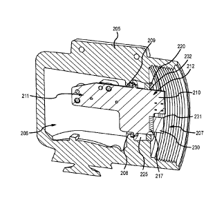
FIG 3. is a view of the electronics enclosure 200 with the cap members 203
removed, according to an embodiment of the invention. The electronics
enclosure 200
in this embodiment includes a feed-through element 210. In an embodiment, the
feed-
through element 210 comprises a substantially planar shape, a first interface
region 211
(see FIG. 8), and a second interface region 212, wherein one or more primary
conductors 217 extend between the first interface region 211 and the second
interface
region 212.
Turning to FIGS. 3 through 8, the body 205 of the electronics enclosure 200
defines a first compartment 206 and a second compartment 207. In an
embodiment,
CA 03109467 2021-02-11
WO 2020/036597 PCT/US2018/046799
meter electronics 20 or other types of electronics are disposed in the first
compartment
206, while terminals and/or interfaces are disposed in the second compartment
207.
Turning particularly to FIG. 8, which is cross-section "A" of FIG. 7, a septum
208 separates the first compartment 206 and a second compartment 207. An
aperture
209 between the first interface region 211 and the second interface region 212
allows
communication between the first compartment 206 and a second compartment 207.
The
aperture 209 may comprise an aperture in a barrier, wall, the septum, or any
other
partition between the first compartment 206 and the second compartment 207.
The interface regions 211, 212 may include, define, or receive an electrical
connector or other electrical component.
The first interface region 211 of the feed-through element 210 extends at
least
partially to the first compartment 206 of the electronics enclosure 200. The
second
interface region 212 of the feed-through element 210 extends at least
partially to the
second compartment 207 of the electronics enclosure 200.
The feed-through element 210 may comprise a substantially planar shape in
some embodiments. However, the feed-through element 210 may be formed in any
desired or needed shape. In some embodiments, the second interface region 212
may be
substantially opposite the first interface region 211. However, this is not
required and
the second interface region 212 may be at any position/orientation with
respect to the
first interface region 211.
The feed-through element 210 includes one or more primary conductors 217
extending from the first interface region 211 to the second interface region
212. The
one or more primary conductors 217 may comprise external conductors formed on
an
outer surface of the feed-through element 210. Alternatively, the one or more
primary
conductors 217 may comprise one or more internal conductors formed partially
or
completely within the feed-through element 210. The one or more primary
conductors
217 may conduct electricity and/or electrical signals between the first
interface region
211 and the second interface region 212.
The feed-through element 210 may comprise an electrical insulator material.
The feed-through element 210 may comprise a non-flammable or flame or heat-
resistant
material. In some embodiments, the feed-through element 210 may comprise a
printed
circuit board (PCB). The one or more primary conductors 217 may be formed on
11
CA 03109467 2021-02-11
WO 2020/036597 PCT/US2018/046799
outside surfaces of the feed-through element 210 or may be located partially
or
completely inside the feed-through element 210. The ends of the one or more
primary
conductors 217 at the first interface region 211 are exposed to be
electrically contacted
or coupled. Similarly, the ends of the one or more primary conductors 217 at
the second
interface region 212 are likewise exposed to be electrically contacted or
coupled.
In some embodiments, the feed-through element 210 may be at least partially
flexible. For example, in some embodiments the feed-through element 210 may
comprise a flexible member that is similar to a ribbon cable.
A cavity 225 is disposed proximate the aperture 209. When the feed-through
element 210 is installed in the electronics enclosure 200, the feed-through
element 210
passes through the aperture 209 and the cavity 225. The cavity 225 thus opens
to the
aperture 209 and to the second compartment 207. The cavity 225 may be sealed
by
injecting a potting material therein, also surrounding and embedding the feed-
through
element 210 therein. The potting material prevents a spark, flame, or
explosion from
passing between the first and second compartments 206, 207.
In some embodiments, compliance with a flame proof standard may require
maintaining a small gap, a long flame path length, or both. The flame path
length may
be selected so that a flame may not propagate from one side of the electronics
enclosure
200 to the other side with sufficient heat or energy content to cause
ignition, given a gap
between the feed-through element 210 and the body 205.
In some embodiments, it is desired that gaps do not exist, as gaps may allow
gasses to leak therethrough, and may allow possible gas ignition. Since gaps
may allow
ignition products to propagate through the joint, both the feed-through
element 210 and
aperture 209 may be smooth and regular, i.e., to within a predetermined
surface finish.
Potting material is an epoxy, plastic, or other filling material which seals
the
cavity 225, thus preventing a flame or explosion from escaping through the
cavity 225
or aperture 209.
As part of the assembly process, the feed-through element 210 is disposed in
the
aperture 209, such that the feed-through element 210 is inserted through the
aperture
209 and the cavity 225, wherein the one or more primary conductors 217 extend
between the first interface region 211 and the second interface region 212,
and wherein
the first interface region 211 resides in the first compartment 206, and the
second
12
CA 03109467 2021-02-11
WO 2020/036597 PCT/US2018/046799
interface region 212 resides in the second compartment 207. The potting
material is
then placed in the cavity 225, and takes the shape of the cavity 225, and is
allowed to
cure or harden. The feed-through element 210 is thus retained in the cavity
225 and the
aperture 209 with the potting.
In an embodiment, the feed-through element 210 is inserted through the
aperture
209 and the cavity 225 via the first compartment 206. In an embodiment, the
feed-
through element 210 is inserted through the aperture 209 and the cavity 225
via the
second compartment 207.
In an embodiment, the feed-through element 210 may be machined to a
.. predetermined profile tolerance, wherein the junction between the feed-
through element
210 and the aperture 209 mates with sufficient precision to create a
substantially
explosion proof interface. For example, the feed-through element 210 may be
manufactured to be thicker than desired and then the feed-through element 210
may be
planed, milled, etched, ground, or otherwise processed until the electronics
enclosure
200 comprises a junction between the feed-through element 210 and the aperture
209
having a desired size and shape and desired uniformity. The feed-through
element 210
and/or the aperture 209 may be manufactured to achieve one or more of a
predetermined
perimeter size, a predetermined perimeter shape, and/or a predetermined
perimeter
surface smoothness and/or uniformity. In an embodiment, the feed-through
element 210
overlaps the aperture 209 completely on one of the sides of the aperture 209,
with no
portions of the aperture remaining uncovered, such that the feed-through
element 210
acts as a stop to achieve a predetermined position in the aperture 209.
In order to provide EMI shielding, a gasket 220 is provided. The gasket 220 is
conductive, and provides a ground path. The gasket 220 contacts the body 205,
which is
grounded. The gasket 220 may be secured to the body 205 with an interference
fit. In
embodiments, the gasket 220 may be secured to the body 205 with fasteners
and/or
electrically conductive adhesives. FIG. 6 illustrates the body 205 with the
gasket 220
not installed, while FIG. 5 illustrates the body 205 with the gasket 220
installed. In an
embodiment, the gasket 200 abuts a case edge 221.
In an embodiment, the gasket 220 may be constructed having a relatively
uniform composition. In an embodiment, the gasket 220 may be constructed
having a
core element with gap-filling capabilities which is either filled, sheathed,
or coated with
13
CA 03109467 2021-02-11
WO 2020/036597
PCT/US2018/046799
an electrically conductive element. The core element, may be foamed, un-
foamed, solid,
tubular, and may comprise an elastomeric thermoplastic material such as
polyethylene,
polyurethane, polypropylene, polyvinyl chloride, or a polypropylene-EPDM
blend, or a
thermoplastic or thermosetting rubber such as a butadiene, styrene-butadiene,
nitrile,
chlorosulfonate, neoprene, urethane, or silicone rubber, for example without
limitation,
as other compositions may be utilized. Conductive materials for the filler,
sheathing, or
coating include metal or metal-plated particles, conductive fabrics,
conductive meshes,
and conductive fibers. Metals may include copper, nickel, silver, aluminum,
tin or an
alloy such as Monel, with fibers and fabrics including natural or synthetic
fibers such as
cotton, wool, silk, cellulose, polyester, polyamide, nylon, and polyimide, for
example
without limitation. Alternatively, other conductive particles and fibers such
as carbon,
graphite, or conductive polymer materials may be utilized. In an embodiment,
at least
one layer of a conductive polyester fabric is provided that covers at least
one layer of a
core element.
In an embodiment, the primary conductors 217 electrically exit from the feed-
through element 210 via a flexible member 230, such as a ribbon cable for
example
without limitation. The flexible member 230 comprises internal traces, wires,
or other
secondary conductors (not visible) that are in electrical communication with
the primary
conductors 217. An outer layer of the flexible member 230 comprises an EMI
shield
231. The EMI shield 231 is a conductive layer. In an embodiment, the EMI
shield 231
is grounded to the body 205. In an embodiment, the flexible member 230
connects to a
secondary PCB 240. The secondary PCB is grounded to the body 205 at a
conductive
connection point 241. Furthermore, internal ground conductors (not visible) in
the
secondary PCB 240 provide electrical communication, and thus a ground path,
between
the conductive connection point 241 and the EMI shield 231 of the flexible
member
230. Customer wiring terminals 242 are in electrical communication with the
secondary
conductors of the flexible member 230 via internal conductors of the secondary
PCB
(not visible), and these internal conductors are also shielded against EMI.
A conductive bar 232 is placed on the feed-through element 210. The conductive
bar 232 is disposed 360 around the feed-through element 210. The conductive
bar 232
thus creates a perimeter around the feed-through element 210. The conductive
bar 232
is in electrical contact with the EMI shield 231of the flexible member 230 and
gasket
14
CA 03109467 2021-02-11
WO 2020/036597 PCT/US2018/046799
220. The conductive bar may be made from a metal, such as copper, gold,
silver,
platinum, or any other conductive material known in the art. The gasket 220
may be
secured to the conductive bar 232 with an interference fit. In embodiments,
the gasket
220 may be secured to the conductive bar 232 with fasteners and/or
electrically
conductive adhesives.
When the gasket 220 is installed, it contacts the conductive bar 232, such
that the
conductive bar 232 is in electrical contact with the gasket. Thus, a grounding
path is
created that extends from the housing 205, to the gasket 220, to the
conductive bar 232,
to the EMI shield 231, to the internal conductors in the secondary PCB 240,
and to the
body 205 again via the conductive connection point 241. Therefore, the
conductors in
the feed-through element 210 are fully surrounded by EMI shielding (i.e. the
body 205)
when in the first compartment 206, and still surrounded by EMI shielding in
the second
compartment 207, due to the gasket 220, conductive bar 232, and the EMI shield
231,
since the EMI shield 231 surrounds the internal traces or wires of the
flexible member
230, which are the electrical continuation of the conductors in the feed-
through element
210. In sum, an EMI shield is created that is continuous from the housing 205,
and
extends from electronics internal to the first compartment 206 all the way to
customer
wiring terminals 242 that are in electrical communication with the primary
conductors
217.
In an embodiment, the gasket is installed in the body 205, and the feed-
through
element 210 is installed therein. In another embodiment, the gasket is
installed over the
feed-through element 210, and these elements are subsequently installed in the
body
205.
Overall, EMI shielding is thus provided that creates a 360 continuous shield
around the PCB conductors, and is thus not dependent on customer wiring
practices, yet
still may maintain a flame proof or explosion proof electronics interface. In
an
embodiment, the EMI resistant electronics enclosure conforms to IEC 60079-1.
In an
embodiment, the EMI resistant electronics enclosure conforms to IEC 60079-1
(Ex-d)
for the first compartment 206, and conforms to IEC 60079-7 (Ex-e) for the
second
compartment 207, thus allowing the second compartment's cap member 203 to be
removable.
CA 03109467 2021-02-11
WO 2020/036597 PCT/US2018/046799
The detailed descriptions of the above embodiments are not exhaustive
descriptions of all embodiments contemplated by the inventors to be within the
scope of
the invention. Indeed, persons skilled in the art will recognize that certain
elements of
the above-described embodiments may variously be combined or eliminated to
create
further embodiments, and such further embodiments fall within the scope and
teachings
of the invention. It will also be apparent to those of ordinary skill in the
art that the
above-described embodiments may be combined in whole or in part to create
additional
embodiments within the scope and teachings of the invention. Accordingly, the
scope
of the invention should be determined from the following claims.
16