Note: Descriptions are shown in the official language in which they were submitted.
CA 03109556 2021-02-12
WO 2020/035799
PCT/1132019/056892
PHOTOVOLTAIC DEVICES COMPRISING LUMINESCENT SOLAR
CONCENTRATORS AND PEROVSKITE-BASED PHOTOVOLTAIC
CELLS
DESCRIPTION
The present invention relates to photovoltaic devices (or solar devices)
comprising luminescent solar concentrators (LSCs) and perovskite- based
photovoltaic cells (or solar cells).
More particularly, the present invention relates to a photovoltaic device (or
solar device) comprising: at least one luminescent solar concentrator (LSC)
having an upper surface, a lower surface and one or more external sides; at
least
one perovskite-based photovoltaic cell (or solar cell) positioned on the
outside of
at least one of the external sides of said luminescent solar concentrator
(LSC),
said perovskite being selected from organometal trihalides.
Said photovoltaic device (or solar device) may be used advantageously in
various applications necessitating the production of electrical energy by
utilising
light energy, in particular solar radiation energy such as, for example:
building
integrated photovoltaic (BIPV) systems, photovoltaic windows, greenhouses,
photobioreactors, noise barriers, lighting equipment, design, advertising,
automotive industry. Moreover, said photovoltaic device (or solar device) can
be
used both in stand-alone mode and in modular systems.
Typically, the luminescent solar concentrators (LSCs) known in the art are
in the form of a plate comprising a matrix of a transparent material which, as
such, is transparent to the radiation of interest (for example, transparent
glass
panes or transparent polymeric materials), and one or more photoluminescent
compounds generally selected, for example, from organic compounds, metal
complexes, inorganic compounds (for example, rare earths), quantum dots
(QDs). Due to the effect of the optical phenomenon of total reflection, the
radiation emitted by the photoluminescent compounds is "guided" towards the
thin external sides of said plate, where it is concentrated on photovoltaic
cells (or
solar cells) positioned there. In this way, large surfaces of low-cost
materials
(said plate) can be used to concentrate the light onto small surfaces of high-
cost
CA 03109556 2021-02-12
WO 2020/035799
PCT/1132019/056892
materials [photovoltaic cells (or solar cells)]. Said photoluminescent
compounds
can be deposited on the matrix of transparent material in the form of a thin
film,
or they can be dispersed within the transparent matrix. Alternatively, they
can be
dispersed within the transparent matrix. Alternatively, the transparent matrix
can
be directly functionalised with photoluminescent chromophore groups.
At the state of the art, the performances of luminescent solar concentrators
(LSCs) depends on various factors, the most relevant being, for example, both
the efficiency of conversion of the photoluminescent compounds used that
absorb photons at lower wavelengths and convert them into photons of greater
wavelength, and the efficiency of the photovoltaic cells (or solar cells)
positioned on the external sides of the plate, which convert the latter into
electrical energy. The more able the photovoltaic cells (or solar cells) are
to
utilise the energy of the photons emitted by the photoluminescent compounds in
the conversion into electrical energy, the greater will be the efficiency of
the
photovoltaic device (or solar device).
At the present time, the photovoltaic cells (or solar cells) most often used
together with luminescent solar concentrators (LSCs) are the inorganic ones,
in
particular, photovoltaic cells (or solar cells) based on crystalline silicon
which, in
conditions of direct solar irradiation, give the best performance/production
cost
ratio.
However, because photovoltaic cells (or solar cells) based on crystalline
silicon generally have both low band-gap values (i.e. low values for the
energy
difference between the conduction band and the valency band) (for example,
band-gap values ranging from about 1. 0 eV to about 1.1 eV) and low values for
the open-circuit voltage (Voc) [for example, values for the open-circuit
voltage
(Voc) ranging from about 0.5 V to 0.6 V], said photovoltaic cells (or solar
cells)
based on crystalline silicon do not permit the best use of the radiation
emitted by
the luminescent solar concentrators (LSCs) (generally ranging from 1.5 eV to
2.0
eV).
The coupling of luminescent solar concentrators (LSCs) with photovoltaic
cells (or solar cells) different from those based on crystalline silicon, has
been
described in the literature.
2
CA 03109556 2021-02-12
WO 2020/035799
PCT/1132019/056892
For example, it is known the coupling of luminescent solar concentrators
(LSCs) with inorganic solar cells based on gallium arsenide (GaAs) or gallium
and indium phosphide (InGaP) as reported, for example, by Debjie M. G. et al.,
in "Advanced Energy Materials" (2012), Vol. 2, pag. 12-35.
Koeppe R. et al., in "Applied Physics Letters" (2007), Vol. 90, 181126,
report the coupling of luminescent solar concentrators (LSCs) with organic
solar
cells based on zinc phthalocyanine and fullerene C60.
McKenna B. et al., in "Advanced Materials" (2017), 1606491, report the
use of luminescent solar concentrators (LSCs) with various types of solar
cells
such as, for example, solar cells based on crystalline silicon, solar cells
based on
gallium arsenide (GaAs), perovskite-based solar cells, organic solar cells,
dye-
sensitised solar cells (DSSCs). In particular, perovskite-based solar cells
are
reported, the surface of which is coated with a layer of luminescent material
for
the purpose of improving their stability to ultraviolet radiation.
Chander N. et al., in "Applied Physics Letters" (2014), Vol. 105, 33904,
report a simple method for improving stability to ultraviolet radiation in
perovslcite-based solar cells using a transparent layer of luminescent
material
based on a phosphorus of nanometric dimensions (nano-phosphor), i.e. based on
YV04:Eu3 obtained by hydrothermal treatment, as coating. The above-
mentioned layer is also said to allow an improvement in the efficiency of said
perovskite-based solar cells in terms of power conversion efficiency (PCE).
Hou X. et al., in "Solar Energy Materials & Solar Cells" (2016), Vol. 149,
pag. 21-127, report high-performance perovskite-based solar cells in which a
phosphorus of nanometric dimensions (nanophosphor) is incorporated in the
mesopomus layer of titanium dioxide, i.e. ZnGa204:Eu31. The above-mentioned
perovskite-based solar cells are said to show an improvement both in terms of
power conversion efficiency (PCE) and in terms of short-circuit photocurrent
density (Jsc).
Bella F. et al., in "Science" (2016), Vol. 354(6309), pag. 203-206, report
perovskite-based solar cells having improved performances and stability to
ultraviolet radiation and water, thanks to a coating based on fluorinated
photopolymers.
3
CA 03109556 2021-02-12
WO 2020/035799
PCT/1132019/056892
American patent US 8,952,239 relates to a solar module comprising
various solar concentrators. In one embodiment, a solar module includes a
series
of photovoltaic cells and a solar concentrator coupled to said series of
photovoltaic cells. Said photovoltaic cells may be crystalline silicon-based
or
based on amorphous silicon, germanium, inorganic materials or semiconductor
materials of groups III-V, such as gallium arsenide.
American patent application US 2014/0283896 relates to a transparent
luminescent solar concentrator (LSC). In particular, said luminescent solar
concentrator ( LSC) has luminophores incorporated in a waveguide matrix which
selectively absorbs and emits light in the near infrared to a photovoltaic
array
mounted on the edge of said luminescent solar concentrator (LSC) or
incorporated in said luminescent solar concentrator (LSC). Said photovoltaic
array may also comprise perovskite-based solar cells.
International patent application WO 2015/079094 relates to a solar
concentrator characterised in that it comprises: a transparent or semi-
transparent
substrate; a coating of photonic crystals; at least one photovoltaic cell
placed on
said substrate, the active surface of said at least one photovoltaic cell
being
placed in parallel to said substrate; and a layer of luminescent material
placed in
contact with said coating of photonic crystals, wherein said coating of
photonic
crystals is placed on said substrate and the layer of luminescent material is
placed on said coating of photonic crystals, or said layer of luminescent
material
is placed on said substrate and the coating of photonic crystals is placed on
said
layer of luminescent material. Perovskite-based solar cells are also cited
among
the photovoltaic cells that can be used for this purpose.
However, from the prior art mentioned above, it can be seen that the
coupling of luminescent solar concentrators (LSCs) with perovskite-based
photovoltaic cells (or solar cells) is not specifically described and/or
exemplified.
Perovskite-based photovoltaic cells (or solar cells) are relatively new
entrants into solar photovoltaic technologies and have witnessed a very great
improvement in power conversion efficiency within a very short time. In
particular, in only five years, from 2012 to 2016, perovskite-based
photovoltaic
4
CA 03109556 2021-02-12
WO 2020/035799
PCT/1132019/056892
cells (or solar cells) have passed from a power conversion efficiency of
around
4% up to 22.1% as demonstrated on the following Internet site:
https://www.nrel.gov/pv/assetsiimages/efficiency-chart.png. The type of
perovskite-based photovoltaic cells (or solar cells) widely used in the
photovoltaics (or solar energy) field is the hybrid organic-inorganic one
based on
an organometal halide material characterised by high extinction coefficients
and
charge mobility. The perovskite structure is generally represented by the
formula
ABX3 and, in the case of said organometal halide material, A represents an
organic cation, B represents a metal cation, and X represents a halogen anion.
In
particular, the type of perovskite most often used currently is that based on
lead
halides, wherein A (the organic cation) is methylammonium CH3NH3+, B (the
metal cation) is the lead ion Pb24- and X (the halogen anion) is the tri-
iodide ion I-
, so that the overall formula is CH3NH3Pbb. The bandgap of said type of
perovskite is equal to 1.57 eV, corresponding to a wavelength of about 790 nm
and therefore succeeding in absorbing the whole of the visible spectrum.
Moreover, perovskite-based photovoltaic cells (or solar cells) are easy to
produce and use common materials and are therefore also advantageous
economically. More specifically, said perovskite-based photovoltaic cells (or
solar cells) combine crystallinity and high charge transfer [both of electrons
(-)
and of electron gaps (or holes) (+)} found in inorganic semiconductors, with
the
low-cost production of photovoltaic cells (or solar cells) based on low-
temperature processes in the presence of solvent. Furthermore, unlike
conventional semiconductor photovoltaic cells (or solar cells), perovskite-
based
photovoltaic cells (or solar cells) are able, by varying the type of atoms in
their
crystalline structure, to emulate the bandgap, and therefore the capacity to
absorb
in particular portions of the solar spectrum. On the other hand, said
perovskite-
based photovoltaic cells (or solar cells) exhibit an external quantum
efficiency
(EQE) that is lower than the external quantum efficiency (EQE) of photovoltaic
cells (or solar cells) based on crystalline silicon.
Further details about perovskite-based photovoltaic cells (or solar cells)
may be found, for example, in: Cui J. et al., "Science and Technology of
Advanced Materials" (2015), Vol. 16, 036004; Eperon G. E. et al., "Energy &
CA 03109556 2021-02-12
WO 2020/035799
PCT/1132019/056892
Environmental Science" (2014), Vol. 7, pag. 982-988; Li G. et al., "Advanced
Energy Materials" (2015), 1401775.
The study of photovoltaic devices (or solar devices) comprising
luminescent solar concentrators (LSCs) and perovskite-based photovoltaic cells
(or solar cells) is therefore of great interest.
The Applicant therefore posed the problem of discovering a photovoltaic
device (or solar device) comprising luminescent solar concentrators (LSCs) and
perovskite-based photovoltaic cell cells (or solar cells) that are capable of
exhibiting good values of electrical power density (p) and, consequently, good
performances.
The Applicant has now discovered a perovskite-based photovoltaic cell (or
solar cell) comprising at least one luminescent solar concentrator (LSC) and
at
least one perovskite-based photovoltaic cell (or solar cell) that are capable
of
exhibiting good values of electrical power density (p) and, consequently, good
performances. Furthermore, said photovoltaic device (or solar device) exhibits
a
ratio between the electrical power density (p) generated and the electrical
power
density expected (
xPexpected), calculated as reported below, greater than 1 and,
consequently, a greater generated electrical power density (p) with respect to
that
expected. Said photovoltaic device (or solar device) may be used
advantageously
in various applications necessitating the production of electrical energy by
utilising light energy, in particular solar radiation energy such as, for
example:
building integrated photovoltaic (BIPV) systems, photovoltaic windows,
greenhouses, photobioreactors, noise barriers, lighting equipment, design,
advertising, automotive industry. Moreover, said photovoltaic device (or solar
device) can be used both in stand-alone mode and in modular systems.
The object of the present invention is therefore a photovoltaic device (or
sobs device) comprising:
at least one luminescent solar concentrator (LSC) having an upper surface,
a lower surface and one or more external sides;
at least one perovskite-based photovoltaic cell (or solar cell) positioned
outside of at least one of the external sides of said luminescent solar
concentrator (LSC), said perovskite being selected from organometal
6
CA 03109556 2021-02-12
WO 2020/035799
PCT/1132019/056892
trihalicies.
For the purpose of the present description and of the claims which follow,
unless otherwise specified the definitions of the numerical ranges always
comprise the extremes.
For the purpose of the present description and of the claims which follow,
the term "comprising" also includes the terms "that consists essentially of'
or
"that consists of'.
As mentioned above, said luminescent solar concentrator usq has an
upper surface, a lower surface and one or more external sides. According to
one
embodiment, said luminescent solar concentrator (LSC) may have one external
side (e.g., it may be circular), three, four, five, six, seven, or more sides.
According to one embodiment, said luminescent solar concentrator (LSC) may
have a lower surface distanced from the upper surface, wherein the external
side(s) extends/extend from the upper surface to the lower one. According to
one
embodiment, said upper surface is configured to receive photons from a photon
source and is positioned closer to the photon source with respect to said
lower
surface.
According to a preferred embodiment of the present invention, said
luminescent solar concentrator (LSC) has an upper surface configured to
receive
the photons, a lower surface configured to receive the photons, said upper
surface being positioned closer to the photon source with respect to the lower
surface, and four external sides that extend from the upper surface to the
lower
one.
According to a preferred embodiment of the present invention, said
luminescent solar concentrator (LSC) is a plate comprising a matrix in
transparent material and at least one photoluminescent compound.
According to a preferred embodiment of the present invention, said
transparent material may be selected, for example, from: transparent polymers
such as, for example, polymethyl methacrylate (PMMA), polycarbonate (PC),
polyisobutyl methacrylate, polyethyl methacrylate, polyallyl diglycol
carbonate,
polymethacrylimide, polycarbonate ether, polyethylene terephthalate, polyvinyl
butyral, ethylene-vinylacetate copolymers, ethylene-tetafluoroethylene
7
CA 03109556 2021-02-12
WO 2020/035799
PCT/I132019/056892
copolymers, polyimide, polyurethane, styrene-acrylonitrile copolymers, styrene-
butadiene copolymers, polystyrene, methyl-methacrylate styrene copolymers,
polyethersulfone, polysulfone, cellulose triacetate, transparent and impact-
resistant crosslinIced acrylic compositions consisting of a fragile matrix (I)
having a glass transition temperature (TO above 0 C and elastomeric domains
having dimensions smaller than 100 nm which consist of macmmolecular
sequences (H) having a flexible nature with a glass transition temperature
(Tg)
below 0 C and described, for example, in american patent application US
2015/0038650 (hereinafter referred to, for greater simplicity, as PPMA-1R), or
mixtures thereof; transparent glass such as, for example, silica, quartz,
alumina,
titanium dioxide, or mixtures thereof. Polynnethylmethacrylate (PMMA),
PMMA-1R, or mixtures thereof, are preferred. Preferably, said transparent
material may have a refractive index ranging from 1.30 to 1.70.
According to a preferred embodiment of the present invention, said
photoluminescent compound may be selected, for example, from: perylene
compounds such as, for example, compounds known with the commercial name
of Lumogen from BASF; acene compounds described, for example, in
international patent application WO 2011/048458 in the name of the Applicant;
benzothiadiazole compounds described, for example, in international patent
application WO 2011/048458 in the name of the Applicant; compounds
comprising a benzoheterodiazole group and at least one benzodithiophene group
described, for example, in international patent application WO 2013/098726 in
the name of the Applicant; disubstituted naphtathiadiazole compounds
described,
for example, in European patent application EP 2 789 620 in the name of the
Applicant; benzoheterodiazole compounds disubstituted with benzodithiophene
groups described, for example, in European patent application EP 2 789 620 in
the name of the Applicant; disubstituted benzoheterodiazole compounds
described, for example, in international patent application WO 2016/046310 in
the name of the Applicant; disubstituted diaryloxybenzoheterodiazole
compounds described, for example, in international patent application WO
2016/046319 in the name of the Applicant; or mixtures thereof.
Specific examples of photoluminescent compounds that may
8
CA 03109556 2021-02-12
WO 2020/035799
PCT/1132019/056892
advantageously be used for the purpose of the present invention are: 1V,N' -
bis(2' ,6' -di-iso-propylphenyl)(1,6,7 ,12-tetraphenoxy)(3,4,9,10-perylene
diimide
(Lurnogen F Red 305 - Bast), 9,10-diphenylanthracene (DPA), 4,7-di(thien-2'-
y1)-2,1,3-benzothiadiazole (DTB), 5,6-dipherioxy-4,7-bis(2-thieny1)-2,1,3-
benzothiadiazole (DTBOP), 5,6-diphenoxy-4,7-bis[5-(2,6-dimethylpheny1)-2-
thienyl]benzo[c]1,2,5-thiadiazole (MPDTBOP), 5,6-diphenoxy-4,7-bis[5-(2,5-
dimethylpheny1)-2-thienyl]benzo[c]1,2,5-thiadiazole (PPDTBOP), 4,7-bis[5-
(2,6-dimethylpheny1)-2-thienyllbenzo[c]1,2,5-thiadiazole (MPDTB), 4,7-bis[5-
(2,6-di-iso-propylpheny1)-2-thienyl]benzo[c]1,2,5-thiadiazole (IPPDTB), 4,7-
bis[4,5-(2,6-dimethylpheny1)-2-thienyl]benzo[c]1,2,5-thiadiazole (2 MPDTB)
4,7-bis(7',8'-dibutylbenzo[1',2'-b':4',3'-b"idithien-5'-y1)-benzo[c]
[1,2,5]thia-
diazole (F500), 4,9-
bis(7',8'-dibutylbenzo[1',2'-b' :4',3 ' -b"] dithien-5 ' -y1)-
naphtho[2,3-c][1,2,5jthiadiazole (F521), 4,7-bis(5-(thiophen-2-yl)thiophen-2-
yl)benzo[c][1,2,5]thiadi azole (QTB), 4,9-
bis(thien-2' -y1)-naphtho[2,3-
c] [1,2,5] thiadiazole (DTN), or mixtures thereof. 9,10-5,6-Diphenoxy-4,7-
bis[5-
(2,6-dimethylpheny1)-2-thienyl]benzo[c]1,2,5-thiadiazole (MPDTBOP), 5,6-
diphenoxy-4,7-bis [5-(2,5-dimethylpheny1)-2-thienylibenzo[c]1,2,5-thiadiazole
(PPDTBOP), N,N'-
bis(2',6'-di-iso-propylphenyl)(1,6,7,12-
tetraphenoxy)(3,4,9,10 -perylene diimide (Lumogen F Red 305 - Bast), or
mixtures thereof, are preferred.
According to a preferred embodiment of the present invention, said
photoluminescent compound may be present in said transparent matrix in a
quantity ranging from 0.1 g per unit of surface area to 3 g per unit of
surface
area, preferably ranging from 0.2 g per unit of surface area to 2.5 g per unit
of
surface area, said unit of surface area being referred to the surface area of
the
matrix in transparent material expressed in m2.
According to a further embodiment of the present invention, said
photoluminescent compound may be selected, for example, from quantum dots
(QDs), which may be composed of different elements that may be selected, for
example, from the elements belonging to groups 12-16, 13-15, 14-16, of the
Periodic Table of the Elements. Preferably, said quantum dots (QDs) may be
selected, for example from: lead sulphide (PbS), zinc sulphide (ZnS), cadmium
9
CA 03109556 2021-02-12
WO 2020/035799
PCT/1B2019/056892
sulphide (CdS), cadmium selenide (CdSe), cadmium telluride (CdTe), silver
(Ag), gold (Au), aluminium (Al), or mixtures thereof.
For the purpose of the present description and of the claims which follow,
the term "Periodic Table of the Elements" refers to the "1UPAC Periodic Table
of the Elements", version dated 8 January 2016, reported on the following
Internet site: https://iupac.org/what-we-do/periodic-table-of-elements/.
Further information relating to said quantum dots (QDs) may be found, for
example, in American patent application US 2011/240960.
According to a preferred embodiment of the present invention, said
photoluminescent compound, when selected from said quantum dots (QDs), may
be present in said transparent matrix in a quantity ranging from 0.05 g per
unit of
surface area to 100 g per unit of surface area, preferably ranging from 0.15 g
per
unit of surface area to 20 g per unit of surface area, said unit of surface
area
being referred to the surface area of the matrix in transparent material
expressed
in m2.
According to a preferred embodiment of the present invention, said
luminescent solar concentrator (LSC) is a plate having a thickness ranging
from
0.1 Am to 50 mm, preferably ranging from 0.5 Am to 20 mm.
The above-mentioned photoluminescent compounds may be used in said
luminescent solar concentrator (LSC), in various forms.
For example, in the case wherein the transparent matrix is of the polymeric
type, said at least one photoluminescent compound may be dispersed in the
polymer of said transparent matrix by, for example, melt dispersion, or
addition
in bulk, and subsequent formation of a plate comprising said polymer and said
at
least one photoluminescent compound, working, for example, in accordance with
the casting technique. Alternatively, said at least one photoluminescent
compound and the polymer of said transparent matrix may be solubilised in at
least one suitable solvent, obtaining a solution that is deposited on a plate
of said
polymer, forming a film comprising said at least one photoluminescent
compound and said polymer, working, for example, by the use of a Doctor
Blade-type film applicator: said solvent is then allowed to evaporate. Said
solvent may be selected, for example, from: hydrocarbons such as, for example,
CA 03109556 2021-02-12
WO 2020/035799
PCT/1132019/056892
1,2-dichloromethane, 1,2-dichlorobenzene, toluene, hexane; ketones such as,
for
example, acetone, acetylacetone; or mixtures thereof.
In the case wherein the transparent matrix is of the vitreous type, said at
least one photoluminescent compound may be solubilised in at least one
suitable
solvent (that can be selected from among those mentioned above), obtaining a
solution that is deposited on a plate of said transparent matrix of vitreous
type,
forming a film comprising said at least one photoluminescent compound
working, for example, by the use of a Doctor Blade-type film applicator: said
solvent is then allowed to evaporate.
Alternatively, a plate comprising said at least one organic
photoluminescent compound and said polymer, obtained as described above
according to the casting technique, may be enclosed between two plates of said
transparent matrix of the vitreous type (sandwich) working according to the
known technique used to prepare double-glazed units in an inert atmosphere.
For the purpose of the present invention, said luminescent solar
concentrator (LSC) may be produced in plate form by addition in bulk and
subsequent casting, as described above: further details may be found in the
examples which follow.
In accordance with a preferred embodiment of the present invention, said
perovskite may be selected, for example, from organometal trihalides having
general formula ABX3, wherein:
A represents an organic cation such as, for example, methylammonium
(CH3NH3+), fonnamidinium [CH(NH2)21, n-butylanunonium (C4H12N4),
tetra-butylammonium (C16H361\r);
- B represents a metallic cation such as, for example, lead (Pb2), tin
(Sn'");
- X represents a halogen ion such as, for example, iodine (0, chlorine
(Cl),
bromine (Bo.
In accordance with a further preferred embodiment of the present
invention, said perovskite may be selected, for example from: methyl ammonium
lead iodide (CH3NH3PbI3), methyl ammonium lead bromide (CH3NH3PbBr3),
methyl ammonium lead chloride (CH3NH3PbC13), methyl ammonium lead iodide
bromide (CH3NH3Pb1x8r3-,), methyl ammonium lead iodide chloride
11
CA 03109556 2021-02-12
WO 2020/035799
PCT/1B2019/056892
(CH3NH3Pb1,C13.,), formamidinium lead iodide [CH(M12)2PbI31,
formamidinium lead bromide [CH(NH2)2PbBr3], formamidinium lead chloride
[CH(Nf12)2PbC13], formamidinium lead iodide bromide [CII(N112)2PbIxIk3-x],
formamidinium lead iodide chloride [CH(NH.2)2MC13-0, n-butyl ammonium lead
iodide (C4Ht2NPbI3), tetra-butyl ammonium lead iodide (Ct6H36NTbI3), n-butyl
ammonium lead bromide (C41112NPbBr3), tetra-butyl ammonium lead bromide
(Ci6H36NPbBr3), methyl ammonium tin iodide (CH3NH3SnI3), methyl
ammonium tin bromide (CH3NH3SnBr3), methyl ammonium tin iodide bromide
(CH3NH3SnIxBr3-x), formamidinium tin iodide [CH(NH2)2SnI3], formamidinium
tin iodide bromide [CH(NI12)2SnI.Br3-], n-butyl ammonium tin iodide
(C41-112NSnI3), tetra-butyl ammonium tin iodide (Ci6H36NSnI3), n-butyl
ammonium tin bromide (C4I-112NSnBr3), tetra-butyl ammonium tin bromide
(C16H36NSnBr3), methyl ammonium tin iodide (CH3NH3SnI3), or mixtures
thereof. Methyl ammonium lead iodide (CH3NH3Pb13) is preferred.
For the purpose of the present invention, said perovskite-based
photovoltaic cell (or solar cell) may be selected from the perovslcite-based
photovoltaic cells (or solar cells) of the prior art.
For the purpose of the present invention, said perovskite-based
photovoltaic cell (or solar cell) comprises:
- a substrate of glass coated with a layer of transparent and
conductive oxide
(TCO), commonly tin oxide doped with fluorine (Sn02:F) (Fluorinated Tin
Oxide - FTO), or indium oxide doped with tin (Indium Tin Oxide - fro)
constituting the anode;
- an
electron transporter layer (Electron Transport Material - ETO) the
purpose of which is to extract the electrons photogenerated by the
perovsldte and transfer them to the anode; this is also called a "blocking
layer" in that it blocks the electron gaps (or holes) and, generally, is a
compact layer of titanium dioxide (Ti02);
-
optionally, a scaffold of mesoporous titanium dioxide (Ti02) the purpose
of which is to provide a larger area of interface with the perovskite,
increasing the efficiency of harvesting of electrons, which must follow a
shorter course, seeing the probability of recombination reduced; it can also
12
CA 03109556 2021-02-12
WO 2020/035799
PCT/1B2019/056892
lengthen the optical path, favouring the absorption of radiation;
a layer of perovskite, preferably of methyl ammonium lead iodide
(CH3NH3PbI3), which is the absorbent layer, methyl ammonium lead
iodide (CH3NH3Pbb), as mentioned above, is the structure most often
used, because it exhibits a high coefficient of absorption over the whole
UV and visible spectrum, a bandgap of 1.57 eV, close to the optimum
value for maximising the conversion efficiency and a considerable distance
for diffusion of the electrons and electron gaps (or holes) (more than 100
nm);
a layer based on a hole transport material (HTM), generally of spiro-
MeOTAD
[2,2',7,7'-tetralds(N,N-di-4-methoxyphenylamine)-9,9%
spirobifluorene];
a metallic contact known as a "back contact", which constitutes the
cathode, generally a layer of gold or silver.
Said perovskite-based photovoltaic cell (or solar cell) may be constructed
by working according to processes known in the art, as described, for example,
by Li G. et al., in Advanced Energy Materials (2015), 1401775, mentioned
above: further details relating to the construction of said perovskite-based
photovoltaic cell (or solar cell) can be found in the examples which follow.
For the purpose of improving adhesion between said at least one
luminescent solar concentrator (LSC) and said at least one perovskite-based
photovoltaic cell (or solar cell), a suitable optical gel may be used.
According to a preferred embodiment of the present invention, said at least
one perovskite-based photovoltaic cell (or solar cell) may be coupled to at
least
one of the external sides of said luminescent solar concentrator (LSC) with
use
of a suitable optical gel. Said optical gel must have a refraction index that
allows
good optical coupling and may be selected, for example, from transparent
silicone oils and fats, epoxy resins.
According to a preferred embodiment of the present invention, the
electrical energy generated by said at least one perovsldte-based photovoltaic
cell (or solar cell) may be transported using a wiring system that is
connected to
said photovoltaic device (or solar device).
13
CA 03109556 2021-02-12
WO 2020/035799
PCT/1B2019/056892
For the purpose of the present invention, one or more perovskite-based
photovoltaic cells (or solar cells) may be positioned outside of at least one
of the
sides of said luminescent solar concentrator (LSC), preferably said perovskite-
based photovoltaic cells (or solar cells) may partially or completely cover
the
outer perimeter of said luminescent solar concentrator (LSC).
For the purpose of the present description and the claims which follow, the
term "outer perimeter" is intended to mean the external sides of said
luminescent
solar concentrator (LSC).
As mentioned above, said photovoltaic device (or solar device) may be
used advantageously in various applications necessitating the production of
electrical energy by utilising light energy, in particular solar radiation
energy
such as, for example: building integrated photovoltaic (BIPV) systems,
photovoltaic windows, greenhouses, photobioreactors, noise barriers, lighting
equipment, design, advertising, automotive industry. Moreover, said
photovoltaic device (or solar device) can be used both in stand-alone mode and
in modular systems.
A further subject of the present invention is therefore the use of said
photovoltaic device (or solar device) in: building integrated photovoltaic
(BIP V)
systems, photovoltaic windows, greenhouses, photobioreactors, noise barriers,
lighting equipment, design, advertising, automotive industry.
The present invention will now be illustrated in greater detail by means of
an embodiment with reference to Figures 1 and 2 below reported.
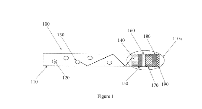
In particular, Figure 1 represents a sectional view with respect to plane (A)
of Figure 2, of a photovoltaic device (or solar device) (100) comprising: a
luminescent solar concentrator (LSC) (110) including at least one
photoluminescent compound (120) and a perovskite-based photovoltaic cell (or
solar cell) (110a) comprising the following layers: a substrate of glass (140)
coated with a layer of transparent and conductive oxide (TCO) (anode) (150);
an
electron transporter layer (Electron Transport Material - ETO) (160); a layer
of
perovskite (170); optionally, a scaffold of mesoporous titanium dioxide (TiO2)
(not shown in Fig. I) positioned between said electron transporter layer
(Electron
Transport Material - ETO) and said perovskite layer (170); a layer based on a
14
CA 03109556 2021-02-12
WO 2020/035799
PCT/1B2019/056892
hole transport material (Hole Transport Material - HTM) (180), a metallic
contact know as a "back contact" (cathode) (190); optionally, a suitable
optical
gel (not shown in Fig. 1) positioned between said substrate layer of glass
(140)
and said luminescent solar concentrator (LSC) (110). In said Figure 1, an
incident photon (130) having a first wavelength enters the luminescent solar
concentrator (LSC) (110) and is absorbed by the photoluminescent compound
(120) and emitted at a second wavelength different from the first. The
incident
photons are internally reflected and refracted within the luminescent solar
concentrator (LSC) until they reach the photovoltaic cell (or solar cell)
(110a)
and are converted into electrical energy.
Figure 2 shows a three-dimensional view of a photovoltaic device (or solar
device) (100) comprising a luminescent solar concentrator (LSC) (110) and a
perovskite-based photovoltaic cell (or solar cell) (110a).
For the purpose of improving understanding of the present invention and
putting it into practice, in what follows we present a number of illustrative
and
non-limiting examples thereof.
For greater simplicity, in the examples which follow the terms "solar cell"
and "solar device" are used, which should be understood as having the same
meaning as "photovoltaic cell" and "photovoltaic device".
EXAMPLE 1
Pleoration of plate 1 (mating).D.ND
In a 4-litre flask were heated, with magnetic stirring, 2500 ml of methyl
methacrylate (MMA) (Sigma-Aldrich), previously distilled in order to remove
any inhibitors of polymerisation, bringing the temperature to 80 C, in 2
hours.
The following were then added: 250 mg 2,2'-azo-bis[2-
methylpropionamidine]dihydrochloride (AIBN) (initiator) dissolved in 250 ml of
methyl methacrylate (MMA) (Sigma-Aldrich), previously distilled: the
temperature of the mixture obtained falls by approximately 3 C - 4 C. Said
mixture was heated, bringing the temperature to 94 C in 1 hour: all this was
left
at said temperature for 2 minutes and then cooled in an ice bath, obtaining a
pre-
polymer syrup which, if not used immediately, may be stored for a few weeks in
a refrigerator.
CA 03109556 2021-02-12
WO 2020/035799
PCT/1B2019/056892
A mould was then prepared, assembled with two glass plates of
dimensions 100x400x6 mm, separated by a seal in polyvinyl chloride (PVC) of
larger diameter equal to 6 mm, held together with metal clamps.
Into a 4-litre glass flask were then added 2 litres of pre-polymer syrup
obtained as described above, 120 mg of lauroyl peroxide (Sigma-Aldrich)
dissolved in 1 litre of methyl methacrylate (MMA) (Sigma-Aldrich), previously
distilled, a quantity of 5,6-diphenoxy-4,7-bis{5-(2,6-dimethylpheny1)-2-
thienylibenzo[c] 1 ,2,5-thiadiazole (MPDTBOP) equal to 200 ppm, 5000 ppm
Tinuvine P (Bast) and 5000 ppm Tinuvin 770 (Basf): the mixture obtained was
maintained with magnetic stirring and under vacuum (10 mm Hg), for 45
minutes, at ambient temperature (25 C), obtaining a degassed solution. The
solution thus obtained was poured into the mould prepared as described above,
which, after closing the seal aperture, was immersed in a bath of water at 55
C,
for 48 hours. The mould was then placed in an oven at 95 C, for 24 hours
(curing step), then removed from the oven and allowed to cool at ambient
temperature (25 C). The metal clamps and the seal were then removed, and the
glass plates were separated by isolating plate 1 (LSC1) (the plate was cut to
dimensions 75x300x6 mm).
EXAMPLE 2
Preparation ofplatt 2 (casting) (LK?)
Plate 2 (LSC2) was prepared by working as reported in Example 1, apart
from the fact that instead of 5,6-diphenoxy-4,7-bis[5-(2,6-dimethylpheny1)-2-
thienyljbenzo[cp,2,5-thiadiazole (MPDTBOP), 5,6-diphenoxy-4,7-bis[5-(2,5-
dimethylpheny1)-2-thienyl]benzo[ci1,2,5-thiadiazole (PPDTBOP) was used in a
quantity equal to 200 ppm, obtaining plate 2 (LSC2) (dimensions 75x300x6
mm).
EXAMPLE 3
Preparation piplate 3 (eastim) (LSC31
Plate 3 (LSC3) was prepared by working as reported in Example 1, apart
from the fact that instead of 5,6-diphenoxy-4,7-bis[5-(2,6-dimethylpheny1)-2-
thienyl]benzo[c]1,2,5-thi adiazole (MPDTBOP), .N,N'-
bis(2',6'-di-iso-
propylphenyl)(1,6,7,12-tetraphenoxy)(3,4,9,10-perilene diimide (Lurnogen F
16
CA 03109556 2021-02-12
WO 2020/035799
PCT/1B2019/056892
Red 305 - Basf) was used in a quantity equal to 160 ppm, obtaining plate 3
(LSC3) (dimensions 75x300x6 mm).
EXAMPLE 4
preparation of perovskite-based solar qell
A perovskite-based solar cell was prepared by following, with a few
modifications, the procedure described by Li G. et al., in Advanced Energy
Materials (2015), 1401775, reported above.
To this end, a pemvskite-based solar cell was prepared on a substrate of
glass coated with FTO [tin oxide doped with fluorine (Sn02:F) - (Fluorinated
Tin Oxide) (Hartford Glass), previously subjected to a cleaning procedure
consisting of cleaning by hand, rubbing with a lint-free cloth soaked in a
detergent diluted with distilled water. The substrate was then rinsed with
distilled
water. The substrate was then deep-cleaned using the following methods in
sequence: ultrasound baths in (i) distilled water plus detergent (followed by
drying by hand with a lint-free cloth; (ii) distilled water [followed by
drying by
hand with a lint-free cloth; (iii) acetone (Aldrich) e (iv) iso-propanol
(Aldrich) in
sequence. In particular, the substrate was placed in a beaker containing the
solvent, placed in an ultrasound bath, maintained at 40 C, for a treatment of
10
minutes. After treatments (iii) and (iv), the substrate was dried in a stream
of
compressed nitrogen.
The glass/FTO was then further cleaned by treating in an ozone device
(UV Ozone Cleaning System EXPO3 - Astel), immediately before proceeding to
the next step.
The thus-treated substrate was ready for deposition of the electron
transporter layer (Electron Transport Material - ETO). To this end, a layer of
compacted titanium dioxide (T102) was deposited by means of reactive
sputtering in a direct current (DC), using titanium dioxide (TiO2) as the
target, in
the presence of argon (Ar) (20 scorn) and of oxygen (02) (4 scorn) on the
substrate. The thickness of the layer of titanium dioxide (TiO2) was equal to
115
nm.
On top of the layer of titanium dioxide (T102) obtained, a layer of
mesoporous titanium dioxide (TiO2) was deposited by working as follows. To
17
CA 03109556 2021-02-12
WO 2020/035799
PCT/1B2019/056892
this end, a solution of a mesoporous titanium dioxide (h02) paste (Dyesol
18NRT - Aldrich) (2 g) in ethanol (Aldrich) (6 g) and terpineol (2 g)
(Aldrich)
was prepared: said solution was deposited by means of spin coating, working at
a
rotation speed of 2000 rpm (acceleration equal to 1000 rpm's), for 45 seconds.
The thickness of the layer of mesoporous titanium dioxide (TiO2) was equal to
600 rim. At the end of deposition, all this was subjected to annealing at 500
C
for 2 hours and then again subjected to cleaning by treating in an ozone
device
(UV Ozone Cleaning System EXPO3 Astel), immediately before proceeding to
the next step.
On top of the layer of mesoporous titanium dioxide (TiO2) thus obtained,
the layer of perovsldte, i.e. the layer of methyl ammonium lead iodide
(CI-13NH3PbI3) was deposited by working as follows: D the lead iodide (Pb12)
(purity 99% - Aldrich) was dissolved in N,N-dimethyl formamide (purity 99.8%
- Aldrich) by working with stirring, at a temperature of 75 C, for 30 minutes,
obtaining a solution at a concentration of lead iodide (Pb12) equal to 462
mg/ml,
said solution was deposited on said mesoporous layer of titanium dioxide
(TiO2)
by means of spin coating, working at a rotation speed of 6000 rpm
(acceleration
equal to 1000 rpm/s), for 90 seconds and all this was dried at 100 C, for 15
minutes; ii) after cooling at ambient temperature, all this was subjected to
dip
coating, for 5 minutes, in a solution of methyl ammonium iodide (MA!)
(CII3NH3I) (purity 98% - Aldrich) in isopropanol (Aldrich) (concentration MAI
equal to 10 mg/m1); iii) spin coating of a solution of methyl ammonium iodide
(MA!) (CH3NH3D (purity 98% - Aldrich) in isopropanol (Aldrich)
(concentration MAI equal to 5 mg/ml), working at a rotation speed of 6000 rpm
(acceleration equal to 1000 rpm/s), for 30 seconds (solar cells in what
follows
indicated as Type A). Regarding the solar cells hereinafter indicated as Type
B,
the solution of methyl ammonium iodide (MAD (CH3NH3I) (purity 98% -
Aldrich) used in step ii) and in step iii) were obtained using said methyl
ammonium iodide (MAI) (CH3NH3l) after crystallization from heptane before
dissolution in isopropanol (concentration of MAI equal to 10 mg/ml). At the
end
of deposition, all this was subjected to desiccation at 100 C for 30 minutes
and
then cooled to ambient temperature (25 C). The thickness of the layer of
18
CA 03109556 2021-02-12
WO 2020/035799
PCT/1132019/056892
perovskite was equal to 300 nm.
On top of the layer of perovskite obtained, a layer based on a hole transport
material (HTM) was deposited. To this end, 72.3 mg spiro-MeOTAD [2,2',7,7'-
tetrakis(N,N-di-4-methoxyphenylamine)-9,9'-spirobifluorene} (Aldrich) was
dissolved in 1 ml chlorobenzene (purity 99.8% - Aldrich) and then 28.8 ill of
4-
tert-butylpyridine (purity 96% -Aldrich) and 17.5 111 of a stock solution at a
concentration equal to 520 mg/ml of lithio-bis(trifluoromethylsulfonyl)imide
(purity 98% - Alfa Aesax) in acetonitrile (purity 99.8% - Aldrich): the
solution
thus obtained was deposited, by means of spin coating, working at a rotation
speed of 2000 rpm (acceleration equal to 500 minis), for 45 seconds. The
thickness of the layer based on hole transport material (HTM) was equal to 150
tun.
On top of said layer based on a hole transport material (HTM) the back
contact (cathode) of gold (Au), having a thickness equal to 100 nm, was
deposited by evaporation in a vacuum, suitably masking the area of the device
in
such a way as to obtain an active area equal to 1.28 cm2.
Deposition of the cathode was performed in a standard vacuum
evaporation chamber containing the substrate and an evaporation container
equipped with a heating resistor containing 10 shots of gold (Au) (diameter 1
mm-3 mm) (Aldrich). The evaporation process was conducted in a vacuum, at a
pressure of approximately 1 x 10⁻⁶ bar. The gold (Au), after evaporation, was
condensed in the non-masked parts of the device.
The thicknesses were measured by scanning electron microscopy using a
Jeol 7600f scanning electron microscope (S EM) fitted with a field emission
electron beam, working with acceleration voltage ranging from 1 kV to 5 kV,
and utilising the signal originating from secondary electrons.
EXAMPLE 5
Preparatiwk of the .1plar device,
On one side of plate 1 (LSC1), obtained as described in Example 1, a
perovskite-based solar cell of Type A (PSC ¨ Type A), obtained as described in
Example 4, was placed.
To this end a support was produced with a 3D printer, that was capable of
19
CA 03109556 2021-02-12
WO 2020/035799
PCT/1132019/056892
maintaining the Type A perovskite-based solar cell (PSC ¨ Type A) close and
aligned along the short side of said plate 1 (LSC I), obtaining the solar
device
(PSC device ¨ Type A).
Then, at the end of electrical characterisation of the solar device (PSC ¨
Type A), the perovskite-based solar cell (PSC ¨ Type A) was substituted with
the Type B perovskite-based solar cell (PSC ¨ Type B) obtained as described in
Example 4, obtaining the solar device (PSC device ¨ Type B).
For purposes of comparison, at the end of electrical characterisation of the
solar device (PSC ¨ Type B), the Type B perovskite-based solar cell (PSC ¨
Type B) was substituted with a silicon solar cell (Si cell) ICCOB22-12X1 from
DCYS, of dimension 22x6 mm and surface area equal to 1.22 cm2, obtaining the
solar device (Si Cell Device).
The electrical characterisation of the above-mentioned solar devices, i.e.
(PSC Device - Type A), (PSC Device - Type B) and (Si Cell Device), was
carried out at ambient temperature (25 C). The current-voltage (1-V) curves
were
acquired with a Keithley 2601A sourcemeter connected to a personal computer
to collect the data. The photocurrent was measured by exposing the device to
the
light of an ABET SUN 2000-4 solar simulator, positioned at a distance of 10
mm from said plate I (LSC 1), capable of providing an irradiation of AM 1.5G,
using an illumination spot equal to 100 mm x 100 mm: in Table 1, the
characteristic parameters are given as mean values.
Table I also shows the expected electrical power density (Pexpected) of the
solar devices mentioned above, calculated according to the following equation:
(Pexpected) = (p Si) x ECpsc
wherein:
(p Si) is the electrical power density (mWcm-2) of the solar device
comprising the silicon solar cell (Si Cell) and the luminescent solar
concentrator (LSC) (Si Cell Device);
- ECpsc is the photoelectric conversion efficiency of the solar device
comprising the perovskite-based solar cell and the luminescent solar
concentrator (LSC) (i.e. PSC Device - Type A and PSC Device - Type B).
For the purpose of the present description and of the claims which follow,
CA 03109556 2021-02-12
WO 2020/035799
PCT/1B2019/056892
said photoelectric conversion efficiency (ECpsc), is defined as the ratio
between
the number of electrons produced in the external circuit within the
semiconductor material of the device and the number of photons incident on the
perovskite-based solar cell through the luminescent solar concentrator (LSC)
and
was calculated according to the following equation:
(ECpsc) = Jsc(PSC) x 6,24x10¹⁵/DFF
wherein:
- Jsc(PSC)
[short-circuit photocurrent density] measured in (mA/cm2) of the
solar device comprising the perovslcite-based solar cell and the luminescent
solar concentrator (LSC) (i.e. PSC Device - Type A and PSC Device -
Type B);
DFF is the photon flow density calculated as stated above.
For the purpose of the aforementioned calculation, the external quantum
efficiency [EQE (%)] of the silicon solar cell (Si Cell) KX0B22-12X1 from
IXYS was used, which as can be seen in Figure 3, in which the external quantum
efficiency [EQE (%)] is shown on the ordinate and the wavelength [X (nm)] on
the abscissa, has a constant value equal to 95% (datum provided by IXYS),
within the emission wavelength range (550 nnm - 600 nm), of the
photoluminescent compounds present in the various luminescent solar
concentrators (LSCs), i.e. in plate 1 (LSCI), or in plate 2 (LSC2), or in
plate 3
(LSC3): this allows the solar device comprising the silicon solar cell (Si
Cell)
and the luminescent solar concentrator (LSC) (Si cell Device) to be used for
the
photon count, i.e. for the photon flow density, which indicates how many
photons per second per square centimetre are transported by the above-
mentioned luminescent solar concentrators (LSC).
The photon flow density (DPP) was therefore calculated according to the
following equation:
(DFF) Jsc x 6,24x I015/EQEsi
wherein:
Jsc [short-circuit photocurrent density] measured in (mA/cm2) of the solar
device comprising the silicon solar cell (Si Cell) and the luminescent solar
concentrator (LSC) (Si Cell Device);
21
CA 03109556 2021-02-12
WO 2020/035799
PCT/1132019/056892
EQEsi is the external quantum efficiency (%) of the silicon solar cell (Si
Cell) KX0B22-12X1 from DCYS, which value, as stated above, is equal to
95% (see Figure 3).
EXAMPLE 6
Preparation of the solar device
On one side of plate 2 (LSC2), obtained as described in Example 2, a
perovskite-based solar cell of Type A (PSC - Type A), obtained as described in
Example 4, was placed.
To this end a support was produced with a 3D printer, that was capable of
maintaining the Type A perovskite-based solar cell (PSC - Type A) close and
aligned along the short side of said plate 2 (LSC2), obtaining the solar
device
(PSC device - Type A).
Then, at the end of electrical characterisation of the solar device (PSC -
Type A), the perovskite-based solar cell (PSC - Type A) was substituted with
the Type B perovskite-based solar cell (PSC - Type B) obtained as described in
Example 4, obtaining the solar device (PSC device - Type B).
For purposes of comparison, at the end of electrical characterisation of the
solar device (PSC - Type B), the Type B perovskite-based solar cell (PSC --
Type B) was substituted with the silicon cell (Si cell) mentioned above,
obtaining the solar device (Si Cell Device).
The electrical characterisation of the solar devices obtained was carried out
as described above: in Table 1, the characteristic parameters are given as
mean
values.
EXAMPLE 7
Preparation of the solar device
On one side of plate 3 (LSC3) obtained as described in Example 3, a
perovskite-based solar cell of Type A (PSC - Type A), obtained as described in
Example 4, was placed.
To this end a support was produced with a 3D printer, that was capable of
maintaining the Type A perovskite-based solar cell (PSC - Type A) close and
aligned along the short side of said plate 3 (LSC3), obtaining the solar
device
(PSC device Type A).
22
CA 03109556 2021-02-12
WO 2020/035799
PCT/I132019/056892
Then, at the end of electrical characterisation of the solar device (PSC ¨
Type A), the Type A perovskite-based solar cell (PSC ¨ Type A) was substituted
with the Type B perovskite-based solar cell (PSC ¨ Type B) obtained as
described in Example 4, obtaining the solar device (PSC device ¨ Type 13).
For purposes of comparison, at the end of electrical characterisation of the
solar device (PSC ¨ Type B), the Type B perovskite-based solar cell (PSC ¨
Type B) was substituted with the silicon cell (Si cell) mentioned above,
obtaining the solar device (Si Cell Device).
The electrical characterisation of the solar devices obtained was carried out
as described above: in Table 1, the characteristic parameters are given as
mean
values.
EXAMPLE 8
Preparation of the solar device
On one side of plate 3 (LSC3) obtained as described in Example 3, a
perovskite-based solar cell of Type A (PSC ¨ Type A), obtained as described in
Example 4, was placed using the optical gel Norland Index Matching Liquid 150
(product No. 9006 ¨ Norland).
To this end a support was produced with a 3D printer, that was capable of
maintaining the Type A perovskite-based solar cell (PSC ¨ Type A) close and
aligned along the short side of said plate 3 (LSC3), obtaining the solar
device
(PSC device ¨ Type A).
For purposes of comparison, at the end of electrical characterisation of the
solar device (PSC ¨ Type A), the Type A perovskite-based solar cell (PSC ¨
Type A) was substituted with the silicon cell (Si cell) mentioned above,
obtaining the solar device (Si Cell Device).
The electrical characterisation of the solar devices obtained was carried out
as described above: in Table I, the characteristic parameters are given as
mean
values.
23
0
t..)
o
Table 1
t..)
o
1._ L- ........
Si Cell Device PSC Device - Type A
____________________________________________________________________________ I
PS( Device - Type B Ul
1
_______________________________________________________________________________
__________________________________ '
EXAMPLE -1=05' DFF(2) p(3) 300) ECPSC(4) pagpects,:i
7 p(3) pip,,pected 1 isco) ' Ecpsco) i pf.p.-.15)
P(3) P/Popected
i
I (gam-2) (mAcm-2) ( 0 5:3-1c,-ara) (inWcur2) (mAcm-2)
(mWm-4) (inWcnv2) -2
(m Won ) (mVicin-2)
___ ..
8.7 57.4 3.4 5.0 0.54 1.8 .. 2.8 .. 1.6 i
6.2 0.67 2.3 2.9 1.3
6 10.3 67.8 4.1 5.4 - ' 0.50 2.0
3.1 1.6 1 6.1 0.56 2.3 - 3.2 1.4
f
7 10.8 : 71.2 5.0 6.2 0,54 2.7 3.6 1.3
6.7 - 0.59 2.9
- _________
8 231 .. , ___________
. I 151,7 .. 9.9 12.8 0.53 5.2 6 .-
.5 1.3 , - - -
= -
P
M: short-circuit photocurrent density;
,..
,--,
0
photon flow density;
.
rõ
0
rõ
(3): electrical power density; ,--,
,
0
rõ
,
,--,
(4): photoelectric conversion efficiency; rõ
(5): electrical power density expected.
,-o
n
1-i
5
w
=
,.,
u,
c7,
oe
n.)
CA 03109556 2021-02-12
WO 2020/035799
PCT/IB2019/056892
From the data given in Table I it can be seen that the photovoltaic device
(or solar device) object of the present invention exhibits a ratio between the
electrical power density (p) generated and the electrical power density
expected
(Pexpected) defined as stated above, 1p-eater than I and, consequently, a
higher
generated electrical power density (p) with respect to that expected.