Note: Descriptions are shown in the official language in which they were submitted.
CA 03109866 2021-02-16
WO 2020/047272 PCT/US2019/048836
SAMPLE WELL FABRICATION TECHNIQUES AND STRUCTURES FOR
INTEGRATED SENSOR DEVICES
CROSS-REFERENCE TO RELATED APPLICATIONS
[0001] This application claims the benefit under 35 U.S.C. 119(e) of U.S.
Provisional
Patent Application Serial No. 62/724,206, titled "SAMPLE WELL FABRICATION
TECHNIQUES AND STRUCTURES FOR INTEGRATED SENSOR DEVICES", and filed
on August 29, 2018, which is incorporated by reference herein in its entirety.
BACKGROUND
Field
[0002] The present application relates generally to biological sequencing
and, more
specifically to sample well fabrication techniques and associated structures
for integrated
sensor devices that may be used in conjunction with sequencing machines.
Related Art
[0003] Sequencing of nucleic acids (e.g., deoxyribonucleic acid (DNA),
ribonucleic acid
(RNA)) includes identifying individual nucleotides in a target nucleic acid.
Some nucleic
acid sequencing methods include identifying individual nucleotides as they are
incorporated
into a nucleic acid strand complementary to the target nucleic acid. The
series of nucleotides
for the complementary strand identified during the sequencing process may then
allow for
identification of the nucleotide sequence for the target nucleic acid strand.
[0004] Detection and analysis of biological samples may be performed using
biological
assays ("bioassays"). Bioassays conventionally involve large, expensive
laboratory
equipment requiring research scientists trained to operate the equipment and
perform the
bioassays. Moreover, bioassays are conventionally performed in bulk such that
a large
amount of a particular type of sample is necessary for detection and
quantitation.
[0005] Some bioassays are performed by tagging samples with luminescent
markers that
emit light of a particular wavelength. The markers are illuminated with a
light source to
cause luminescence, and the luminescent light is detected with a photodetector
to quantify the
amount of luminescent light emitted by the markers. Bioassays using
luminescent markers
conventionally involve expensive laser light sources to illuminate samples and
complicated
1
CA 03109866 2021-02-16
WO 2020/047272 PCT/US2019/048836
luminescent detection optics and electronics to collect the luminescence from
the illuminated
samples.
SUMMARY
[0006] Some embodiments are directed to a method of forming an integrated
device.
The method comprises: forming a metal stack over a cladding layer; forming an
aperture in
the metal stack; forming first spacer material within the aperture; and
forming a sample well
by removing some of the cladding layer to extend a depth of the aperture into
the cladding
layer, wherein at least one portion of the first spacer material is in contact
with at least one
layer of the metal stack.
[0007] In some embodiments, forming the metal stack further comprises
forming the
metal stack on the cladding layer. In some embodiments, forming the first
spacer material
further comprises forming the first spacer material over the metal stack and
at a bottom
surface of the aperture. In some embodiments, forming the sample well further
comprises
performing a first directional etch to remove at least some of the first
spacer material
disposed on a top surface of the metal stack and on a bottom surface of the
aperture. In some
embodiments, the first spacer material includes at least one material
configured to reduce
formation of metal fluoride residue during an etch process used in forming the
sample well.
In some embodiments, the first spacer material includes at least one material
configured to
reduce formation of metal fluoride residue on at least one metal layer of the
metal stack
during an etch process used in forming the sample well. In some embodiments,
the at least
one portion of the first spacer material is disposed at an undercut region of
the metal stack.
In some embodiments, the metal stack comprises at least one aluminum
containing layer and
at least one titanium containing layer.
[0008] In some embodiments, the first spacer material is formed by plasma
enhanced
chemical vapor deposition (PECVD). In some embodiments, the first spacer
material
includes at least one silicon material. In some embodiments, the first spacer
material
comprises one or more layers selected from the group of: amorphous silicon (a-
Si), 5i02,
SiON, SiN, and silicon alloy. In some embodiments, the first spacer material
is formed by
atomic layer deposition (ALD). In some embodiments, the first spacer material
comprises
one or more layers selected from the group of: TiO2, A1203, 5i02, Hf02, TiN,
Ta205, and
ZrO2. In some embodiments, the cladding layer comprises 5i02.
[0009] In some embodiments, the method further comprises: forming second
spacer
material into the sample well; and removing at least some of the second spacer
material at a
2
CA 03109866 2021-02-16
WO 2020/047272 PCT/US2019/048836
bottom surface of the sample well to expose a portion of the cladding layer,
wherein at least
one portion of the second spacer material is in contact with one or more of
the metal stack,
the at least one portion of the first spacer material, and the cladding later.
In some
embodiments, forming the second spacer material further comprises forming the
second
spacer material over the metal stack. In some embodiments, removing the at
least some of
the second spacer material further comprises performing a directional etch to
remove second
spacer material disposed on a top surface of the metal stack and on the bottom
surface of the
sample well. In some embodiments, the directional etch comprises a
fluorocarbon based
etch. In some embodiments, the second spacer material is formed by atomic
layer deposition
(ALD). In some embodiments, the second spacer material comprises one or more
layers
selected from the group of: TiO2, A1203, Hf02, ZrO2, and Ta205.
[0010] Some embodiments are directed to a method of forming an integrated
device.
The method comprises: forming a metal stack over a cladding layer; forming a
dielectric
layer over the metal stack; forming an aperture in the metal stack by forming
an opening in
the dielectric layer and using the dielectric layer as a mask in removing a
portion of the metal
stack; and forming a sample well by removing a portion of the cladding layer,
wherein at
least a portion of dielectric layer is removed while forming the sample well.
[0011] In some embodiments, forming the metal stack further comprises
forming the
metal stack on the cladding layer. In some embodiments, forming the dielectric
material
further comprises forming the dielectric layer on the metal stack. In some
embodiments,
forming the aperture further comprises etching the opening in the dielectric
layer and using
the dielectric layer as an etch mask to form the aperture in the metal stack.
In some
embodiments, forming the sample well further comprises etching the cladding
layer and the
dielectric layer simultaneously. In some embodiments, the metal stack
comprises at least one
aluminum containing layer and at least one titanium containing layer. In some
embodiments,
the cladding layer comprises 5i02.
[0012] In some embodiments, the method further comprises: forming a spacer
layer over
the metal stack and into the sample well; and performing a directional etch to
remove
portions of the spacer layer disposed on a top surface of the metal stack and
on a bottom
surface of the sample well to expose a portion of the cladding layer; wherein
at least one
portion of the spacer layer forms at least one sidewall of the sample well.
[0013] In some embodiments, the spacer layer is formed by atomic layer
deposition
(ALD). In some embodiments, the spacer layer comprises one or more layers
selected from
the group of: TiO2, A1203, Hf02, ZrO2, and Ta205. In some embodiments, forming
the
3
CA 03109866 2021-02-16
WO 2020/047272 PCT/US2019/048836
sample well further comprises substantially removing the dielectric layer. In
some
embodiments, the integrated device after forming the sample well does not
include the
dielectric layer. In some embodiments, the dielectric layer comprises one or
more selected
from the group of: amorphous silicon (a-Si), SiO2, SiON, SiN, and silicon
alloy.
[0014] Some embodiments are directed to an integrated device comprising: a
cladding
layer; a metal stack formed over the cladding layer and having at least one
undercut region; a
sample well extending through the metal stack proximate to the at least one
undercut region
and into the cladding layer; and a first spacer material filling the at least
one undercut region.
[0015] In some embodiments, the first spacer material forms at least one
sidewall of the
sample well. In some embodiments, the first spacer material comprises one or
more selected
from the group of: amorphous silicon (a-Si), 5i02, SiON, and SiN. In some
embodiments,
the first spacer material comprises one or more selected from the group of:
TiO2, A1203,
Hf02, TiN, ZrO2, and Ta205. In some embodiments, the metal stack comprises at
least one
layer including aluminum and at least one layer including titanium. In some
embodiments,
the cladding layer comprises 5i02.
[0016] In some embodiments, the integrated device further comprises a
second spacer
material in contact with one or more of the metal stack, the first spacer
material, and the
cladding layer. In some embodiments, the second spacer material forms at least
one sidewall
of the sample well. In some embodiments, the second spacer material comprises
one or more
layers selected from the group of: TiO2, A1203, Hf02, ZrO2, and Ta205. In some
embodiments, the metal stack comprises a first layer formed over a second
layer, and the
undercut region is formed in the second layer.
BRIEF DESCRIPTION OF THE DRAWINGS
[0017] Various aspects and embodiments of the application will be described
with
reference to the following figures. It should be appreciated that the figures
are not necessarily
drawn to scale. Items appearing in multiple figures are indicated by the same
reference
number in all the figures in which they appear.
[0018] FIG. 1 is a schematic diagram of an exemplary sequencing system, in
accordance
with some embodiments of the technology described herein.
[0019] FIG. 2 is a schematic diagram showing further details of the
exemplary
sequencing system illustrated in FIG. 1.
[0020] FIG. 3A and FIG. 3B are cross-sectional views illustrating an
integrated device,
in accordance with some embodiments of the technology described herein.
4
CA 03109866 2021-02-16
WO 2020/047272 PCT/US2019/048836
[0021] FIG. 4 is a cross-sectional view illustrating a sample well, in
accordance with
some embodiments of the technology described herein.
[0022] FIG. 5 is a flow diagram illustrating an exemplary process for
forming a sample
well, in accordance with some embodiments of the technology described herein.
[0023] FIGs. 6, 7, 8, 9, 10, and 11 are sequential cross-sectional views
illustrating the
exemplary process for forming a sample well of FIG. 5.
[0024] FIG. 12 is a flow diagram illustrating an exemplary process for
forming a sample
well, in accordance with some embodiments of the technology described herein.
[0025] FIGs. 13, 14, 15, and 16 are sequential cross-sectional views
illustrating the
exemplary process for forming a sample well of FIG. 12.
[0026] FIG. 17 is a flow diagram illustrating an exemplary process for
forming a sample
well, in accordance with some embodiments of the technology described herein.
[0027] FIGs. 18, 19, 20, 21, 22, 23, 24, and 25 are sequential cross-
sectional views
illustrating the exemplary process for forming a sample well of FIG. 17.
DETAILED DESCRIPTION
[0028] The techniques described herein relate to sequencing biological
molecules,
include nucleic acids, such as DNA and RNA, and amino acid sequences, such as
peptides or
proteins. In particular, these techniques may be used for automatically
identifying
nucleotides or amino acids based upon data acquired from a sensor. In the
context of nucleic
acid sequencing, the sequencing may allow for the determination of the order
and position of
nucleotides in a target nucleic acid. Similarly, for protein or peptide
sequencing, the
sequencing may allow for the determination of the order and position of amino
acids in a
protein or peptide molecule. Some nucleic acid sequencing methods are based on
sequencing
by synthesis, in which the identity of a nucleotide is determined as the
nucleotide is
incorporated into a newly synthesized strand of nucleic acid that is
complementary to the
target nucleic acid. During sequencing, a polymerizing enzyme (e.g., DNA
polymerase) may
couple (e.g., attach) to a priming location of a target nucleic acid molecule
and add or
incorporate nucleotides to the primer via the action of the polymerizing
enzyme, which can
be generally referred to as a primer extension reaction.
[0029] Each nucleotide may be associated with a luminescent molecule (e.g.,
fluorophore) that emits light in response to excitation, and which is used to
label each type of
nucleotide to discriminate among the different types of nucleotides. For
example, a set of
four labels may be used to label the nucleobases present in DNA such that each
marker of the
CA 03109866 2021-02-16
WO 2020/047272 PCT/US2019/048836
set is associated with a different nucleobase, e.g., a first label being
associated with adenine
(A), a second label being associated with cytosine (C), a third label being
associated with
guanine (G), and a fourth label being associated with thymine (T). A label may
be coupled to
a nucleotide through bonding of the label to the nucleotide either directly or
indirectly via a
linker molecule.
[0030] As the primer extension reaction occurs, a nucleotide and its
respective
luminescent label are retained by the polymerizing enzyme during incorporation
of the
nucleotide into the synthesized complementary nucleic acid. The luminescent
label can be
excited by pulses of light during the period in which the nucleotide is
incorporated into the
synthesized nucleic acid and emits light characteristic of the label. In some
embodiments, the
label is attached, either directly or indirectly through a linker molecule, to
a terminal
phosphate of a nucleotide such that the label is detached or released from the
nucleotide via
the action of the polymerizing enzyme during incorporation of the nucleotide
(e.g., cleavage
of a phosphate bond). Sensing and analyzing the light emitted by the
luminescent label in
response to the excitation can allow identifying the nucleotide that was
incorporated. As the
primer extension reaction occurs, excitation, sensing and analysis is
performed for each
subsequent nucleotide added to the synthesized nucleic acid. The sequence of
the target
nucleic acid can be determined from the complementary sequence of the
synthesized nucleic
acid.
[0031] The light emitted by the luminescent label may have a number of
characteristics
that can be used to distinguish the label from other labels, and thus identify
a nucleotide.
These characteristics include intensity (e.g., probability of emitting light),
a temporal
characteristic (e.g., rate of decay of the probability of photon emission
after excitation, pulse
duration for incorporation and/or interpulse duration before and/or after
incorporation), a
spectral characteristic (e.g., wavelength(s) of light emitted), or any
combination thereof. The
light emitted by the luminescent label may be detected by a photodetector that
can detect one
of more of these characteristics. An example of a suitable photodetector is
described in U.S.
Patent Application 14/821,656 entitled "INTEGRATED DEVICE FOR TEMPORAL
BINNING OF RECEIVED PHOTONS," which is hereby incorporated by reference in its
entirety. As described therein, the photodetector may have the capability of
detecting the
arrival times of photons, which can allow for determining temporal
characteristics of the light
emitted by the labels. Detecting temporal characteristics of the emitted light
can in turn allow
for discriminating between labels that emit light with different temporal
characteristics. One
example of a temporal characteristic is luminance lifetime. A luminescent
molecule, such as
6
CA 03109866 2021-02-16
WO 2020/047272 PCT/US2019/048836
a fluorophore, may emit photons in response to excitation. The probability of
the
luminescent molecule emitting a photon decreases with time after the
excitation occurs. The
rate of decay in the probability may be exponential. The "lifetime" is
characteristic of how
fast the probability decays over time. A fast decay is said to have a short
lifetime, while a
slow decay is said to have a long lifetime. Detecting temporal characteristics
of the light
emitted by luminescent molecules can allow for distinguishing luminescent
molecules that
have different lifetimes. Labeling different nucleotides with luminescent
molecules having
different lifetimes can allow for distinguishing between the nucleotides based
upon a
temporal characteristic of the light detected.
[0032] The photodetector described in the aforementioned U.S. Patent
Application
14/821,656 can detect the time of arrival of photons with nanosecond or
picosecond
resolution, and can time-bin the arrival of incident photons. Since the
emission of photons is
probabilistic, the label may be excited a plurality of times and any resulting
photon emissions
may be time-binned. Performing such a measurement a plurality of times allows
populating a
histogram of times at which photons arrived after an excitation event. This
information can
be analyzed to calculate a temporal characteristic of the emitted light, which
can allow for
distinguishing the label from another label based on the temporal
characteristic.
[0033] A compact, high-speed apparatus for performing detection and
quantitation of
single molecules or particles may reduce the cost of performing complex
quantitative
measurements of biological and/or chemical samples and rapidly advance the
rate of
biochemical technological discoveries. Moreover, a cost-effective device that
is readily
transportable could transform not only the way bioassays are performed in the
developed
world, but provide people in developing regions, for the first time, access to
essential
diagnostic tests that could dramatically improve their health and well-being.
For example,
embodiments described herein may be used for diagnostic tests of blood, urine
and/or saliva
that may be used by individuals in their home, or by a doctor in a remote
clinic in a
developing country.
[0034] A pixelated sensor device with a large number of pixels (e.g.,
hundreds,
thousands, millions or more) allows for the detection of a plurality of
individual molecules or
particles in parallel. The molecules may be, by way of example and not
limitation, proteins
and/or DNA. Moreover, a high-speed device that can acquire data at more than
one hundred
frames per second allows for the detection and analysis of dynamic processes
or changes that
occur over time within the sample being analyzed.
7
CA 03109866 2021-02-16
WO 2020/047272 PCT/US2019/048836
[0035] One hurdle preventing bioassay equipment from being made more
compact is the
need to filter the excitation light from causing undesirable detection events
at the sensor.
Optical filters used to transmit the desired signal light (the luminescence)
and sufficiently
block the excitation light can be thick, bulky, expensive, and intolerant to
variations in the
incidence angle of light, preventing miniaturization. However, it has been
recognized and
appreciated herein that using a pulsed excitation source can reduce the need
for such filtering
or, in some cases, remove the need for such filters altogether. By using
sensors capable of
determining the time a photon is detected relative to the excitation light
pulse, the signal light
can be separated from the excitation light based on the time that the photon
is received, rather
than the spectrum of the light received. Accordingly, the need for a bulky
optical filter is
reduced and/or removed in some embodiments.
[0036] Luminescence lifetime measurements may also be used to identify the
molecules
present in a sample. An optical sensor capable of detecting when a photon is
detected is
capable of measuring, using the statistics gathered from many events, the
luminescence
lifetime of the molecule being excited by the excitation light. In some
embodiments, the
luminescence lifetime measurement may be made in addition to a spectral
measurement of
the luminescence. Alternatively, a spectral measurement of the luminescence
may be
completely omitted in identifying the sample molecule. Luminescence lifetime
measurements may be made with a pulsed excitation source. Additionally,
luminescence
lifetime measurements may be made using an integrated device that includes the
sensor, or a
device where the light source is located in a system separate from the
integrated device.
[0037] It has been recognized and appreciated that integrating a sample
well (which may
include a nanoaperture) and a sensor in a single integrated device capable of
measuring
luminescent light emitted from biological samples reduces the cost of
producing such a
device such that disposable bioanalytical integrated devices may be formed.
Disposable,
single-use integrated devices that interface with a base instrument may be
used anywhere in
the world, without the constraint of requiring high-cost biological
laboratories for sample
analyses. Thus, automated bioanalytics may be brought to regions of the world
that
previously could not perform quantitative analysis of biological samples. For
example, blood
tests for infants may be performed by placing a blood sample on a disposable
integrated
device, placing the disposable integrated device into a small, portable base
instrument for
analysis, and processing the results by a computer for immediate review by a
user. The data
may also be transmitted over a data network to a remote location to be
analyzed, and/or
archived for subsequent clinical analyses.
8
CA 03109866 2021-02-16
WO 2020/047272 PCT/US2019/048836
[0038] It has also been recognized and appreciated that a disposable,
single-use device
may be made more simply and for lower cost by not including the light source
on the
integrated device. Instead, the light source may include reusable components
incorporated
into a system that interfaces with the disposable integrated device to analyze
a sample.
[0039] FIG. 1 is a schematic diagram of an exemplary sequencing system 100,
which
may be used in conjunction with some embodiments of the sample well
fabrication
techniques and associated sample well structures described herein. Although
these sample
well fabrication techniques and sample well structures are described in the
context
sequencing systems, such as sequencing system 100, it should be appreciated
that the
techniques described herein may be implemented in fabricating other types of
integrated
devices, sequencing systems, or other devices where sample wells or other
similar structures
are desired. It should be appreciated that other arrangements of some or all
of the
components shown in FIG. 1 may be implemented in some embodiments.
[0040] As shown in FIG. 1, sequencing system 100 may include instrument
102, which
may be configured to interface with integrated device 104 having multiple
sample wells,
where an individual sample well 106 is configured to receive a sample from a
specimen (not
shown) placed on a surface of the integrated device 104. A specimen may
contain multiple
samples, and in some embodiments, different types of samples. The sample wells
may have a
suitable size and shape such that at least a portion of the sample wells
receive one sample
from the specimen. In some embodiments, the number of samples received by
individual
sample wells may be distributed among the multiple sample wells such that some
sample
wells contain one sample while others contain zero, or two or more samples.
[0041] In some embodiments, a specimen may include multiple single-stranded
DNA
templates, and individual sample wells on a surface of an integrated device,
such as
integrated device 104, may be sized and shaped to receive a single-stranded
DNA template.
Single-stranded DNA templates may be distributed among the sample wells of the
integrated
device such that at least a portion of the sample wells of the integrated
device contain a
single-stranded DNA template. The specimen may also contain tagged dNTPs which
then
enter in the sample well and may allow for identification of a nucleotide as
it is incorporated
into a strand of DNA complementary to the single-stranded DNA template in the
sample
well. In such instances, the "sample" may refer to both the single-stranded
DNA and the
tagged dNTP currently being incorporated by a polymerase. In some embodiments,
the
specimen may include single-stranded DNA templates and tagged dNTPS may be
subsequently introduced to a sample well as nucleotides are incorporated into
a
9
CA 03109866 2021-02-16
WO 2020/047272 PCT/US2019/048836
complementary strand of DNA within the sample well. In this manner, timing of
incorporation of nucleotides may be controlled by when tagged dNTPs are
introduced to the
sample wells of an integrated device.
[0042] Instrument 102 may include excitation source(s) 108, which may be
configured to
provide excitation energy to integrated device 104. The excitation energy may
be directed at
least in part by elements of the integrated device towards one or more pixels
(not shown in
FIG. 1) to illuminate an illumination region within a sample well 106. A label
may then emit
emission energy when located within the illumination region and in response to
being
illuminated by excitation energy. In some embodiments, optical components of
the
instrument 102 and photonics of the integrated device 104 may be configured to
direct the
excitation energy towards one or more sample wells.
[0043] Emission energy emitted by a sample may then be detected by one or
more
sensors 110 within a pixel of the integrated device 104. Characteristics of
the detected
emission energy may provide an indication for identifying a label associated
with the
emission energy. Such characteristics may include any suitable type of
characteristic,
including an arrival time of photons detected by a sensor, an amount of
photons accumulated
over time by a sensor, and/or a distribution of photons across two or more
sensors. In some
embodiments, a sensor 110 may have a configuration that allows for the
detection of one or
more timing characteristics associated with a sample's emission energy (e.g.,
fluorescence
lifetime). The sensor 110 may detect a distribution of photon arrival times
after a pulse of
excitation energy propagates through the integrated device, and the
distribution of arrival
times may provide an indication of a timing characteristic of the sample's
emission energy
(e.g., a proxy for fluorescence lifetime). In some embodiments, the one or
more sensors
provide an indication of the probability of emission energy emitted by the
label (e.g.,
fluorescence intensity). In some embodiments, a plurality of sensors may be
sized and
arranged to capture a spatial distribution of the emission energy. Output
signals from the one
or more sensors may then be used to distinguish a label from among a plurality
of labels,
where the plurality of labels may be used to identify a sample within the
specimen.
[0044] By way of further illustration, FIG. 2 is a schematic diagram
showing further
details of the exemplary sequencing system 100 of FIG. 1. Again, the system
100 includes an
integrated device 104 that interfaces with an instrument 102. In some
embodiments,
instrument 102 may include one or more excitation sources 108 integrated as
part of
instrument 102. In some embodiments, an excitation source 108 may be external
to both
instrument 102 and integrated device 104, such that instrument 102 may be
configured to
CA 03109866 2021-02-16
WO 2020/047272
PCT/US2019/048836
receive excitation energy from the excitation source(s) 108 and direct it to
the integrated
device 104. The integrated device 104 may interface with the instrument 102
using any
suitable socket for receiving the integrated device 104 and holding it in
precise optical
alignment with the excitation source(s) 108. The excitation source(s) 108 may
also be
located within the instrument and configured to provide excitation energy to
the integrated
device 104. As also illustrated schematically in FIG. 2, the integrated device
104 has
multiple individual pixels, where at least a portion of the pixels 112 may
perform
independent analysis of a sample. Such pixels 112 may be referred to as
"passive source
pixels" since a pixel receives excitation energy from excitation source(s) 108
separate from
the pixel, where the source excites a plurality of pixels. A pixel 112 has
both a sample well
106 configured to receive a sample and a sensor 110 for detecting emission
energy emitted by
the sample in response to illuminating the sample with excitation energy
provided by the
excitation source 108. A sample well 106 may retain the sample in proximity to
a surface of
integrated device 104 to provide ease in delivery of excitation energy to the
sample and
detection of emission energy from the sample.
[0045]
Optical elements for guiding and coupling excitation energy from the
excitation
source 108 to the sample well 106 of the integrated device 104 may be
incorporated in both
the integrated device 104 and the instrument 102. Such source-to-well elements
may include,
for example, one or more grating couplers located on the integrated device 104
to couple
excitation energy to the integrated device 104 and waveguides to deliver
excitation energy
from instrument 102 to sample wells 106 in pixels 112. In some embodiments,
elements
located on the integrated device 104 may act to direct emission energy from
the sample well
106 towards the sensor 110. According to some embodiments, sample wells 106, a
portion of
the excitation source-to-well optics, and the sample well-to-sensor optics are
located on the
integrated device 104, and excitation source(s) 108 and a portion of the
source-to-well
components are located in the instrument 102. In some embodiments, a single
component
may play a role in both coupling excitation energy to a sample well 106 and
delivering
emission energy from the sample well 106 to sensor 110. Examples of suitable
components
for coupling excitation energy to a sample well and/or directing emission
energy to a sensor,
to include in an integrated device, are described in U.S. Pat. Application
14/821,688 titled
"INTEGRATED DEVICE FOR PROBING, DETECTING AND ANALYZING
MOLECULES," and U.S. Pat. Application 14/543,865 titled "INTEGRATED DEVICE
WITH EXTERNAL LIGHT SOURCE FOR PROBING, DETECTING, AND ANALYZING
MOLECULES," both of which are incorporated by reference in their entirety.
11
CA 03109866 2021-02-16
WO 2020/047272 PCT/US2019/048836
[0046] With respect to pixels 112 in the embodiment of FIG. 2, an
individual pixel 112
may be associated with its own individual sample well 106 and at least one
sensor 110. The
pixels 112 may be arranged in an array, and there may be any suitable number
of pixels in the
array. The number of pixels in integrated device 104 may be in the range of
approximately
10,000 pixels to 1,000,000 pixels, or any value or range of values within that
range. In some
embodiments, the pixels may be arranged in an array of 512 pixels by 512
pixels. Integrated
device 104 and instrument 102 may include multi-channel, high-speed
communication links
(not shown) for handling data associated with large pixel arrays (e.g., more
than 10,000
pixels).
[0047] As further illustrated in FIG. 2, the instrument 102 may interface
with the
integrated device 104 through an integrated device interface 114. The
integrated device
interface 114 may include, for example, components to position and/or align
the integrated
device 104 to the instrument 102 to facilitate or improve coupling of
excitation energy from
excitation source(s) 108 to the integrated device 104. The excitation
source(s) 108 may be
any suitable light source that is arranged to deliver excitation energy to at
least one sample
well. Examples of suitable excitation sources are described in U.S. Pat.
Application
14/821,688, which is incorporated by reference in its entirety. In some
embodiments, the
excitation source(s) 108 includes multiple excitation sources that are
combined to deliver
excitation energy to the integrated device 104. Such multiple excitation
sources may be
configured to produce multiple excitation energies or wavelengths. The
integrated device
interface 114 may receive readout signals from the sensors 110 in the pixels
112 of the
integrated device 104. The integrated device interface 114 may be designed
such that the
integrated device 104 attaches to the instrument 102 by securing the
integrated device 104 to
the integrated device interface 114.
[0048] Referring still to FIG. 2, the instrument 102 may include a user
interface 116 for
controlling the operation of instrument 102. The user interface 116 is
configured to allow a
user to input information into the instrument, such as for example commands
and/or settings
used to control the functioning of the instrument. In some embodiments, the
user interface
116 may include buttons, switches, dials, and a microphone for voice commands.
Additionally, the user interface 116 may allow a user to receive feedback on
the performance
of the instrument and/or integrated device, such as proper alignment and/or
information
obtained by readout signals from the sensors on the integrated device. In some
embodiments,
the user interface 116 may provide feedback using a speaker to provide audible
feedback, and
indicator lights and/or display screen for providing visual feedback. In some
embodiments,
12
CA 03109866 2021-02-16
WO 2020/047272 PCT/US2019/048836
the instrument 102 includes a computer interface 118 used to connect with an
external
computing device 120. Any suitable computer interface 118 and computing device
120 may
be used. For example, the computer interface 118 may be a USB interface or a
FireWire
interface. The computing device 120 may be any general purpose computer, such
as a laptop
or desktop computer. The computer interface 118 facilitates communication of
information
between the instrument 102 and the computing device 120. Input information for
controlling
and/or configuring the instrument 102 may be provided through the computing
device 120 in
communication with the computer interface 118 of the instrument 102. In
addition, output
information may be received by the computing device 120 through the computer
interface
118. Such output information may include, for example, feedback about
performance of the
instrument 102 and/or integrated device 112 and information from the readout
signals of the
sensor 110. The instrument 102 may also include a processing device 122 for
analyzing data
received from the sensor 110 and/or sending control signals to the excitation
source(s) 108.
In some embodiments, the processing device 122 may comprise a general purpose
processor,
a specially-adapted processor (e.g., a central processing unit (CPU) such as
one or more
microprocessor or microcontroller cores, a field-programmable gate array
(FPGA), an
application-specific integrated circuit (ASIC), a custom integrated circuit, a
digital signal
processor (DSP), or a combination thereof.) In some embodiments, the
processing of data
from the sensor 110 may be performed by both the processing device 122 and the
external
computing device 120. In other embodiments, the computing device 120 may be
omitted and
processing of data from the sensor 110 may be performed entirely by the
processing device
122.
[0049] FIG. 3A is a cross-sectional schematic diagram of the integrated
device 104
illustrating a row of pixels 112. Each pixel 112 includes a sample well 106
and a
corresponding sensor 110. The sensor 110 may be aligned and positioned to the
sample well
106 such that the sensor 110 receives emission energy emitted by a sample (not
shown)
within sample well 112. Examples of suitable sensors are described in U.S.
Pat. Application
14/821,656, which is incorporated by reference in its entirety.
[0050] As discussed previously, excitation source(s) 108 coupled to the
integrated device
104 may provide excitation energy to one or more pixels of the integrated
device 104. By
way of further illustration, FIG. 3B is a cross-sectional schematic diagram
illustrating
coupling of the excitation source(s) 108 to the integrated device 104 to
provide excitation
energy 124 (the path of which is shown in dashed lines) to the sample wells
106 of the
integrated device 104. Components (not shown) located off of the integrated
device 104 may
13
CA 03109866 2021-02-16
WO 2020/047272 PCT/US2019/048836
be used to position and align the excitation source 108 to the integrated
device. Such
components may include, for example, optical components such as lenses,
mirrors, prisms,
apertures, attenuators, and/or optical fibers. Additional mechanical
components may also be
included in the instrument 102 to allow for control of one or more alignment
components.
Such mechanical components may include, for example, actuators, stepper
motors, and/or
knobs.
[0051] The integrated device 104 includes components that direct the
excitation energy
124 towards pixels 112 therein. More specifically, within each pixel 112,
excitation energy is
coupled to the sample well 106 associated with the pixel. Although FIG. 3B
illustrates
excitation energy coupling to each sample well 106 in a row of pixels 112, in
some
embodiments, it is possible that excitation energy may not couple to all of
the pixels 112 in a
given row. In some embodiments, excitation energy may couple to a portion of
pixels 112 or
sample wells 106 in a row of pixels 112 of the integrated device 104. The
excitation energy
124 may illuminate a sample located within a sample well 106. The sample may
reach an
excited state in response to being illuminated by the excitation energy. When
a sample is in
an excited state, the sample may emit emission energy 126 as shown in FIG. 3B,
which
emission energy 126 may in turn be detected by a sensor 110. In some
embodiments, the
sensor 110 may include multiple sub-sensors.
[0052] A sample to be analyzed may be introduced into the sample well 106
of pixel
112. The sample may be a biological sample or any other suitable sample, such
as a chemical
sample. Further, the sample may include multiple molecules and the sample well
106 may be
configured to isolate a single molecule. In some instances, the dimensions of
the sample well
106 may act to confine a single molecule within the sample well, thereby
allowing
measurements to be performed on the single molecule. An excitation source 108
may be
configured to deliver excitation energy into the sample well 106, so as to
excite the sample or
at least one luminescent marker attached to the sample or otherwise associated
with the
sample while it is within an illumination area within the sample well 106.
[0053] When an excitation source delivers excitation energy to a sample
well, at least
one sample within the well may luminesce, and the resulting emission may be
detected by a
sensor 110. As used herein, the phrases "a sample may luminesce" or "a sample
may emit
radiation" or "emission from a sample" mean that a luminescent tag, marker, or
reporter, the
sample itself, or a reaction product associated with the sample may produce
the emitted
radiation.
14
CA 03109866 2021-02-16
WO 2020/047272 PCT/US2019/048836
[0054] One or more components of the integrated device 104 may direct
emission energy
towards a sensor 110. The emission energy or energies may be detected by the
sensor 110
and converted to at least one electrical signal. The electrical signals may be
transmitted along
conducting lines in the circuitry of the integrated device 104 connected to
the instrument 102
through the integrated device interface 114, such as already described in
connection with
FIG. 2. The electrical signals may be subsequently processed and/or analyzed
by a suitable
computing device either located on the instrument 102 or off the instrument
102, such as
computing device 120 and/or the processing device 122 shown in FIG. 2.
[0055] In operation, parallel analyses of samples within the sample wells
are carried out
by exciting the samples within the wells using the excitation source(s) and
detecting signals
from sample emission with the sensors. Emission energy from a sample may be
detected by
a corresponding sensor and converted to at least one electrical signal. The
resulting signal, or
signals, may be processed on the integrated device in some embodiments, or
transmitted to
the instrument for processing by the processing device and/or computing
device. Signals
from a sample well may be received and processed independently from signals
associated
with the other pixels.
[0056] In some embodiments, a sample may be labeled with one or more
markers, and
emission associated with the one or more markers is discernable by the
instrument. For
example, the sensor may be configured to convert photons from the emission
energy into
electrons to form an electrical signal that may be used to discern a lifetime
that is dependent
on the emission energy from a specific marker. By using markers with different
lifetimes to
label samples, specific samples may be identified based on the resulting
electrical signal
detected by the sensor.
[0057] A sample may contain multiple types of molecules and different
luminescent
markers may uniquely associate with a molecule type. During or after
excitation, the
luminescent marker may emit emission energy. One or more properties of the
emission
energy may be used to identify one or more types of molecules in the sample.
Properties of
the emission energy used to distinguish among types of molecules may include a
fluorescence lifetime value, intensity, and/or emission wavelength. A sensor
may detect
photons, including photons of emission energy, and provide electrical signals
indicative of
one or more of these properties. In some embodiments, electrical signals from
a sensor may
provide information about a distribution of photon arrival times across one or
more time
intervals. The distribution of photon arrival times may correspond to when a
photon is
detected after a pulse of excitation energy is emitted by an excitation
source. A value for a
CA 03109866 2021-02-16
WO 2020/047272 PCT/US2019/048836
time interval may correspond to a number of photons detected during the time
interval.
Relative values across multiple time intervals may provide an indication of a
temporal
characteristic of the emission energy (e.g., lifetime). Analyzing a sample may
include
distinguishing among markers by comparing values for two or more different
time intervals
within a distribution. In some embodiments, an indication of the intensity may
be provided
by determining a number of photons across all time bins in a distribution.
[0058] The term "nucleic acid," as used herein, generally refers to a
molecule comprising
one or more nucleic acid subunits. A nucleic acid may include one or more
subunits selected
from adenosine (A), cytosine (C), guanine (G), thymine (T) and uracil (U), or
variants
thereof. In some examples, a nucleic acid is deoxyribonucleic acid (DNA) or
ribonucleic acid
(RNA), or derivatives thereof. A nucleic acid may be single-stranded or double
stranded. A
nucleic acid may be circular.
[0059] The term "nucleotide," as used herein, generally refers to a nucleic
acid subunit,
which can include A, C, G, T or U, or variants or analogs thereof. A
nucleotide can include
any subunit that can be incorporated into a growing nucleic acid strand. Such
subunit can be
an A, C, G, T, or U, or any other subunit that is specific to one or more
complementary A, C,
G, T or U, or complementary to a purine (i.e., A or G, or variant or analogs
thereof) or a
pyrimidine (i.e., C, T or U, or variant or analogs thereof).
[0060] A nucleotide generally includes a nucleoside and at least 1, 2, 3,
4, 5, 6, 7, 8, 9,
10, or more phosphate (P03) groups. A nucleotide can include a nucleobase, a
five-carbon
sugar (either ribose or deoxyribose), and one or more phosphate groups.
Ribonucleotides are
nucleotides in which the sugar is ribose. Deoxyribonucleotides are nucleotides
in which the
sugar is deoxyribose. A nucleotide can be a nucleoside monophosphate or a
nucleoside
polyphosphate. A nucleotide can be a deoxyribonucleoside polyphosphate, such
as, e.g., a
deoxyribonucleoside triphosphate, which can be selected from deoxyadenosine
triphosphate
(dATP), deoxycytidine triphosphate (dCTP), deoxyguanosine triphosphate (dGTP),
deoxyuridine triphosphate (dUTP) and deoxythymidine triphosphate (dTTP) dNTPs,
that
include detectable labels (e.g., fluorophores).
[0061] With respect to the sensor 110, a photodetector may time bin the
arrival of
incident photons from a label in response to exposing the label to an
excitation source 108
(e.g., by a laser pulse). A label may be repeatedly excited, and the arrival
of incident photons
from the label may be time binned. As an example, during a 10 ms measurement
period,
laser excitation pulses may be emitted at a frequency of 100 MHz to excite the
label. The
label may emit a photon with a low probability (e.g., 1 photon emission in
10,000
16
CA 03109866 2021-02-16
WO 2020/047272 PCT/US2019/048836
excitations). If the label is excited a number of times (e.g., 1 million
times) within a 10 ms
period, approximately 100 photons may be received. In some instances, a label
may not
become excited after exposure to an excitation source and not emit a photon
after an
excitation event, which may contribute to the low probability of emission. As
discussed
above, the arrival times of the incident photons with respect to the
excitation may be time-
binned. As such, a photodetector may provide signals representing the number
of photons in
each time bin. In some embodiments, sensor 110 may be configured to detect a
characteristic
wavelength, or range of wavelengths, of the emitted light. In such
embodiments, the
characteristic wavelength or range of wavelengths may be used in
distinguishing among
different labels. In some embodiments, sensor 110 may be configured to detect
an intensity
of the emitted light, which may be used in distinguishing among different
labels.
[0062] Some embodiments of the present application relate to sample well
fabrication
techniques and sample well structures that provide selective chemical
functionalization,
which may allow for a sample, or a component of a sample to be analyze, to be
positioned at
a bottom surface of a sample well. Certain methods can be used to modify the
exposed
surfaces of the device to enable selective surface functionalization and to
confer anti-
corrosive and/or antifouling properties on device surfaces, among other
advantages.
Selective surface modification can involve treating an exposed surface of the
device with one
or more reagents to form a surface coating, such as a self-assembled
monolayer, over the
exposed surface of the device. Surface coatings can make the device more
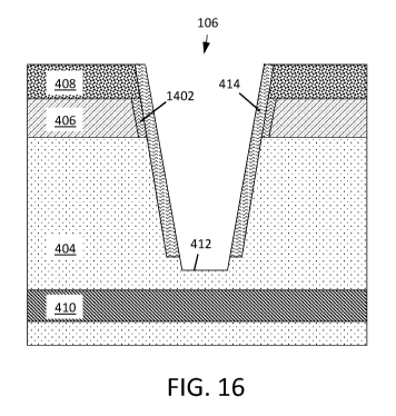
capable of
withstanding corrosive solutions by protecting the underlying material of the
exposed surface,
for example, in bioassays that require the use of corrosive solutions or other
harsh conditions
(e.g., high salt solutions, multiple solution washes, etc.). Surface coatings
can also provide a
more favorable interface for reagents in a bioassay, such as anti-fouling
surface coatings
which reduce or eliminate the adherence of reagent components in a biological
reaction.
Examples of suitable surface coatings and surface modification processes are
described in
U.S. Patent Application 15/971,493, titled "SUBSTRATES HAVING MODIFIED
SURFACE REACTIVITY AND ANTIFOULING PROPERTIES IN BIOLOGICAL
REACTIONS," which is hereby incorporated by reference in its entirety. It
should be
appreciated that such surface coatings may be implemented in the embodiments
of the sample
well described herein.
[0063] FIG. 4 is a cross-sectional view illustrating an exemplary sample
well 106, such
as those shown in the integrated devices of FIG. 1, FIG. 2, FIG. 3A and FIG.
3B. As shown
in FIG. 4, the sample well 106 is defined by an opening formed through a metal
stack 402
17
CA 03109866 2021-02-16
WO 2020/047272 PCT/US2019/048836
disposed on a cladding layer 404 (e.g., SiO2). Metal stack 402 may include one
or more
layers of metal material(s) (e.g., aluminum, titanium, copper). As shown in
FIG. 4, some
embodiments of metal stack 402 include an aluminum layer 406 positioned
proximate to the
top of the cladding layer 404 and a titanium nitride layer 408 over the
aluminum layer 406.
[0064] The aluminum layer 406 may include copper and/or silicon. In some
embodiments, the aluminum layer 406 may include less than approximately 2% of
copper
and/or silicon, and may have a thickness in the range of about 30 nm to 150
nm, or any value
or range of values within that range. In some embodiments, the aluminum layer
is about 65
nm. The titanium nitride layer 408 may include a layer of titanium in contact
with the
aluminum layer 406 and have a thickness of in the range of 1 nm to 150 nm, or
any value or
range of values within that range. In some embodiments, the thickness of
titanium nitride
layer is approximately 80 nm. For illustrative purposes, FIG. 4 also depicts
an exemplary
waveguide structure 410 (e.g., silicon nitride) that facilitates delivery of
excitation optical
energy to the sample well 106.
[0065] The depth, d, of the recess formed in the cladding layer 404 defines
the distance
of light emitted from a label at a bottom surface of sample well 106 to the
aluminum layer
406 (e.g., Al-Cu), which may act as a metal reflector for reflecting light,
such as emission
light. This distance in turn determines the directionality of emission light
toward the optical
sensor (not shown), which may impact optical collection efficiency. Depth, d,
of the recess
may be in the range of 100 nm to 500 nm, or any value or range of values in
that range. In
some embodiments, a depth, d, for the recess is about 300 nm. In some
embodiments, the
depth, d, for the recess is about 360 nm. In addition, the lateral dimensions
(diameter) of the
sample well may impact the ability of a DNA template and dye-labelled
nucleotides to
access, through diffusion, an enzyme that is immobilized at the bottom of the
sample well.
Generally speaking, larger dimensions improve such access. Furthermore, the
lateral
dimensions of the sample well 106 may also impact the volume of the
illumination region
that is illuminated by the waveguide 410. In particular, the dimension wi at
the bottom of the
sample well has a significant impact on the volume of the illumination region
that is excited,
where smaller dimensions result in a smaller volume being excited, which may
in turn
provide a lower background signal. In some embodiments, sample well 106 has a
diameter
WI at the bottom of the recess in the range of 50 nm to 300 nm, or any value
or range of
values in that range. In some embodiments, sample well 106 has a diameter 1422
at the top of
cladding layer 404 in the range of 100 nm to 300 nm, or any value or range of
values in that
range. In some embodiments, sample well 106 has a diameter 1422 at the top of
cladding layer
18
CA 03109866 2021-02-16
WO 2020/047272 PCT/US2019/048836
404 in the range of 150 nm to 250 nm, or any value or range of values in that
range, and a
diameter wi at the bottom of the recess in the range of 75 nm to 200 nm, or
any value or
range of values in that range. In some embodiments, sample well 106 may have
tapered
sidewalls, as shown in FIG. 4.
[0066] In order to facilitate selective chemical functionalization to
immobilize an
enzyme at the bottom of the sample well 106, the bottom surface 412 of the
sample well 106
should have a different composition than other surfaces (e.g., the sidewalls
414 of the sample
well 106 and top surface 416 of the integrated device). As shown in FIG. 4,
bottom surface
412 of the sample well may be the material of the cladding layer (e.g.,
exposed SiO2) and the
sidewalls 414 of the sample well 106 may be a spacer material 418. Spacer
material 418 may
include one or more metal oxides (e.g., TiO2, A1203, 5i02, TiN, Hf02, ZrO2,
and Ta205). The
top surface 416 of the integrated device may include one or more metal oxide
materials
formed by oxidation of the top surface of layer 408 (e.g., TiO2 formed by
oxidation of TiN).
[0067] In some embodiments, it may be desired to have the exposed surfaces
of the
integrated device (top surface, sample well sidewalls, bottom surface) be
substantially stable
for particular types of solutions, including those used during operation of
the integrated
device and during surface functionalization. For example, some solutions that
are used for
device operation may include high ionic strength aqueous solutions, and the
exposed surfaces
of the integrated device may be substantially stable when in contact with such
solutions for a
desired period of time. As another example, some solutions that are used for
surface
functionalization of the integrated device may include acidic solutions, and
the exposed
surfaces of the integrated device may be substantially stable when in contact
with such
solutions for a desired period of time. According to some embodiments where
aluminum is
included in one or more layers of the integrated device, it may be preferable
to have those one
or more layers that include aluminum be encapsulated in a final structure,
which may
improve stability of the surfaces of the integrated device. In addition, it
may be desired to
have the surfaces of the integrated device be sufficiently clean to enable
surface
functionalization.
[0068] FIG. 5 is a flow diagram illustrating exemplary process 500 for
forming a sample
well, according to some embodiments. FIGs. 6-11 show cross-sectional views for
some of
the steps of process 500. For ease of illustration, like elements and
components are denoted
with like reference numbers in the various figures. Process 500 includes act
502 of
depositing an aperture metal stack over one or more layers, such as a cladding
layer and a
waveguide. As shown in FIG. 6, a metal aperture film stack, which includes an
aluminum
19
CA 03109866 2021-02-16
WO 2020/047272 PCT/US2019/048836
layer 406 and titanium nitride layer 408 is formed over cladding layer 404 and
waveguide
410. In some embodiments, prior to forming the metal aperture film stack a top
surface of
cladding layer 404 may be planarized using any suitable planarization process
(e.g., a CMP
process). In some embodiments, aluminum layer 406 may be deposited to have a
thickness
of about 65 nm and titanium nitride layer 408 may include a titanium layer
having a thickness
of about 10 nm of Ti and a titanium nitride layer of about 70.
[0069] Next, process 500 proceeds with act 504, which involves patterning
one or more
holes in a photoresist layer over the metal stack and etching an aperture in
at least the metal
stack. The photoresist layer may facilitate the etching process by defining
the aperture in the
metal stack. Act 504 may also include forming a sample well extending into a
cladding layer
under the metal stack. Further details of the patterning of the photoresist
layer and etching
are shown in FIGs. 7-9. As shown in FIG. 7, a bottom antireflective coating
(BARC) layer
702 may first be formed over the titanium nitride layer 408 and photoresist
layer 704 is
formed over BARC layer 702. A hole 706, corresponding to a location of the
resulting
sample well, is then patterned in the photoresist layer 704. Patterning of
photoresist layer
704 may involve any suitable photolithographic techniques, including
photolithographic
exposure and development of the photoresist layer 704. Hole 706 may have any
suitable size
and shape. In some embodiments, hole 706 may have a circular shape and a
diameter in the
range of 150 nm to 225 nm, or any value or range of values in that range. In
further
preparation for aperture etching, the BARC layer 702 may be selectively
removed using a
plasma etching process, or any suitable technique.
[0070] As shown in FIG. 8, an etch of the metal stack, which includes
layers 406, 408, is
performed to define an aperture 802. The etch process used to define the
aperture 802 shown
in FIG. 8 may be performed by the same process used to remove the BARC layer
702 in FIG.
7, such as for example by a plasma etch process, which may involve using C12
and/or BC13.
The plasma etching process may be followed by an 02 ashing step, water rinse
and/or post-
etch cleaning step. In some embodiments, the plasma etching process may be
isotropic and
result in undercut regions in one or more layers of metal stack. For example,
a Cl-based etch
of aluminum may be somewhat isotropic in nature, which may lead to undercut
regions 804
in aluminum layer 406. In some embodiments, a wet clean step can contribute to
the
formation undercut regions in metal stack, such as undercut regions 804.
[0071] FIG. 9 shows sample well 902, having sidewalls 904, formed by an
etch of
cladding layer 404. Oxide material of the cladding layer 404 may be removed
through the
use of a dry fluorocarbon etch (e.g., CF4, CHF3, C4F8, C3H2F6), followed by an
02 ashing step
CA 03109866 2021-02-16
WO 2020/047272 PCT/US2019/048836
and post-etch cleaning step. In some embodiments, the dry etching process may
occur for a
duration of time to achieve a desired etch depth or, alternatively through the
use of an etch
stop layer (not shown) positioned at a location within the cladding layer 404
to achieve the
desired etch depth. In some embodiments one or more sidewalls 904 of the
resulting sample
well 902 formed by the etching process may be at an angle normal to a top
surface of the
integrated device, such as shown in FIG. 9. Sidewalls 904 of the sample well
902 may be
tapered at an angle in the range of 1 to 15 , with respect to a normal to the
top surface of the
integrated device. In other words, the sample well 902 may be tapered such
that its diameter
decreases with increasing depth.
[0072] Returning to FIG. 7, the photoresist layer 704 and/or BARC layer 702
may be
removed from the metal stack 406, 408 using a plasma removal process (e.g.,
ashing,
cleaning), or any suitable technique. In some embodiments, the photoresist
layer 704 and/or
BARC layer 702 are removed after etching of metal stack 406, 408 (which is
shown in FIG.
8) and prior to etching of the cladding layer 404 (which is shown in FIG. 9).
In some
embodiments, the photoresist layer 704 and/or BARC layer 702 are removed after
etching of
both metal stack 406, 408 and top cladding the cladding layer 404.
[0073] Process 500 proceeds by act 506, which includes depositing spacer
material on
the sidewall(s) of the sample well. The space material may be deposited in a
conformal
manner, and may be referred to as "a conformal spacer layer" in some
embodiments. As
shown in FIG. 10, spacer layer 1002 is deposited in sample well 902, and may
contact one or
more of cladding layer 404 and metal stack, including layers 406 and 408.
Examples of
spacer materials that may be used as a spacer layer may include A1203, TiN,
Ta205, TaN,
ZrO2, TiO2, and Hf02. A thickness of the spacer layer may be in the range of 3
nm to 50 nm,
or any value or range of values in that range. In some embodiments, spacer
layer 1002 may
be a layer of TiO2 having a thickness between about 3 nm to about 30 nm. In
some
embodiments, spacer layer 1002 may be a layer of TiO2 formed by atomic layer
deposition
(ALD) at a temperature of about 230 C and has a thickness of about 12 nm. In
some
embodiments, conformal spacer layer 1002 may include multiple layers of
materials. In such
embodiments, the multiple layers of materials may facilitate fabrication,
surface
functionalization, and/or surface cleaning.
[0074] Then, process 500 proceeds by act 508, which includes etching the
spacer
material. In some embodiments, an anisotropic (directional) etch may be used
in etching the
spacer material and remove horizontally disposed surfaces of the spacer layer,
which may
result in the spacer material along vertical surfaces, such as the sidewalls
of a sample well.
21
CA 03109866 2021-02-16
WO 2020/047272 PCT/US2019/048836
As shown in FIG. 11, an anisotropic etch of spacer layer 1002 removed the
horizontal
surfaces at the bottom of the sample well and the top surface of the
integrated device, such
that sidewall spacers 414 are formed in the resulting sample well 106. In
addition, bottom
surface 412 of sample well 106 is exposed cladding material (e.g., Si02). In
embodiments
where the spacer layer includes Ti02, and results in sidewall spacers having
Ti02, a
fluorocarbon or BC13 etch chemistry (with 02 and/or air) may be used. In
embodiments
where the spacer layer includes A1203, and results in sidewall spacers having
A1203, a BC13
etch chemistry (with C12 and/or air) may be used. As the bottom surface 412 of
the sample
well 106 is of a different material than the sidewall spacers 414 and top
surface of the
integrated device, the resulting structure may provide a different
functionality for preferential
binding of a sample (not shown) to the bottom surface 412 in comparison to the
sidewalls 414
of the sample well. Thus, upon completion of the sample well structure etch,
additional
processing steps may be performed such as, for example, attachment of biotin
species on the
bottom surface 412 of the sample well 106 and chip passivation. Examples of
additional
processing steps that result in modified bottom surface chemistry and
passivation are
described in U.S. Patent Application 15/971,493, which is hereby incorporated
by reference
in its entirety.
[0075] Possible side effects of process 500 described above may be the
presence of
aluminum fluoride (AlF) and other residues on the aperture and sample well
sidewalls from a
fluorocarbon based etch. Such residues in turn may affect the integrity of the
sidewall spacer
deposition. In addition, the exposed aluminum of layer 406 may also be subject
to other
deleterious effects, such as from corrosion or humidity. In addition, for
embodiments where
the top titanium nitride layer 408 serves as an etch mask for removing the
cladding material,
it is further possible that edges of the top titanium nitride layer 408
adjacent the aperture
(such as aperture 802 shown in FIG. 8) could become eroded during the sample
well etch
processing and result in exposed aluminum.
[0076] Some embodiments may involve using an encapsulant spacer to protect
sidewalls
of the aperture metal stack, such as an aluminum layer in the metal stack.
FIG. 12 is a flow
diagram illustrating exemplary process 1200 for forming a sample well
structure. FIGs. 13-
16 show cross-sectional views for some of the steps of process 1200. As shown
in FIG. 12,
the process 1200 begins at act 1202 by depositing a metal stack over one or
more layers, such
as a cladding layer or a waveguide. Depositing the metal stack may be
performed using
processes and materials described above in connection with process 500.
Process 1200
proceeds to act 1204, which includes etching an aperture into the metal stack
by patterning a
22
CA 03109866 2021-02-16
WO 2020/047272 PCT/US2019/048836
photoresist material and, in some embodiments, a BARC layer. Etching the
aperture into the
metal stack may be performed using processes and materials described above in
connection
with process 500, and shown in FIG. 7 and FIG. 8. FIG. 13 shows etched metal
stack 406,
408 over cladding layer 404.
[0077] In contrast to the process 500, process 1200 proceeds to act 1206,
which involves
depositing an encapsulant spacer material within the aperture formed by act
1204. FIG. 13
shows encapsulant spacer material 1302 formed within aperture 802, contacting
a surface of
cladding layer 404, metal stack 406, 408, and top surface. Encapsulant spacer
material 1302
may be any suitable material that acts to protect one or more layers of metal
stack 406, 408
during subsequent processing steps, and in particular, may reduce or prevent
the formation of
metal fluoride residue from subsequent etching of the cladding material 404.
The
encapsulant spacer material 1302 may include one or more silicon materials.
Examples of
suitable materials in encapsulant spacer material 1302 may include amorphous
silicon (a-Si),
SiO2, SiON, SiN, and one or more silicon alloys (e.g., silicon-rich oxide
(SRO), silicon-rich
nitride (SRN)). In some embodiments, the encapsulant spacer material 1302 may
be
amorphous silicon (a-Si) deposited by plasma enhanced chemical vapor
deposition
(PECVD). In other embodiments, the encapsulant spacer material 1302 may be
PECVD
deposited SiO2, SiON, or SiN. In some embodiments, the encapsulant spacer
material 1302
may be an oxide material (e.g., TiO2, A1203, SiO2, Hf02, TiN, Ta205, ZrO2)
formed by
atomic layer deposition (ALD). In some embodiments, encapsulant spacer
material 1302
may include multiple layers of one or more materials. Generally, the
encapsulant spacer
material 1302 may be deposited in a conformal manner with respect to the top
surface of
metal layer 408 and the bottom of the aperture 802. In some embodiments, the
encapsulant
spacer material 1302 may have varying thickness. For example, encapsulant
spacer material
1302 may have a larger thickness at locations on the top surface of metal
layer 408 than along
the bottom of the aperture 802.
[0078] Process 1200 continues by act 1208, where the encapsulant spacer
material is
etched and the cladding material is etched to form a sample well. FIG. 14
shows sample well
902 formed by etching encapsulant spacer material and cladding layer 404. In
some
embodiments, the encapsulant spacer etch and/or the sample well etch may
involve a
fluorocarbon based etch, such as described above, followed by an 02 ash
process and a post-
etch clean process. In embodiments where the etch of the encapsulant material
and cladding
material is substantially an anisotropic, directional etch, one or more
portions of the
encapsulant spacer material may remain on sidewalls of the metal stack. As
shown in
23
CA 03109866 2021-02-16
WO 2020/047272 PCT/US2019/048836
FIG. 14, the aluminum layer 406 has one or more undercut regions where
encapsulant spacer
1402 remains after the etching to form the sample well. The encapsulant spacer
1402 may
advantageously protect the exposed aluminum sidewalls of layer 406. Protection
by the
encapsulant spacer 1402 may reduce or prevent formation of metal fluoride
residues during
the sample well etch, which might otherwise be vulnerable to
corrosion/humidity or reaction
with F, Cl during subsequent etching.
[0079] From this point, process 1200 may continue similar to that of
process 500.
Process 1200 may proceed with act 1210, where a sidewall spacer material is
deposited,
which may involve using similar materials and processes as described in
connection with act
506 of process 500. FIG. 15 shows sidewall spacer material 1002, which
contacts
encapsulant spacer portions 1402. Examples of spacer materials that may be
used to form
sidewall spacer material 1002 include A1203, Ti02, TiN, Ta205, TaN, Zr02 and
Hf02. In
some embodiments, the sidewall spacer material 1002 may include multiple
layers of one or
more materials. In some embodiments, the sidewall spacer material 1002 may be
a layer of
TiO2 formed to a thickness between about 3 nm to about 30 nm. In some
embodiments, the
sidewall spacer material 1002 may be a layer of TiO2 formed to a thickness of
about 12 nm
by atomic layer deposition (ALD) at a temperature of about 230 C.
[0080] Process 1200 proceeds to act 1212, where the sidewall spacer
material is etched
to form the resulting sample well, which may involve using similar materials
and processes
as described in connection with act 508 of process 500. As shown in FIG. 16,
an anisotropic
etch of spacer layer 1002 removed the horizontal surfaces at the bottom of the
sample well
and the top surface of the integrated device, such that sidewall spacers 1402
are formed in the
resulting sample well 106. In addition, bottom surface 412 of sample well 106
is exposed
cladding material (e.g., Si02). In embodiments where the spacer layer includes
Ti02, and
results in sidewall spacers having Ti02, a fluorocarbon or BC13 etch chemistry
(with 02
and/or air) may be used. In embodiments where the spacer layer includes A1203,
and results
in sidewall spacers having A1203, a BC13 etch chemistry (with C12 and/or air)
may be used.
[0081] Some embodiments involve using a dielectric etch mask, formed over
the
aperture metal stack, which may protect the top surface of the metal stack
during subsequent
etching, such as the aperture etch and the sample well etch. The dielectric
etch mask may be
gradually removed throughout the steps in fabricating the sample well, and in
some
embodiments may be substantially cleared in the resulting sample well
structure. Depending
on the type of dielectric material used in the dielectric etch mask, the
dielectric etch mask
may provide a strong endpoint signal for process control in etching the sample
well. The
24
CA 03109866 2021-02-16
WO 2020/047272 PCT/US2019/048836
thickness of the top layer depends on the etch selectivity of the dielectric
relative to the
cladding layer, and the amount of over-etch desired.
[0082] FIG. 17 is a flow diagram illustrating exemplary process 1700 for
forming a
sample well structure. FIGs. 18-25 show cross-sectional views for some of the
steps of
process 1700. As shown in FIG. 17, the process 1700 begins at act 1702 by
depositing a
metal stack over one or more layers, such as a cladding layer or a waveguide.
Depositing the
metal stack may be performed using processes and materials described above in
connection
with process 500. In some embodiments, metal stack may include aluminum layer
406 and
titanium nitride layer 408 over cladding layer 404 and waveguide 410, as shown
in FIG. 18.
Act 1702 may further include depositing a dielectric layer over the metal
stack. As shown in
FIG. 18, dielectric layer 1802 is formed over metal stack, which includes
layers 406 and 408.
The dielectric layer 1802 may include one or more silicon materials. Examples
of suitable
materials that may be included in dielectric layer 1802 include amorphous
silicon (a-Si),
SiO2, SiON, SiN, and silicon alloy (e.g., silicon-rich oxide (SRO) and silicon-
rich nitride
(SRN)). Dielectric layer 1802 may have a thickness in the range of 30 to 400
nm, or any
value or range of values in that range. In some embodiments, dielectric layer
1802 may be
PECVD SiO2, deposited at a thickness of about 150-300 nm. In some embodiments,
dielectric layer 1802 may be PECVD SiN, deposited at a thickness of about 50-
300 nm. In
some embodiments, dielectric layer 1802 may be PECVD SiON, deposited at a
thickness of
about 50-300nm.
[0083] Process 1700 may proceed to act 1704, where a photoresist material
is patterned
to define aperture openings, and etching an aperture and sample well. The
pattern is then
etched into the dielectric mask, aperture metal stack, and ultimately the
cladding layer to
form the sample well. In some embodiments, the photoresist material may be
deposited over
a BARC layer. In some embodiments, patterned opening may be a circular opening
having a
diameter in the range of about 150 to 225 nm diameter. Etching the aperture
into the metal
stack may be performed using processes and materials described above in
connection with
process 500, and shown in FIG. 7 and FIG. 8. FIG. 19 illustrates a point in
the processing
following etching of the dielectric layer 1802 and removal of the photoresist
material (not
shown). With the dielectric layer 1802 patterned as a hardmask, the aperture
in metal stack
406, 408 may then be etched as shown in FIG. 20, which shows aperture 802 and
undercut
regions 804. Etching the aperture into the metal stack may be performed using
processes and
materials described above in connection with process 500, and shown in FIG. 7
and FIG. 8.
In some embodiments, etching of the aperture in the metal stack may involve a
plasma etch
CA 03109866 2021-02-16
WO 2020/047272 PCT/US2019/048836
process, such as a plasma etch process that includes C12 and/or BC13. The
plasma metal
etching process may be followed by water rinse and/or post-etch cleaning step.
At this point,
the structure is prepared for the sample well etch into the cladding layer,
such as cladding
layer 404.
[0084] In some embodiments, the dielectric layer 1802 is selected from a
material having
the same or similar etch characteristics with respect to the cladding layer
404. In such
embodiments, the dielectric layer 1802 may be removed as the sample well 902
is etched. An
intermediate point in the sample well etch processing is illustrated in FIG.
21, which shows a
portion of the dielectric layer 1802 remaining as sample well 902 is at an
intermediate stage
of being formed. In particular, as compared to FIG. 20, it will be seen from
FIG. 21 that the
dielectric layer 1802, while still protecting the aperture metal stack 406,
408 from the etching
process (e.g., a fluorocarbon based etch), has been reduced in thickness by
roughly an amount
corresponding to the present etch depth of the sample well 902 being formed.
FIG. 22
illustrates a later point in time during the sample well etch process, where
the dielectric layer
1802 is mostly consumed and the sample well 902 is mostly etched. Eventually,
as shown in
FIG. 23, the dielectric layer 1802 is removed as the sample well etch is at or
near completion.
In particular, the thickness of the dielectric etch mask depend on the etch
rate of the dielectric
etch mask material during the etch of the sample well, such that the material
of the dielectric
etch mask is substantially or completely removed at or near the end of the
etching of the
sample well. In embodiments where the dielectric layer 1802 is SiO2, the
dielectric layer
1802 may provide a strong endpoint signal for process control in etching the
sample well
since the TiN metal layer 408 is exposed once the dielectric etch mask is
substantially or
completely removed. In such embodiments where SiO2 is used as the dielectric
mask
material, the thickness of the dielectric layer may correspond to the desired
depth of the
sample well (e.g., may be slightly less than the desired depth of the sample
well) so that the
mask is substantially or fully removed when the sample well is etched to the
correct depth.
[0085] From this point, process 1700 may continue similar to that of
process 500.
Process 1700 may proceed with act 1706, where a sidewall spacer material is
deposited,
which may involve using similar materials and processes as described in
connection with act
506 of process 500. FIG. 24 shows sidewall spacer material 1002, which
contacts both layers
406 and 408. As shown in FIG. 24, undercut regions may form in layer 406 and
sidewall
spacer material 1002 may fill the undercut regions. Examples of spacer
materials that may be
used to form sidewall spacer material 1002 include A1203, TiO2, TiN, Ta205,
TaN, ZrO2 and
Hf02. In some embodiments, the sidewall spacer material 1002 may be a layer of
TiO2
26
CA 03109866 2021-02-16
WO 2020/047272 PCT/US2019/048836
formed to a thickness between about 3 nm to about 30 nm. In some embodiments,
the
sidewall spacer material 1002 may be a layer of TiO2 formed to a thickness of
about 12 nm
by atomic layer deposition (ALD) at a temperature of about 230 C.
[0086] Process 1700 proceeds to act 1708, where the sidewall spacer
material is etched
to form the resulting sample well, which may involve using similar materials
and processes
as described in connection with act 508 of process 500. As shown in FIG. 25,
an anisotropic
etch of spacer layer 1002 removed the horizontal surfaces at the bottom of the
sample well
and the top surface of the integrated device, such that sidewall spacers 414
are formed in the
resulting sample well 106. In addition, bottom surface 412 of sample well 106
is exposed
cladding material (e.g., Si02). In embodiments where the spacer layer includes
Ti02, and
results in sidewall spacers having Ti02, a fluorocarbon or BC13 etch chemistry
(with 02
and/or air) may be used. In embodiments where the spacer layer includes A1203,
and results
in sidewall spacers having A1203, a BC13 etch chemistry (with C12 and/or air)
may be used.
[0087] The above-described embodiments can be implemented in any of
numerous ways.
For example, the embodiments may be implemented using hardware, software or a
combination thereof. When implemented in software, the software code can be
executed on
any suitable processor (e.g., a microprocessor) or collection of processors,
whether provided
in a single computing device or distributed among multiple computing devices.
It should be
appreciated that any component or collection of components that perform the
functions
described above can be generically considered as one or more controllers that
control the
above-discussed functions. The one or more controllers can be implemented in
numerous
ways, such as with dedicated hardware, or with general purpose hardware (e.g.,
one or more
processors) that is programmed using microcode or software to perform the
functions recited
above.
[0088] The described embodiments can be implemented in various
combinations.
Example configurations include methods (1) ¨ (33), and integrated devices (34)-
(43) below.
[0089] (1) A method of forming an integrated device, the method comprising:
forming a
metal stack over a cladding layer; forming an aperture in the metal stack;
forming first spacer
material within the aperture; and forming a sample well by removing some of
the cladding
layer to extend a depth of the aperture into the cladding layer, wherein at
least one portion of
the first spacer material is in contact with at least one layer of the metal
stack.
[0090] (2) The method of (1), wherein forming the metal stack further
comprises
forming the metal stack on the cladding layer.
[0091] (3) The method of (1) or (2), wherein forming the first spacer
material further
27
CA 03109866 2021-02-16
WO 2020/047272 PCT/US2019/048836
comprises forming the first spacer material over the metal stack and at a
bottom surface of the
aperture.
[0092] (4) The method of any one of (1)-(3), wherein forming the sample
well further
comprises performing a first directional etch to remove at least some of the
first spacer
material disposed on a top surface of the metal stack and on a bottom surface
of the aperture.
[0093] (5) The method of any one of (1)-(4), wherein the first spacer
material includes at
least one material configured to reduce formation of metal fluoride residue
during an etch
process used in forming the sample well.
[0094] (6) The method of any one of (1)-(5), wherein the first spacer
material includes at
least one material configured to reduce formation of metal fluoride residue on
at least one
metal layer of the metal stack during an etch process used in forming the
sample well.
[0095] (7) The method of any one of (1)-(6), wherein the at least one
portion of the first
spacer material is disposed at an undercut region of the metal stack.
[0096] (8) The method of any one of (1)-(7), wherein the metal stack
comprises at least
one aluminum containing layer and at least one titanium containing layer.
[0097] (9) The method of any one of (1)-(8), wherein the first spacer
material is formed
by plasma enhanced chemical vapor deposition (PECVD).
[0098] (10) The method of any one of (1)-(9), wherein the first spacer
material includes
at least one silicon material.
[0099] (11) The method of any one of (1)-(10), wherein the first spacer
material
comprises one or more layers selected from the group of: amorphous silicon (a-
Si), SiO2,
SiON, SiN, and silicon alloy.
[00100] (12) The method of any one of (1)-(11), wherein the first spacer
material is
formed by atomic layer deposition (ALD).
[00101] (13) The method of any one of (1)-(12), wherein the first spacer
material
comprises one or more layers selected from the group of: TiO2, A1203, SiO2,
Hf02, TiN,
Ta205, and ZrO2.
[00102] (14) The method of any one of (1)-(13), wherein the cladding layer
comprises
SiO2.
[00103] (15) The method of any one of (1)-(14), further comprising: forming
second
spacer material into the sample well; and removing at least some of the second
spacer
material at a bottom surface of the sample well to expose a portion of the
cladding layer,
wherein at least one portion of the second spacer material is in contact with
one or more of
the metal stack, the at least one portion of the first spacer material, and
the cladding later.
28
CA 03109866 2021-02-16
WO 2020/047272 PCT/US2019/048836
[00104] (16) The method of (15), wherein forming the second spacer material
further
comprises forming the second spacer material over the metal stack.
[00105] (17) The method of (15) or (16), wherein removing the at least some
of the
second spacer material further comprises performing a directional etch to
remove second
spacer material disposed on a top surface of the metal stack and on the bottom
surface of the
sample well.
[00106] (18) The method of (17), wherein the directional etch comprises a
fluorocarbon
based etch.
[00107] (19) The method of any one of (15)-(18), wherein the second spacer
material is
formed by atomic layer deposition (ALD).
[00108] (20) The method of any one of (15)-(19), wherein the second spacer
material
comprises one or more layers selected from the group of: TiO2, A1203, Hf02,
ZrO2, and
Ta205.
[00109] (21) A method of forming an integrated device, the method
comprising: forming
a metal stack over a cladding layer; forming a dielectric layer over the metal
stack; forming
an aperture in the metal stack by forming an opening in the dielectric layer
and using the
dielectric layer as a mask in removing a portion of the metal stack; and
forming a sample well
by removing a portion of the cladding layer, wherein at least a portion of
dielectric layer is
removed while forming the sample well.
[00110] (22) The method of (21), wherein forming the metal stack further
comprises
forming the metal stack on the cladding layer.
[00111] (23) The method of (21) or (22), wherein forming the dielectric
material further
comprises forming the dielectric layer on the metal stack.
[00112] (24) The method of any one of (21)-(23), wherein forming the
aperture further
comprises etching the opening in the dielectric layer and using the dielectric
layer as an etch
mask to form the aperture in the metal stack.
[00113] (25) The method of any one of (21)-(24), wherein forming the sample
well further
comprises etching the cladding layer and the dielectric layer simultaneously.
[00114] (26) The method of any one of (21)-(25), wherein the metal stack
comprises at
least one aluminum containing layer and at least one titanium containing
layer.
[00115] (27) The method of any one of (21)-(26), wherein the cladding layer
comprises
SiO2.
[00116] (28) The method of any one of (21)-(27), further comprising:
forming a spacer
layer over the metal stack and into the sample well; and performing a
directional etch to
29
CA 03109866 2021-02-16
WO 2020/047272 PCT/US2019/048836
remove portions of the spacer layer disposed on a top surface of the metal
stack and on a
bottom surface of the sample well to expose a portion of the cladding layer;
wherein at least
one portion of the spacer layer forms at least one sidewall of the sample
well.
[00117] (29) The method of (28), wherein the spacer layer is formed by
atomic layer
deposition (ALD).
[00118] (30) The method of (28) or (29), wherein the spacer layer comprises
one or more
layers selected from the group of: TiO2, A1203, Hf02, ZrO2, and Ta205.
[00119] (31) The method of any one of (21)-(30), wherein forming the sample
well further
comprises substantially removing the dielectric layer.
[00120] (32) The method of any one of (21)-(31), wherein the integrated
device after
forming the sample well does not include the dielectric layer.
[00121] (33) The method of any one of (21)-(32), wherein the dielectric
layer comprises
one or more selected from the group of: amorphous silicon (a-Si), SiO2, SiON,
SiN, and
silicon alloy.
[00122] (34) An integrated device comprising: a cladding layer; a metal
stack formed over
the cladding layer and having at least one undercut region; a sample well
extending through
the metal stack proximate to the at least one undercut region and into the
cladding layer; and
a first spacer material filling the at least one undercut region.
[00123] (35) The integrated device of configuration (34), wherein the first
spacer material
forms at least one sidewall of the sample well.
[00124] (36) The integrated device of configuration (34) or (35), wherein
the first spacer
material comprises one or more selected from the group of: amorphous silicon
(a-Si), SiO2,
SiON, and SiN.
[00125] (37) The integrated device of any one of configurations (34)-(36),
wherein the
first spacer material comprises one or more selected from the group of: TiO2,
A1203, Hf02,
TiN, ZrO2, and Ta205.
[00126] (38) The integrated device of any one of configurations (34)-(37),
wherein the
metal stack comprises at least one layer including aluminum and at least one
layer including
titanium.
[00127] (39) The integrated device of any one of configurations (34)-(38),
wherein the
cladding layer comprises SiO2.
[00128] (40) The integrated device of any one of configurations (34)-(39),
further
comprising a second spacer material in contact with one or more of the metal
stack, the first
spacer material, and the cladding layer.
CA 03109866 2021-02-16
WO 2020/047272 PCT/US2019/048836
[00129] (41) The integrated device of configuration (40), wherein the
second spacer
material forms at least one sidewall of the sample well.
[00130] (42) The integrated device of configuration (40) or (41), wherein
the second
spacer material comprises one or more layers selected from the group of: TiO2,
A1203, Hf02,
ZrO2, and Ta205.
[00131] (43) The integrated device of any one of configurations (34)-(42),
wherein the
metal stack comprises a first layer formed over a second layer, and the
undercut region is
formed in the second layer.
[00132] Having thus described several aspects and embodiments of the
technology of this
application, it is to be appreciated that various alterations, modifications,
and improvements
will readily occur to those of ordinary skill in the art. Such alterations,
modifications, and
improvements are intended to be within the spirit and scope of the technology
described in
the application. It is, therefore, to be understood that the foregoing
embodiments are
presented by way of example only and that, within the scope of the appended
claims and
equivalents thereto, inventive embodiments may be practiced otherwise than as
specifically
described. In addition, any combination of two or more features, systems,
articles, materials,
kits, and/or methods described herein, if such features, systems, articles,
materials, kits,
and/or methods are not mutually inconsistent, is included within the scope of
the present
disclosure.
[00133] Also, as described, some aspects may be embodied as one or more
methods. The
acts performed as part of the method may be ordered in any suitable way.
Accordingly,
embodiments may be constructed in which acts are performed in an order
different than
illustrated, which may include performing some acts simultaneously, even
though shown as
sequential acts in illustrative embodiments.
[00134] All definitions, as defined and used herein, should be understood
to control over
dictionary definitions, definitions in documents incorporated by reference,
and/or ordinary
meanings of the defined terms.
[00135] The indefinite articles "a" and "an," as used herein in the
specification and in the
claims, unless clearly indicated to the contrary, should be understood to mean
"at least one."
[00136] The phrase "and/or," as used herein in the specification and in the
claims, should
be understood to mean "either or both" of the elements so conjoined, i.e.,
elements that are
conjunctively present in some cases and disjunctively present in other cases.
[00137] As used herein in the specification and in the claims, the phrase
"at least one," in
reference to a list of one or more elements, should be understood to mean at
least one element
31
CA 03109866 2021-02-16
WO 2020/047272 PCT/US2019/048836
selected from any one or more of the elements in the list of elements, but not
necessarily
including at least one of each and every element specifically listed within
the list of elements
and not excluding any combinations of elements in the list of elements. This
definition also
allows that elements may optionally be present other than the elements
specifically identified
within the list of elements to which the phrase "at least one" refers, whether
related or
unrelated to those elements specifically identified.
[00138] Use of ordinal terms such as "first," "second," "third," etc., in
the claims to
modify a claim element does not by itself connote any priority, precedence, or
order of one
claim element over another or the temporal order in which acts of a method are
performed,
but are used merely as labels to distinguish one claim element having a
certain name from
another element having a same name (but for use of the ordinal term) to
distinguish the claim
elements.
[00139] In the claims, as well as in the specification above, all
transitional phrases such as
"comprising," "including," "carrying," "having," "containing," "involving,"
"holding,"
"composed of," and the like are to be understood to be open-ended, i.e., to
mean including
but not limited to. The transitional phrases "consisting of' and "consisting
essentially of'
shall be closed or semi-closed transitional phrases, respectively.
32