Note: Descriptions are shown in the official language in which they were submitted.
CA 03111645 2021-03-04
SYNCHRONIZATION SIGNAL TRANSMISSION METHOD,
TRANSMITTING END DEVICE AND RECEIVING END DEVICE
Technical field
The embodiments of this application relate to the field of communication, and
in paticular,
to a method of synchronous signal transmission, a transmitting device and a
receiving end
device.
Related Art
In 5-Generation New Radio (5G NR) system, in order to meet the flexibility of
network
deployment, it is necessary to ensure that cell synchronization signals can be
deployed in any
available frequency band to assist cell establishment. Driven by the above
requirements, the
synchronization raster (SS raster) in 5G NR system are relatively dense in
order to provide
enough frequency position for base stations to establish cells and UE to
access the cells.
When communicating on the unlicensed frequency band, the initial access
bandwidth of
the cell in the unlicensed frequency band is not more than 20MHz, and the
candidate positions
of each 20MHz bandwidth on the unlicensed frequency band are also constrained.
Therefore,
the deployment of the initial access sub-band position of the cell in the
unlicensed frequency
band must be limited. It is obviously inefficient to continue to use the dense
SS raster defined
by 5G NR as the position of synchronization signals for terminal devices to
retrieve.
Therefore, how to design SS raster with unlicensed frequency band is an urgent
problem to be
solved.
SUMMARY
The embodiments of this application provide a synchronous signal transmission
method,
a transmitting device and a receiving end device, and designs frequency domain
candidate
positions of a synchronous signal on an unlicensed frequency band (also called
SS raster),
which can reduce the complexity of cell initially searching and reduce the
influence of the
position, where a cell in the unlicensed frequency band initially access the
SS/PBCH block
(SSB) in the subband, on the other channels in the subband.
In the first aspect, a method of synchronous signal transmission is provided,
which
includes:
1
Date Recue/Date Received 2021-03-04
CA 03111645 2021-03-04
The transmitting device transmits a synchronization signal block on a first
frequency
domain position, the first frequency domain position is located on the
frequency domain
candidate position of the synchronization signal, and each 20 MHz subband
includes at least
one frequency domain candidate position of the synchronization signal.
Optionally, the first frequency domain position may be a resource on an
unlicensed
spectrum.
It should be noted that the transmitting device may be a network device.
In the second aspect, a method of synchronous signal transmission is provided,
which
includes:
the receiving device monitors for the synchronization signal block on a first
frequency
domain position, a first frequency domain position is located on the frequency
domain
candidate position of the synchronization signal, and each 20 MHz subband
includes at least
one frequency domain candidate position of the synchronization signal.
It should be noted that the receiving device may be a terminal device.
In the third aspect, a transmitting device is provided for performing the
methods in the
first aspect or the embodiments thereof.
Specifically, the transmitting device includes a functional module for
performing the
methods in the first aspect described above or the embodiments thereof.
In the fourth aspect, a receiving device is provided for performing the method
in the
second aspect described above or the embodiments thereof.
Specifically, the receiving device includes a functional module for performing
the
methods in the second aspect or the embodiments thereof.
In the fifth aspect, a transmitting device is provided, including a processor
and a memory.
The memory is used to a store computer program, and the processor is used to
call and run the
computer program stored in the memory to execute the methods in the first
aspect or the
embodiments thereof.
In the sixth aspect, a receiving device is provided, including a processor and
a memory.
The memory is used to store a computer program, and the processor is used to
call and run the
computer program stored in the memory to execute the methods in the second
aspect or the
embodiments thereof.
In the seventh aspect, a chip is provided to execute the methods in any aspect
of the first
and the second aspects or the embodiments thereof.
2
Date Recue/Date Received 2021-03-04
CA 03111645 2021-03-04
Specifically, the chip includes a processor for calling and running a computer
program
from a memory so that the device installed with the chip performs the methods
in any aspect
of the first and the second aspects or the embodiments thereof.
In the eighth aspect, a computer-readable storage medium is provided for
storing a
computer program that causes the computer to perform the methods in any aspect
of the first
and the second aspects or the embodiments thereof.
In the ninth aspect, a computer program product is provided, including a
computer
program instruction that causes the computer to perform the methods in any
aspect of the first
and the second aspects or the embodiments thereof.
In the tenth aspect, a computer program is provided, when which is running on
a
computer, causes the computer to perform the methods in any aspect of the
first and the
second aspects or the embodiments thereof.
The above embodiments design the frequency domain candidate position of
synchronization signal on the unlicensed frequency band (also called SS
raster), which can
reduce the complexity of cell initially searching and reduce the influence of
the position,
where a cell in the unlicensed frequency band initially access the SS/PBCH
block (SSB) in
the subband, on the other channels in the subband.
BRIEF DESRIPTION OF THE DRAWINGS
Fig.1 is a schematic diagram of a communication system architecture according
to the
embodiment of this application.
Fig.2 is a schematic flow chart of a synchronous signal transmission method
according to
the embodiment of this application.
Fig.3 is another schematic diagram of a synchronous signal transmission
according to an
embodiment of this application.
Fig.4 is another schematic diagram of another synchronous signal transmission
according
to an embodiment of this application.
Fig.5 is another schematic diagram of another synchronous signal transmission
according
to an embodiment of this application.
Fig.6 is another schematic diagram of another synchronous signal transmission
according
to an embodiment of this application.
Fig.7 is another schematic diagram of another synchronous signal transmission
according
to the embodiment of this application.
3
Date Recue/Date Received 2021-03-04
CA 03111645 2021-03-04
Fig.8 is another schematic diagram of another synchronous signal transmission
according
to an embodiment of this application.
Fig.9 is another schematic diagram of another synchronous signal transmission
according
to an embodiment of this application.
Fig.10 is a schematic flow chart of another synchronous signal transmission
method
according to the embodiment of this application.
Fig.11 is a schematic block diagram of a transmitting device according to an
embodiment
of this application.
Fig.12 is a schematic block diagram of a receiving device according to an
embodiment of
this application.
Fig.13 is a schematic block diagram of a communication device according to an
embodiment of this application.
Fig.14 is a schematic block diagram of a chip according to an embodiment of
this
application.
Fig.15 is a schematic block diagram of a communication system according to an
embodiment of this application.
DETAILED DESCRIPTION
The following describes the technical solutions in the embodiments of this
application
with reference to the the drawings in the embodiments of this application.
Obviously, the
described embodiments are some of the embodiments of this application rather
than all the
embodiments. Based on the embodiments of this application, all other
embodiments obtained
by a person of ordinary skill in the art without creative efforts shall fall
within the protection
scope of this application.
The embodiment of this application can be applied to various communication
systems,
such as global system of mobile communication (GSM), a code division multiple
access
(CDMA) system, a wideband code division multiple access (WCDMA) system and a
general
packet radio service (GPRS), a long term evolution (LTE) system, an advanced
long term
evolution (LTE-A) system, a new radio (NR) system, a NR system evolution
system, LTE
system on unlicensed spectrum(LTE-U), a NR based access to unlicensed
spectrum) system
on unlicensed spectrum (NR-U) system, a universal mobile communication system
(UMTS),
a wireless local area networks (WLAN), a wireless fidelity (WiFi), a next
generation
communication system or other communication systems.
4
Date Recue/Date Received 2021-03-04
CA 03111645 2021-03-04
Generally speaking, the traditional communication system supports a limited
number of
connections and is easy to implement. However, with the development of
communication
technology, mobile communication system will not only support traditional
communications,
but also support, for example, device to device (D2D) communication, machine
to machine
(M2M) communication, machine type communication (MTC), and vehicle to vehicle
(V2V)
communication and so on. The embodiments of this application can also be
applied to these
communication systems.
Optionally, the communication systems in the embodiments of this application
can be
applied to the carrier aggregation (CA) scenario, the dual connectivity (DC)
scenario, and the
.. stand-alone (SA) networking scenario.
The embodiments of this application can be applied to unlicensed spectrum.
For example, the communication system 100 applied by the embodiment of this
application is shown in Fig.l. The communication system 100 may include a
network device
110, which may be a device communicating with a terminal device 120 (or called
a
communication terminal or a terminal). The network device 110 may provide
communication
coverage for a specific geographical region and may communicate with the
terminal devices
located in the coverage region.
Fig.1 illustrates an exemplary network device and two terminal devices.
Optionally, the
communication system 100 may include a plurality of network devices, and other
number of
terminal devices may be included within the coverage range of each network
device, which is
not limited in the embodiments of this application.
Optionally, the communication system 100 may further include a network
controller, a
mobility management entity and other network entities, which is not limited in
the
embodiments of this application.
It should be understood that the device with communication function in the
network
system in the embodiments of this application can be called communication
device. Taking
the communication system 100 shown in Fig.1 as an example, the communication
device can
include the network device 110 and the terminal device 120 with the
communication function.
The network device 110 and the terminal device 120 may be the specific device
described
above, which will not be repeated here. The communication device may also
include other
devices in the communication system 100, such as a network controller, a
mobile
management entity and other network entities, which are not limited in the
embodiments of
this application.
5
Date Recue/Date Received 2021-03-04
CA 03111645 2021-03-04
The embodiments of this application describe various embodiments in
combination with
network device and terminal device, wherein the terminal device can also be
called a user
device(UE), an access terminal, a user unit, a user station, a mobile station,
a remote station, a
remote terminal, a mobile device, a user terminal, a terminal, a wireless
communication
device, a user agent or a user device, etc. The terminal device can be a
station (ST) in WLAN,
aa cellular phone, a cordless telephone, a session initiation protocol (SIP)
telephone, a
wireless local loop (WLL) station, a personal digital assistant (PDA) device,
a handheld
device with wireless communication function, a computing device or an other
processing
device connected to a wireless modem, a vehicle device, a wearable device and
the next
generation communication system, for example, a terminal device in NR network
or a
terminal device in future evolution public land mobile network (PLMN), etc.
As an example, rather than a limitation, in the embodiments of this
application, the
terminal device may also be a wearable device. The wearable device may also be
called a
wearable intelligent device, which is the general term for the wearable
devices developed by
applying wearable technology to conduct intelligent design for daily
wearables, such as
glasses, gloves, watches, clothing and shoes, etc. The wearable devices are
portable devices
which are worn directly on the body or integrated into the user's clothing or
accessories.
Wearable devices are not only hardware devices, but also a device that
implements powerful
functions through software support, data interaction and cloud interaction.
Generalized
wearable intelligent devices include a kind of devices which are full-
featured, large-size, and
may achieve complete or partial functions without smart phones, such as smart
watches or
smart glasses, and a kind of devices which are only focus on one kind of
application function,
and need to cooperate with other devices such as smart phones, such as various
types of smart
bracelets and smart jewelry for physical signs monitoring.
Network device may be used to communicate with mobile devices. Network device
may
be an access point (AP) in WLAN, a base transceiver station (BTS) in GSM or
CDMA, a
NodeB (NB) in WCDMA, an evolutional node B (eNB or eNodeB) in LTE, a relay
station or
an access point, vehicle devices, wearable devices, network devices in NR
network (gNB), or
network devices in the future evolution PLMN.
In the embodiments of this application, the network devices provide services
for the cell,
and the terminal devices communicate with the network devices through the
transmission
resources (such as frequency domain resources or spectrum resources) used by
the cell. The
cell may be a cell corresponding to a network device (such as a base station),
and the cell may
belong to a macro base station or a base station corresponding to a small
cell. The small cells
here may include: a Metro cell, a Micro cell, a Pico cell, a Femto cell, etc.
These small areas
6
Date Recue/Date Received 2021-03-04
CA 03111645 2021-03-04
have the characteristics of small coverage and low transmission power, which
are suitable for
providing high-speed data transmission services.
It should be understood that, in 5G NR, the terminal device may search for
synchronization signals on SS raster, then find cells and attempt to initiate
access. The design
details of SS raster for 5G NR are described in detail in 3GPP protocol
38.101. For example,
the frequency domain positions of synchronization signals below 6GHz are shown
in Table 1.
Table 1
Frequency domain positions of
Frequency Range
synchronous signal blocks
N* 1200kHz + M * 50 kHz,
0 ¨ 3000 MHz
N=1:2499, M E {1, 3, 5}
3000 MHz + N * 1.44 MHz
3000-6000 MHz
N = 0:14756
It should also be understood that in the study of unlicensed frequency bands,
channel
candidate positions for 20MHz bandwidth are limited, as shown in Formula 1.
fc = 5160 + (g * 20) MHz (Formula 1)
wherein 0 g 9 or 16 g 27, g is an integer.
In addition, in the study of unlicensed frequency bands, the initial access
bandwidth of
the cells in unlicensed frequency bands is further restricted to less than
20MHz. Therefore, the
initial access sub-band positions of the cells in unlicensed frequency bands
will not be
deployed at will like 5G NR.
After considering the above characteristics of the unlicensed frequency bands,
it is
obviously inefficient to continue to use the relatively dense SS raster
defined by 5G NR as the
positions of the synchronization signals for the terminal device to retrieve.
How to redesign
the SS raster of the unlicensed frequency bands will be a new problem. It will
also be a new
problem to consider which related factors should be considered when
redesigning SS raster of
unlicensed frequency bands. Basised on considering the above problems, this
application
proposes a design method of synchronous signal transmitting and receiving
positions in
unlicensed frequency band.
7
Date Recue/Date Received 2021-03-04
CA 03111645 2021-03-04
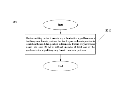
Fig.2 is a schematic flow chart of a synchronous signal transmission method
200
according to the embodiment of this application. As shown in Fig.2, the method
200 may
include the following contents:
S210, the transmitting device transmits a synchronization signal block on a
first
frequency domain position, the first frequency domain position is located on
the candidate
position in frequency domain of synchronous signal, and each 20 MHz subband
includes at
least one of the synchronization signal frequency domain candidate positions.
Optionally, the transmitting device may be a network device, for example, a
network
device as shown in Fig.1
It should be noted that the frequency domain candidate positions of the
synchronization
signals may be the SS raster on the unlicensed frequency bands.
It should be noted that, in the design of the candidate positions in frequency
domain of
synchronous signals, considering that the PDCCH and the synchronous signal
block multiplex
the frequency domain in the unlicensed frequency band, and the frequency
domain granularity
of the basic constituent unit of PDCCH needs six consecutive RBs, when
designing the
synchronous signal block positions within 20M bandwidth, it needs to be
ensured that after
removing the frequency bandwidth occupied by synchronous signal blocks within
20M
bandwidth so that the remaining part shall be continuous 6 RBs or integer
multiples of 6 RBs.
Optionally, in the embodiment of this application, the first frequency domain
position can
satisfy the following three situations:
In case 1, the first frequency domain position is the center frequency point
position of the
synchronization signal block;
In case 2, the first frequency domain position is the position of the resource
element (RE)
with the smallest number in the resource block (RB) with the smallest number
of the
synchronous signal block;
In case 3, the first frequency domain position is the position of the RE with
the largest
number in the RB with the largest number of the synchronous signal block.
Optionally, as an example 1, the first frequency domain position satisfies the
case 1, that
is, the first frequency domain position is the center frequency point position
of the
synchronization signal block.
Optionally, in example 1, the transmitting device determines the frequency
domain
candidate position of the synchronization signal according to formula 2,
fc = fl+(g*20) + f2
Formula 2
8
Date Recue/Date Received 2021-03-04
CA 03111645 2021-03-04
wherein,
fc is the candidate position in frequency domain of synchronous signal,
fl is the center frequency point position of the first 20MHz subband of the
unlicensed
frequency band,
fl + (g*20) is the center frequency point position of the (g+1 )th 20MHz
subband of the
unlicensed frequency band, and G is an integer,
f2 is the offset of the candidate position of the center frequency point of
the synchronous
signal within a 20MHz subband.
Optionally, in example 1, the value of the f2 is at least one of 180hz, -
180kHz; or
the value of the 12 is at least one of 0Hz, 360hz and -360kHz.
Optionally, in example 1, the transmitting device determines that the f2 is at
least one
value satisfying any one of the formulas in formulas 3, 4, 5 and 6.
f2 = (25.5 -(6N + 10)) * 12 * 30kHz
Formula 3
wherein 0 n 5.
12 = (53 -(6N + 10)) * 12 * 15KHz Formula 4
wherein 0 n 14.
12 = (26 -(6N + 10)) * 12 * 30kHz
Formula 5
wherein 0 n 5.
12 = (25 -(6N + 10)) * 12 * 30kHz
Formula 6
wherein 0 n 5.
It should be noted that the Formula 3 is applicable to the scenario that the
20MHz
unlicensed bandwidth includes 51 30kHz RBS, the subcarrier spacing is 30kHz,
and the
center points of 51 30kHz RBs are 25.5 30kHz RBs.
The Formula 4 is applicable to the scenario that 20MHz unlicensed bandwidth
includes
106 15KHz RBs, the subcarrier spacing is 15KHz, and the center points of 106
15kHz RBs
are 53 15kHz RBs.
9
Date Recue/Date Received 2021-03-04
CA 03111645 2021-03-04
The Formula 5 is applicable to the scenario that 20MHz unlicensed bandwidth
includes
51 30kHz RBs, the subcarrier spacing is 30kHz, and the center points of 51
30kHz RBS are
rounded up to 26 30kHz RBs.
The Formula 5 is applicable to the scenario that 20MHz unlicensed bandwidth
includes
51 30kHz RBs, the subcarrier spacing is 30kHz, and the center points of 51
30kHz RBS are
rounded down to 25 30kHz RBs.
Optionally, in example 1, the transmitting device determines that the f2
satisfies at least
one value according to formula 7 or formula 8.
f2 = (Nbw/2 -(6N + Nssb/2)) * Nse* AF kHz
Formula 7
Wherein, Nbw is the number of RBs within the 20MHz bandwidth when the
subcarrier
spacing is AF, Nssbis the number of RbBs occupied by synchronous signal block
in frequency
domain, Nse is the number of subcarriers in one RB, and N is an integer.
f2 = ((Nbw 1)/2 -(6N + Nssb/2)) * Nse* Af kHz
Formula 8
Wherein, Nbw is the number of RBs within 20MHz bandwidth when the subcarrier
spacing is AF, Nssb is the number of RBs occupied by synchronous signal block
in frequency
domain, Nse is the number of subcarriers in one RB, and N is an integer.
Optionally, in example 1, the value of the f2 is at least one of 5580kHz,
3420kHz,
1260kHz, -900kHz, -3060kHz and -5220kHz; or the value of the f2 is at least
one of 5220kHz,
3060kHz, 900kHz, -1260kHz, -3420kHz and -5580kHz; or the value of the f2 is at
least one
of 5760kHz, 3600kHz, 1440kHz, -720kHz, -2880kHz and -5040kHz; or the value of
the f2 is
at least one of 5040kHz, 2880kHz, 720kHz, -1440kHz, -3600kHz and -5760kHz; or
the value
of THE F2 is at least one of 5400kHz, 3240kHz, 1080kHz, -1080kHz, -3240kHz and
-5400kHz.
Optionally, as example 2, the first frequency domain position satisfies the
case 2. That is,
the first frequency domain position is the position of the RE with the
smallest number in the
RB with the smallest number of the synchronous signal block.
Optionally, in example 2, the transmitting device determines the frequency
domain
candidate position of the synchronization signal according to formula 9,
fc= fl+(g*20) + f2 + 3
Formula 9
Wherein,
fc is the candidate position in frequency domain of synchronous signal,
Date Recue/Date Received 2021-03-04
CA 03111645 2021-03-04
fl is the center frequency point position of the first 20MHz subband of the
unlicensed
frequency band,
fl + (g*20) is the center frequency point position of the (g+l)th 20MHz
subband of the
unlicensed frequency band, and g is an integer,
f2 is the offset of the candidate position of the center frequency point of
the synchronous
signal within a 20MHz subband,
3 is the offset of the position of the RE with the smallest number in the RB
with the
smallest number of the synchronous signal block from the position of the
center frequency
point of the synchronous signal block.
Optionally, in example 2,
the value of the f2 is at least one of 180hz, -180kHz; or
the value of the f2 is at least one of 0Hz, 360hz and -360kHz.
Optionally, in example 2, the transmitting device determines that the f2 is at
least one
value satisfying any one of the formulas 3, 4, 5 and 6.
Optionally, in example 2, the transmitting device determines that the f2
satisfies at least
one value according to the formula 7 or formula 8.
Optionally, in example 2, the value of the f2 is at least one of 5580kHz,
3420kHz,
1260kHz, -900kHz, -3060kHz and -5220kHz; or the value of the f2 is at least
one of 5220kHz,
3060kHz, 900kHz, -1260kHz, -3420kHz and -5580kHz; or the value of the f2 is at
least one
of 5760kHz, 3600kHz, 1440kHz, -720kHz, -2880kHz and -5040kHz; or the value of
the f2 is
at least one of 5040kHz, 2880kHz, 720kHz, -1440kHz, -3600kHz and -5760kHz; or
the value
of the f2 is at least one of 5400kHz, 3240kHz, 1080kHz, -1080kHz, -3240kHz and
-5400kHz.
Optionally, in example 2,
If the synchronous signal block occupies 20 RBs in the frequency domain, and
the
subcarrier spacing of the synchronous signal blocks is 30kHz, the transmitting
device
determines that the 3 = -3600kHz; or
If the synchronous signal block occupies 20 RBs in the frequency domain, and
the
subcarrier spacing of the synchronous signal blocks is 15 kHz, the transmitter
determines that
the 3 = -1800kHz.
Optionally, as example 3, the first frequency domain position satisfies case
3. That is, the
first frequency domain position is the position of the RE with the largest
number in the RB
with the largest number of the synchronous signal block.
11
Date Recue/Date Received 2021-03-04
CA 03111645 2021-03-04
Optionally, in example 3, the transmitting device determines the frequency
domain
candidate position of the synchronization signal according to formula 10,
fc= fl + (g*20) + f2 + f4
Formula 10
Wherein,
fc is the candidate position in frequency domain of synchronous signal,
fl is the center frequency point position of the first 20MHz subband of the
unlicensed
frequency band,
fl + (g*20) is the center frequency point position of the (g+1 )th 20MHz
subband of the
unlicensed frequency band, and g is an integer,
f2 is the offset of the candidate position of the center frequency point of
the synchronous
signal within a 20MHz subband,
f4 is the offset of the position of the RE with the largest number in the RB
with the largest
number of the synchronous signal block from the center frequency point of the
synchronous
signal block.
Optionally, in example 3,
the value of the f2 is at least one of 180hz, -180kHz; or
the value of the f2 is at least one of 0Hz, 360hz and -360kHz.
Optionally, in example 3, the transmitting device determines that the f2 is at
least one
value satisfying any one of the formulas 3, 4, 5 and 6.
Optionally, in example 3, the transmitting device determines that the f2
satisfies at least
one value according to the formula 7 or formula 8.
Optionally, in example 3, the value of the f2 is at least one of 5580kHz,
3420kHz,
1260kHz, -900kHz, -3060kHz and -5220kHz; or the value of the f2 is at least
one of 5220kHz,
3060kHz, 900kHz, -1260kHz, -3420kHz and -5580kHz; or the value of the f2 is at
least one
of 5760kHz, 3600kHz, 1440kHz, -720kHz, --2880kHz and -5040kHz; or the value of
the f2 is
at least one of 5040kHz, 2880kHz, 720kHz, -1440kHz, -3600kHz and -5760kHz; or
the value
of the f2 is at least one of 5400kHz, 3240kHz, 1080kHz, -1080kHz, -3240kHz and
-5400kHz.
Optionally, in example 3,
If the synchronous signal block occupies 20 RBs in the frequency domain, and
the
subcarrier spacing of the synchronous signal block is 30 kHz, the transmitting
device
determines that the f4 = 3600kHz; or
12
Date Recue/Date Received 2021-03-04
CA 03111645 2021-03-04
If the synchronous signal block occupies 20 RBs in the frequency domain, and
the
subcarrier spacing of the synchronous signal block is 15 kHz, the transmitting
device
determines that the f4 = 1800 kHz.
Optionally, as an embodiment 1, the first frequency domain position is the
center
frequency point position of the synchronization signal block. That is, the
transmitting device
determines the frequency domain candidate position of the synchronization
signal according
to the Formula 2.
Specifically, as shown in Fig.3, in the embodiment 1, the values of parameters
in Formula
2 are as follows:
fl = 5160mhz, which is the center frequency point of the first 20MHz subband
of the
unlicensed frequency band;
fl+(g*20) is the center frequency position of the (g+l)th 20MHz subband of the
unlicensed frequency band, and g is an integer;
f2= -(25.5-(6*3+10))*12*30kHz=900kHz.
To sum up, it is concluded that the frequency domain candidate positions of
the
synchronous signal are: fc = 5160.9 + (g * 20) MHz, and g is an integer.
It should be noted that, as shown in Fig.3, in additional to the 20 30kHz RBs
occupied by
the synchronous signal block, there are 18 30kHz continuous RBs. The 18 30kHz
RBs can
ensure the PDCCH transmission. That is, the multiplexing in frequency domain
of PDCCH
and synchronous signal block is realized.
Specifically, in the embodiment 1, when the network device transmits the
synchronization
signal on the unlicensed frequency band, the synchronization signal block
occupies 20 30kHz
RB in the frequency domain (referring to the area represented by the shaded
part in Fig.3),
and the network device selects one or more frequency points from the frequency
points
corresponding to fc to send the synchronous signal block. The central
frequency point of the
synchronization signal block is located in the frequency point selected by the
network device.
When the terminal device conducts cell search on the unlicensed frequency
band, it tries to
search the synchronization signal on the frequency points corresponding to fc.
Optionally, as an embodiment 2, the first frequency domain position is the
center
frequency point position of the synchronization signal block. That is, the
transmitting device
determines the frequency domain candidate position of the synchronization
signal according
to the Formula 2.
13
Date Recue/Date Received 2021-03-04
CA 03111645 2021-03-04
Specifically, as shown in Fig.4, in the embodiment 2, the values of parameters
in Formula
2 are as follows:
fl = 5160 MHz, which is the center frequency point of the first 20MHz subband
of the
unlicensed frequency band;
fl + (g*20) is the center frequency position of the (g+l)th 20MHz subband of
the
unlicensed frequency band, and g is an integer;
f2=(25.5-(6*2+10))*12*30 kHz=1260kHz.
To sum up, it is concluded that the frequency domain candidate positions of
the
synchronous signal are: fc=5161.26+(g*20) MHz, g is an integer.
It should be noted that, as shown in Fig.4, in additional to the 20 30kHz RBs
occupied by
the synchronous signal block, there are 12 30kHz continuous RBs. The 12 30kHz
RBs can
ensure the PDCCH transmission. That is, the multiplexing in frequency domain
of PDCCH
and synchronous signal block is realized.
Specifically, in embodiment 2, when the network device transmits the
synchronization
signal on the unlicensed frequency band, the synchronization signal block
occupies 20 30 kHz
RBs in the frequency domain (referring to the area represented by the shaded
part in Fig.4),
and the network device selects one or more frequency points from the frequency
points
corresponding to fc to send the synchronous signal block. The central
frequency point of the
synchronization signal block is located on the frequency point selected by the
network device.
When the terminal device conducts cell search on the unlicensed frequency
band, it tries to
search the synchronization signal on the corresponding frequency points
corresponding to fc.
Optionally, as an embodiment 3, the first frequency domain position is the
center
frequency point position of the synchronization signal block. That is, the
transmitting device
determines the frequency domain candidate position of the synchronization
signal according
to the Formula 2.
Specifically, as shown in Fig.5, in the third embodiment, the values of
parameters in
Formula 2 are as follows:
fl = 5160 MHz, which is the center frequency point of the first 20MHz subband
of the
unlicensed frequency band;
fl+(g*20) is the center frequency position of the (g+l)th 20MHz subband of the
unlicensed frequency band, and g is an integer;
f2=-180kHz.
14
Date Recue/Date Received 2021-03-04
CA 03111645 2021-03-04
To sum up, it is concluded that the frequency domain candidate positions of
the
synchronous signal are: fc = 5159.82 + (g * 20) MHz, and g is an integer.
Specifically, in the embodiment 3, when the network device transmits the
synchronization
signal on the unlicensed frequency band, the synchronization signal block
occupies 20 30 kHz
RBs in the frequency domain (referring to the area represented by the shaded
part in Fig.5),
and the network device selects one or more frequency points from the frequency
points
corresponding to fc to send the synchronous signal block. The central
frequency point of the
synchronization signal block is located on the frequency point selected by the
network device.
When the terminal device conducts cell search on the unlicensed frequency
band, it tries to
search the synchronization signal on the corresponding frequency points
corresponding to fc.
Optionally, as an embodiment 4, the first frequency domain position is the
center
frequency point position of the synchronization signal block. That is, the
transmitting device
determines the frequency domain candidate positions of the synchronization
signal according
to the Formula 2.
Specifically, as shown in Fig.6, in the embodiment 4, the values of parameters
in Formula
2 are as follows:
fl = 5160mhz, which is the center frequency point of the first 20MHz subband
of the
unlicensed frequency band;
fl + (g*20) is the center frequency position of the (g+l)th 20MHz subband of
the
unlicensed frequency band, and g is an integer;
f2=(26-(6*2+10))*12*30 kHz=1440kHz.
To sum up, it is concluded that the frequency domain candidate positions of
the
synchronous signal are fc = 5161.44 + (g * 20) MHz, and g is an integer.
It should be noted that, as shown in Fig.6, there are 12 30kHz continuous RBS
outside the
20 30kHz RBS occupied by the synchronous signal block. These 12 30kHz RBS can
ensure
the transmission of PDCCH, that is, the multiplexing in frequency domain of
PDCCH and
synchronous signal block is realized.
Specifically, in the embodiment 4, when the network device transmits the
synchronization
signal on the unlicensed frequency band, the synchronization signal block
occupies 20 30 kHz
RBs in the frequency domain (referring to the area represented by the shaded
part in Fig.6),
and the network device selects one or more frequency points from the frequency
points
corresponding to fc to send the synchronous signal block. The central
frequency point of the
synchronization signal block is located on the frequency point selected by the
network device.
Date Recue/Date Received 2021-03-04
CA 03111645 2021-03-04
When the terminal device conducts cell search on the unlicensed frequency
band, it tries to
search the synchronization signal on the corresponding frequency points
corresponding to fc.
Optionally, as an embodiment 5, the first frequency domain position is the
center
frequency point position of the synchronization signal block. That is, the
transmitting device
determines the frequency domain candidate positions of the synchronization
signal according
to the Formula 2.
Specifically, as shown in Fig.7, in the embodiment 5, the values of parameters
in formula
2 are as follows:
fl = 5160mhz, which is the center frequency point of the first 20MHz subband
of the
unlicensed frequency band;
fl+(g*20) is the center frequency position of the (g+l)th 20MHz subband of the
unlicensed frequency band, and G is an integer;
f2=-(26-(6*3+10))*12*30 kHz=720kHz.
To sum up, it is concluded that the frequency domain candidate positions of
the
synchronous signal are: fc = 5160.72 + (g * 20) MHz, and G is an integer.
It should be noted that, as shown in Fig.7, in additional to the 20 30kHz RBs
occupied by
the synchronous signal block, there are 18 30kHz continuous RBs. The 18 30kHz
RBS can
ensure the PDCCH transmission. That is, the multiplexing in frequency domain
of PDCCH
and synchronous signal block is realized.
Specifically, in the embodiment 5, when the network device transmits the
synchronization
signal on the unlicensed frequency band, the synchronization signal block
occupies 20 30 kHz
RBs in the frequency domain (referring to the area represented by the shaded
part in Fig.7),
and the network device selects one or more frequency points from the frequency
points
corresponding to fc to send the synchronous signal block. The central
frequency point of the
synchronization signal block is located on the frequency point selected by the
network device.
When the terminal device conducts cell search on the unlicensed frequency
band, it tries to
search the synchronization signal on the corresponding frequency points
corresponding to fc.
Optionally, as an embodiment 6, the first frequency domain position is the
center
frequency point position of the synchronization signal block. That is, the
transmitting device
determines the frequency domain candidate position of the synchronization
signal according
to the Formula 2.
Specifically, as shown in Fig.8, in the embodiment 6, the values of parameters
in Formula
2 are as follows:
16
Date Recue/Date Received 2021-03-04
CA 03111645 2021-03-04
fl = 5160mhz, which is the center frequency point of the first 20MHz subband
of the
unlicensed frequency band;
fl+(g*20) is the center frequency position of the (g+l)th 20MHz subband of the
unlicensed frequency band, and G is an integer;
f2=(25-(6*2+10))*12*30 kHz=1080kHz.
To sum up, it is concluded that the frequency domain candidate positions of
the
synchronous signal are: fc = 5161.08 + (g * 20) MHz, and g is an integer.
It should be noted that, as shown in Fig.8, in additional to the 20 30kHz RBS
occupied by
the synchronous signal block, there are 12 30kHz continuous RBS. The 12 30kHz
RBS can
ensure the PDCCH transmission. That is, the multiplexing in frequency domain
of PDCCH
and synchronous signal block is realized.
Specifically, in the embodiment 6, when the network device transmits the
synchronization
signal on the unlicensed frequency band, the synchronization signal block
occupies 20 30 kHz
RBs in the frequency domain (referring to the area represented by the shaded
part in Fig.8),
and the network device selects one or more frequency points from the frequency
points
corresponding to fc to send the synchronous signal block. The central
frequency point of the
synchronization signal block is located on the frequency point selected by the
network device.
When the terminal device conducts cell search on the unlicensed frequency
band, it tries to
search the synchronization signal on the corresponding frequency points
corresponding to fc.
Optionally, as tan embodiment 7, the first frequency domain position is the
center
frequency point position of the synchronization signal block, that is, the
transmitting device
determines the frequency domain candidate position of the synchronization
signal according
to the Formula 2.
Specifically, as shown in Fig.9, in the embodiment 7, the values of parameters
in formula
2 are as follows:
fl = 5160mhz, which is the center frequency point of the first 20MHz subband
of the
unlicensed frequency band;
fl+(g*20) is the center frequency position of the (g+l)th 20MHz subband of the
unlicensed frequency band, and g is an integer;
f2=0kHz.
To sum up, it is concluded that the frequency domain candidate positions of
the
synchronous signal are: fc = 5160 + (g * 20) MHz, and g is an integer.
17
Date Recue/Date Received 2021-03-04
CA 03111645 2021-03-04
Specifically, in the embodiment 7, when the network device transmits the
synchronization
signal on the unlicensed frequency band, the synchronization signal block
occupies 20 30kHz
RBs in the frequency domain (referring to the area represented by the shaded
part in Fig.9),
and the network device selects one or more frequency points from the frequency
points
corresponding to fc to send the synchronous signal block. The central
frequency point of the
synchronization signal block is located on the frequency point selected by the
network device.
When the terminal device conducts cell search on the unlicensed frequency
band, it tries to
search the synchronization signal on the corresponding frequency points
corresponding to fc.
It should be understood that, in the embodiments 1 to 7 stated above, it is an
example that
the first frequency domain position is the center frequency point position of
the
synchronization signal block. The first frequency domain position is the
position of the RE
with the smallest number in the R) with the smallest number of the synchronous
signal block
(corresponding to Formula 9). And t the first frequency domain position is the
position of the
RE with the largest number in the RB with the largest number of the
synchronous signal block
(corresponding to formula 10). For brevity, details are not described herein
again.
It should also be understood that, in the embodiments 1 to 7 stated above, it
is an example
for illustration that a 20MHz unlicensed bandwidth includes 51 30kHz RBs, and
the
subcarrier spacing is 30kHz. The scenario of a 20MHz unlicensed bandwidth
including 106
15kHz RBs and the subcarrier spacing being 15kHz is also applicable. For
brevity, details are
not described herein again.
Therefore, in the embodiments of this application, the frequency domain
candidate
position of the synchronization signal on the unlicensed frequency band (also
called SS raster)
is designed, which can reduce the complexity of the cell initially searching
and reduce the
influence of the position, where a cell in the unlicensed frequency band
initially access the
synchronization signal block in the subband, on the other channels in the
subband.
Fig.10 is a schematic flow chart of a synchronous signal transmission method
300
according to an embodiment of this application. As shown in FIG.10, the method
300 may
include the following contents:
S310, the receiving device monitors a synchronization signal block on a first
frequency
domain position, the first frequency domain position is located on the
candidate positions in
frequency domain of the synchronous signals, and each 20 MHz subband includes
at least one
of the synchronization signal frequency domain candidate positions.
Optionally, the receiving device is a terminal device, for example, the
erminal device
shown in Fig.1.
18
Date Recue/Date Received 2021-03-04
CA 03111645 2021-03-04
Optionally, in the embodiment of this application, the first frequency domain
position can
satisfy the following three situations:
In case 1, the first frequency domain position is the center frequency point
position of the
synchronization signal block;
In case 2, the first frequency domain position is the position of the RE with
the smallest
number in the RB with the smallest number of the synchronous signal block;
In case 3, the first frequency domain position is the position of the RE with
the largest
number in the RB with the largest number of the synchronous signal block.
Optionally, the first frequency domain position is the center frequency point
position of
the synchronization signal block.
Optionally, as an example 1, the first frequency domain position satisfies
case 1, that is,
the first frequency domain position is the center frequency point position of
the
synchronization signal block.
Optionally, in example 1, the receiving device determines the frequency domain
candidate position of the synchronization signal according to the formula fc =
fl+(g*20) + f2,
wherein,
fc is the candidate position in frequency domain of synchronous signal,
fl is the center frequency point position of the first 20MHz subband of the
unlicensed
frequency band,
fl+(g*20) is the center frequency point position of the (g+l)th 20MHz subband
of the
unlicensed frequency band, and g is an integer,
f2 is the offset of the candidate position of the center frequency point of
the synchronous
signal within a 20MHz subband.
Optionally, in example 1, the value of f2 is at least one of 180hz, -180kHz;
or
the value of the f2 is at least one of 0Hz, 360Hz and -360kHz.
Optionally, in example 1,
the receiving device determines that the f2 is at least one of the values
satisfying the
formula f2= (Nbw/2-(6n+Nssb/2))*Nse*AF kHz,
wherein, Nbw is the RB number in 20MHz bandwidth when the subcarrier spacing
is AF,
Nssb is the RB number occupied by the synchronous signal block in frequency
domain, Nse is
the subcarrier number in one RB, and N is an integer.
19
Date Recue/Date Received 2021-03-04
CA 03111645 2021-03-04
Optionally, in example 1,
the receiving device determines that the f2 is at least one of the values
satisfying the
formula f2= ((Nbw 1)/2-(6n+Nssb/2))*Nse*AF kHz,
wherein, Nbw is the RB number in 20MHz bandwidth when the subcarrier spacing
is AF,
Nssb is the RB number occupied by the synchronous signal block in frequency
domain, Nse is
the subcarrier number in one RB, and N is an integer.
Optionally, in example 1,
the receiving device determines that the f2 is at least one of the values
satisfying the
formula f2= (25.5-(6n+10))*12*30kHz, 0<n<5; or
the receiving device determines that the f2 is at least one of the values
satisfying the
formula f2= (53-(6n+10))*12*15KHz, On 14; or
the receiving device determines that the f2 is at least one of the values
satisfying the
formula f2= (26-(6n+10))*12*30kHz, On 5; or
the receiving device determines that the f2 is at least one of the values
satisfying the
formula f2= (25-(6n+10))*12*30kHz, On 5.
Optionally, in example 1, the value of the f2 is at least one of 5580kHz,
3420kHz,
1260kHz, -900kHz, -3060kHz and -5220kHz; or the value of the f2 is at least
one of 5220kHz,
3060kHz, 900kHz, -1260kHz, -3420kHz and -5580kHz; or the value of the f2 is at
least one
of 5760kHz, 3600kHz, 1440kHz, -720kHz, -2880kHz and -5040kHz; or the value of
the f2 is
at least one of 5040kHz, 2880kHz, 720kHz, -1440kHz, -3600kHz and -5760kHz; or
the value
of the f2 is at least one of 5400kHz, 3240kHz, 1080kHz, -1080kHz, -3240kHz and
-5400kHz.
Optionally, as example 2, the first frequency domain position satisfies the
case 2. That is,
the first frequency domain position is the position of the RE with the
smallest number in the
RB with the smallest number of the synchronous signal block.
Optionally, in example 2, the receiving device determines the frequency domain
candidate position of the synchronization signal according to the formula fc =
fl+(g*20) + f2
+ f3,
Wherein,
fc is the candidate position in frequency domain of synchronous signal,
fl is the center frequency point position of the first 20MHz subband of the
unlicensed
frequency band,
Date Recue/Date Received 2021-03-04
CA 03111645 2021-03-04
fl+(g*20) is the center frequency point position of the (g+l)th 20MHz subband
of the
unlicensed frequency band, and g is an integer,
f2 is the offset position of the candidate position of the center frequency
point of the
synchronous signal in a 20MHz subband,
3 is the offset of the position of the RE with the smallest number in the RB
with the
smallest number of the synchronous signal block from the position of the
center frequency
point of the synchronous signal block.
Optionally, in example 2, the value of the f2 is at least one of 180hz, -
180kHz; or
the value of the f2 is at least one of 0Hz, 360Hz and -360kHz.
Optionally, in example 2,
the receiving device determines that the f2 is at least one of the values
satisfying the
formula f2= (Nbw/2-(6n+Nssb/2))*Nse*AF kHz,
wherein, Nbw is the RB number in 20MHz bandwidth when the subcarrier spacing
is AF,
Nssb is the RB number occupied by the synchronous signal block in frequency
domain, Nse is
the subcarrier number in one RB, and N is an integer.
Optionally, in example 2,
the receiving device determines that the f2 is at least one of the values
satisfying the
formula f2= ((Nbw 1)/2-(6n+Nssb/2))*Nse*AF kHz,
wherein, Nbw is the RB number in 20MHz bandwidth when the subcarrier spacing
is AF,
Nssb is the RB number occupied by the synchronous signal block in frequency
domain, Nse is
the subcarrier number in one RB, and N is an integer.
Optionally, in example 2,
the receiving device determines that the f2 is at least one of the values
satisfying the
formula f2= (25.5-(6n+10))*12*30kHz, 0<n<5; or
the receiving device determines that the f2 is at least one of the values
satisfying the
formula f2= (53-(6n+10))*12*15KHz, On 14; or
the receiving device determines that the f2 is at least one of the values
satisfying the
formula f2= (26-(6n+10))*12*30kHz, On 5; or
the receiving device determines that the f2 is at least one of the values
satisfying the
formula f2= (25-(6n+10))*12*30kHz, On 5.
21
Date Recue/Date Received 2021-03-04
CA 03111645 2021-03-04
Optionally, in example 2, the value of the f2 is at least one of 5580kHz,
3420kHz,
1260kHz, -900kHz, -3060kHz and -5220kHz; or the value of the f2 is at least
one of 5220kHz,
3060kHz, 900kHz, -1260kHz, -3420kHz and -5580kHz; or the value of the f2 is at
least one
of 5760kHz, 3600kHz, 1440kHz, -720kHz, -2880kHz and -5040kHz; or the value of
the f2 is
at least one of 5040kHz, 2880kHz, 720kHz, -1440kHz, -3600kHz and -5760kHz; or
the value
of the f2 is at least one of 5400kHz, 3240kHz, 1080kHz, -1080kHz, -3240kHz and
-5400kHz.
Optionally, in example 2,
if the synchronous signal block occupies 20 RBs in the frequency domain, and
the
subcarrier spacing of the synchronous signal blocks is 30kHz, the transmitting
device
determines that the 3 = -3600kHz; or
if the synchronous signal block occupies 20 RBs in the frequency domain, and
the
subcarrier spacing of the synchronous signal blocks is 15 kHz, the transmitter
determines that
the 3 = -1800kHz.
Optionally, as example 3, the first frequency domain position satisfies the
case 3. That is,
the first frequency domain position is the position of the RE with the largest
number in the RB
with the largest number of the synchronous signal block.
Optionally, in example 3, the receiving device determines the frequency domain
candidate position of the synchronization signal according to the formula fc =
fl+(g*20) + f2
+ f4,
Wherein,
fc is the candidate position in frequency domain of synchronous signal,
fl is the center frequency point position of the first 20MHz subband of the
unlicensed
frequency band,
fl+(g*20) is the center frequency point position of the (g+l)th 20MHz subband
of the
unlicensed frequency band, and G is an integer,
f2 is the offset of the candidate position of the center frequency point of
the synchronous
signal in a 20MHz subband,
f4 is the offset of the position of the RE with the largest number in the RB
with the largest
number of the synchronous signal block from the center frequency point of the
synchronous
signal block.
Optionally, in example 3,
the value of the f2 is at least one of 180hz, -180kHz; or
22
Date Recue/Date Received 2021-03-04
CA 03111645 2021-03-04
the value of the f2 is at least one of 0Hz, 360hz and -360kHz.
Optionally, in example 3,
the receiving device determines that the f2 is at least one of the values
satisfying the
formula f2 = (Nbw/2 -(6n + Nssb/2)) * Nse* Af kHz,
wherein, Nbw is the RB number in 20MHz bandwidth when the subcarrier spacing
is AF,
Nssb is the RB number occupied by synchronous signal block in frequency
domain, NseNis the
number of subcarriers in one RB, and N is an integer.
Optionally, in example 3,
the receiving device determines that the f2 is at least one of the values
satisfying the
formula f2 = ((Nbw 1)/2 -(6n +Nssb/2)) * Nse* Af kHz,
wherein Nbw is the RB number in 20MHz bandwidth when the subcarrier spacing is
AF,
Nssb is the RB number occupied by synchronous signal block in frequency
domain, Nse is the
number of subcarriers in one RbB, and N is an integer.
Optionally, in example 3,
the receiving device determines that the f2 is at least one of the values
satisfying the
formula f2= (25.5-(6n+10))*12*30kHz, 0<n<5; or
the receiving device determines that the f2 is at least one of the values
satisfying the
formula f2= (53-(6n+10))*12*15KHz, On 14; or
the receiving device determines that the f2 is at least one of the values
satisfying the
formula f2= (26-(6n+10))*12*30kHz, On 5; or
the receiving device determines that the f2 is at least one of the values
satisfying the
formula f2= (25-(6n+10))*12*30kHz, On 5.
Optionally, in example 3, the value of the f2 is at least one of 5580kHz,
3420kHz,
1260kHz, -900kHz, -3060kHz and -5220kHz; or the value of f2 is at least one of
5220kHz,
3060kHz, 900kHz, -1260kHz, -3420kHz and -5580kHz; or the value of the f2 is at
least one
of 5760kHz, 3600kHz, 1440kHz, -720kHz, -2880kHz and -5040kHz; or the value of
the f2 is
at least one of 5040kHz, 2880kHz, 720kHz, -1440kHz, -3600kHz and -5760kHz; or
the value
of the f2 is at least one of 5400kHz, 3240kHz, 1080kHz, -1080kHz, -3240kHz and
-5400kHz.
23
Date Recue/Date Received 2021-03-04
CA 03111645 2021-03-04
Optionally, in example 3,
if the synchronous signal block occupies 20 RBs in the frequency domain, and
the
subcarrier spacing of the synchronous signal blocks is 30kHz, the transmitting
device
determines that the f4 = 3600kHz; or
if the synchronous signal block occupies 20 RBs in the frequency domain, and
the
subcarrier spacing of the synchronous signal blocks is 15 kHz, the transmitter
determines that
the f4 = 1800 kHz.
It should be understood that the steps in the method 300 of synchronous signal
transmission can refer to the corresponding steps in the method 200 of
synchronous signal
transmission. For brevity, details are not described herein again.
Therefore, in the embodiments of this application, the frequency domain
candidate
position of the synchronization signal on the unlicensed frequency band (also
called SS raster)
is designed, which can reduce the complexity of the cell initially searching
and reduce the
influence of the position, where a cell in the unlicensed frequency band
initially access the
synchronization signal block in the subband, on the other channels in the
subband.
Fig.11 shows a schematic block diagram of a transmitting device 400 according
to an
embodiment of this application. As shown in FIG.11, the transmitting device
400 includes:
a communication unit 410, configured to transmit a synchronization signal
block at a first
frequency domain position located on a frequency domain candidate position of
a
synchronous signal, and each 20 MHz subband includes at least one frequency
domain
candidate position of the synchronization signal.
Optionally, the first frequency domain position is the center frequency point
position of
the synchronization signal block.
Optionally, the transmitting device 400 further includes:
a processing unit 420, configured to determine the frequency domain candidate
position
of the synchronization signal according to the formula fc = fl+(g*20) + f2,
wherein,
fc is the candidate position in frequency domain of synchronous signal,
fl is the center frequency point position of the first 20MHz subband of the
unlicensed
frequency band,
fl+(g*20) is the center frequency point position of the (g+l)th 20MHz subband
of the
unlicensed frequency band, and g is an integer,
24
Date Recue/Date Received 2021-03-04
CA 03111645 2021-03-04
f2 is the offset of the candidate position of the center frequency point of
the synchronous
signal within a 20MHz subband.
Optionally, the transmitting device 400 further includes:
a processing unit 420, configured to determine the frequency domain candidate
position
of the synchronous signal according to the formula fc = fl+(g*20) + f2 + 3,
wherein,
fc is the candidate position in frequency domain of synchronous signal,
fl is the center frequency point position of the first 20MHz subband of the
unlicensed
frequency band,
fl+(g*20) is the center frequency point position of the (g+l)th 20MHz subband
of the
unlicensed frequency band, and g is an integer,
f2 is the offset of the candidate position of the center frequency point of
the synchronous
signal in a 20MHz subband,
3 is the offset of the position of the RE with the smallest number in the RB
with the
smallest number of the synchronous signal block from the position of the
center frequency
point of the synchronous signal block.
Optionally, the processing unit 420 is further configured to:
determine the 13= -3600kHz if the synchronous signal block occupies 20 RBs in
the
frequency domain, and the subcarrier spacing of the synchronous signal blocks
is 30kHz; or
determine the 3 = -1800kHz if the synchronous signal block occupies 20 RBs in
the
frequency domain, and the subcarrier spacing of the synchronous signal blocks
is 15 kHz.
Optionally, the first frequency domain position is the position of the RE with
the largest
number in the RB with the largest number of the synchronous signal block.
Optionally, the transmitting device 400 further includes:
a processing unit 420 is used to determine the frequency domain candidate
position of the
synchronous signal according to the formula fc = fl+(g*20) + f2 + f4,
wherein,
fc is the candidate position in frequency domain of synchronous signal,
fl is the center frequency point position of the first 20MHz subband of the
unlicensed
frequency band,
Date Recue/Date Received 2021-03-04
CA 03111645 2021-03-04
fl+(g*20) is the center frequency point position of the (g+l)th 20MHz subband
of the
unlicensed frequency band, and g is an integer,
f2 is the offset position of the candidate position of the center frequency
point of the
synchronous signal in a 20MHz subband,
f4 is the offset of the position of the RE with the largest number in the RB
with the largest
number of the synchronous signal block from the center frequency point of the
synchronous
signal block.
Optionally, the processing unit 420 is futher configured to:
determine the f4=3600 kHz if the synchronous signal block occupies 20 RBs in
the
frequency domain, and the subcarrier spacing of the synchronous signal blocks
is 30kHz; or
determine the f4=1800 kHz if the synchronous signal block occupies 20 RBs in
the
frequency domain, and the subcarrier spacing of the synchronous signal blocks
is 15 kHz.
Optionally, the value of f2 is at least one of 180hz, -180kHz; or
the value of the f2 is at least one of 0Hz, 360hz and -360kHz.
Optionally, the processing unit 420 is further configured to:
determine that the f2 is at least one of the values satisfying the formula f2
= (Nbw/2 -(6n
+ Nssb/2)) * Nse* Af kHz,
wherein, Nbw is the RB number in 20MHz bandwidth when the subcarrier spacing
is AF,
Nssb is the number of Rb occupied by synchronous signal block in frequency
domain, nseis the
number of subcarriers in one Rb, and N is an integer.
Optionally, the processing unit 420 is further configured to:
determine that the f2 is at least one of the values satisfying the formula f2
= ((Nbw 1)/
2 -(6n + Nssb/2)) * Nse* Af kHz,
wherein, Nbw is the RB number in 20MHz bandwidth when the subcarrier spacing
is AF,
Nssb is the RB number occupied by synchronous signal block in frequency
domain, Nse is the
number of subcarriers in one RB, and N is an integer.
Optionally, the processing unit 420 is further configured to:
determine that the f2 is at least one of the value satisfying the formula f2=
(25.5-(6N+10))*12*30kHz, 0 1.1 5; or
26
Date Recue/Date Received 2021-03-04
CA 03111645 2021-03-04
determine that the f2 is at least one of the values satisfying the formula f2=
(53-(6N+10))*12*15KHz,0 1.1 14; or
determine that the f2 is at least one of the values satisfying the formula f2=
(26-(6N+10))*12*30kHz,0 1.1 5; or
determine that the f2 is at least one of the values satisfying the formula f2=
(25-(6N+10))*12*30kHz,0 1.1 5.
Optionally, the value of the f2 is at least one of 5580kHz, 3420kHz, 1260kHz, -
900kHz,
-3060kHz and -5220kHz; or
The value of the 12 is at least one of 5220kHz, 3060kHz, 900kHz, -1260kHz, -
3420kHz
and -5580kHz; or
The value of the 12 is at least one of 5760kHz, 3600kHz, 1440kHz, -720kHz, -
2880kHz
and -5040kHz; or
The value of the 12 is at least one of 5040kHz, 2880kHz, 720kHz, -1440kHz, -
3600kHz
and -5760kHz; or
The value of the f2 is at least one of 5400kHz, 3240kHz, 1080kHz, -1080kHz, -
3240kHz
and -5400kHz.
Optionally, the transmitting device 400 is a network device.
It should be understood that the transmitting device 400 according to the
embodiment of
this application can correspond to the transmitting device in the embodiments
of the method
of this application, and the above and other operations and/or functions of
each unit in the
transmitting device 400 respectively realize the corresponding processes of
the transmitting
device in the method 200 shown in Fig.2, and will not be described here for
brevity.
Fig.12 shows a schematic block diagram of a receiving device 500 according to
an
embodiment of this application. As shown in FIG.12, the receiving device 500
includes:
a communication unit 510, configured to monitor for a synchronization signal
block at a
first frequency domain position, which is located on the frequency domain
candidate position
of the synchronization signal, wherein each 20 MHz subband includes at least
one frequency
domain candidate position of the synchronization signal.
27
Date Recue/Date Received 2021-03-04
CA 03111645 2021-03-04
Optionally, the first frequency domain position is the center frequency point
position of
the synchronization signal block.
The receiving device 500 further includes:
a processing unit 520, configured to determine the frequency domain candidate
position
of the synchronous signal according to the formula fc = fl+(g*20) + 12,
wherein,
fc is the candidate position in frequency domain of synchronous signal,
fl is the center frequency point position of the first 20MHz subband of the
unlicensed
frequency band,
fl+(g*20) is the center frequency point position of the (g+l)th 20MHz subband
of the
unlicensed frequency band, and g is an integer,
f2 is the offset position of the candidate position of the center frequency
point of the
synchronous signal in a 20MHz subband.
Optionally, the first frequency domain position is the position of the RE with
the smallest
number of the RB with the smallest number in the synchronization signal block.
The receiving device 500 further includes:
a processing unit 520, configured to determine the frequency domain candidate
position
of the synchronous signal according to the formula fc = fl+(g*20) + f2 + 3,
wherein,
fc is the candidate position in frequency domain of synchronous signal,
fl is the center frequency point position of the first 20MHz subband of the
unlicensed
frequency band,
fl+(g*20) is the center frequency point position of the (g+l)th 20MHz subband
of the
unlicensed frequency band, and g is an integer,
f2 is the offset position of the candidate position of the center frequency
point of the
synchronous signal in a 20MHz subband,
3 is the offset of the position of the RE with the smallest number in the RB
with the
smallest number in the synchronous signal block from the position of the
center frequency
point of the synchronous signal block.
28
Date Recue/Date Received 2021-03-04
CA 03111645 2021-03-04
Optionally, the processing unit 520 is further configured to:
determine the f3=-3600 kHz if the synchronous signal block occupies 20 RBs in
the
frequency domain, and the subcarrier spacing of the synchronous signal blocks
is 30kHz; or
determine the f3=-1800 kHz if the synchronous signal block occupies 20 RBs in
the
frequency domain, and the subcarrier spacing of the synchronous signal blocks
is 15 kHz.
Optionally, the first frequency domain position is the position of the RE with
the largest
number in the RB with the largest number in the synchronization signal block.
The receiving device 500 further includes:
a processing unit 520, configured to determine the frequency domain candidate
position
of the synchronous signal according to the formula fc = fl+(g*20) + f2 + f4,
wherein,
fc is the candidate position in frequency domain of synchronous signal,
fl is the center frequency point position of the first 20MHz subband of the
unlicensed
frequency band,
fl+(g*20) is the center frequency point position of the (g+l)th 20MHz subband
of the
unlicensed frequency band, and g is an integer,
f2 is the offset of the candidate position of the center frequency point of
the synchronous
signal within a 20MHz subband,
f4 if the offset of the position of the RE with the largest number in the RB
with the largest
number of the the synchronous signal block from the center frequency point of
the
synchronous signal block.
Optionally, the processing unit 520 is fuether configured to:
determine the f4=3600 kHz if the synchronous signal block occupies 20 RBs in
the
frequency domain, and the subcarrier spacing of the synchronous signal blocks
is 30kHz; or
determine the f4=1800 kHz if the synchronous signal block occupies 20 RBs in
the
frequency domain, and the subcarrier spacing of the synchronous signal blocks
is 15 kHz.
Optionally, the value of the f2 is at least one of 180hz, -180kHz; or
the value of the f2 is at least one of 0Hz, 360hz and -360kHz.
29
Date Recue/Date Received 2021-03-04
CA 03111645 2021-03-04
Optionally, the processing unit 520 is further configured to:
determine that the f2 is at least one of the values satisfying the formula f2
= (Nbw/2
-(6N + nssb/2)) * Nse* Af kHz,
wherein, Nbw is the RB number in 20MHz bandwidth when the subcarrier spacing
is AF,
Nssb is the RB number occupied by synchronous signal block in frequency
domain, Nse is the
number of subcarriers in one Rb, and N is an integer.
Optionally, the processing unit 520 is further configured to:
determine that the f2 is at least one of the values satisfying the formula f2
= ((Nbw
1)/2 -(6N + Nssb/2)) * Nse* Af kHz,
wherein Nbw is the RB number in 20MHz bandwidth when the subcarrier spacing is
AF,
Nssb is the RB number occupied by synchronous signal block in frequency
domain, Nse is the
number of subcarriers in one RB, and N is an integer.
Optionally, the processing unit 520 is further configured to:
determine that the f2 is at least one of the values satisfying the formula
f2= (25.5-(6n+10))*12*30kHz, 0<n<5; or
determine that the f2 is at least one of the values satisfying the formula
f2= (53-(6n+10))*12*151(Hz, On 14; or
determine that the f2 is at least one of the values satisfying the formula
f2= (26-(6n+10))*12*30kHz, On 5; or
determine that the f2 is at least one of the values satisfying the formula f2=
(25-(6n+10))*12*30kHz, 0 1.1 5.
Optionally, the value of the f2 is at least one of 5580kHz, 3420kHz, 1260kHz, -
900kHz,
-3060kHz and -5220kHz; or
the value of the 12 is at least one of 5220kHz, 3060kHz, 900kHz, -1260kHz, -
3420kHz
and -5580kHz; or
the value of the 12 is at least one of 5760kHz, 3600kHz, 1440kHz, -720kHz, -
2880kHz
and -5040kHz; or
the value of the 12 is at least one of 5040kHz, 2880kHz, 720kHz, -1440kHz, -
3600kHz
and -5760kHz; or
Date Recue/Date Received 2021-03-04
CA 03111645 2021-03-04
the value of the f2 is at least one of 5400kHz, 3240kHz, 1080kHz, -1080kHz, -
3240kHz
and -5400kHz.
Optionally, the communication unit 510 is specifically configured to:
when cell search is performed on the unlicensed frequency band, monitor the
synchronization signal block at the first frequency domain position.
Optionally, the receiving device 500 is a terminal device.
It should be understood that the receiving device 500 according to the
embodiment of this
application may correspond to the receiving device in the embodiments of the
method of this
application, and the above and other operations and/or functions of each unit
in the receiving
device 500 respectively realize the corresponding processes of the receiving
device in the
method 300 shown in FIG.10, and will not be repeated here for brevity.
Fig.13 is a schematic structural diagram of a communication device 600
provided by the
embodiment of this application. The communication device 600 shown in FIG.13
includes a
processor 610, which can call and run computer programs from the memory to
realize the
.. methods in the embodiments of this application.
Optionally, as shown in FIG.13, the communication device 600 may also include
a
memory 620, wherein the processor 610 may call and run a computer program from
the
memory 620 to implement the method in the embodiment of this application.
The memory 620 may be a separate device independent of the processor 610, or
may be
integrated in the processor 610.
Optionally, as shown in FIG.13, the communication device 600 may futher
include a
transceiver 630, which can be controlled by the processor 610 to communicate
with other
devices and, in particular, may send information or data to other devices, or
receive
information or data sent by other devices.
Wherein, the transceiver 630 may include a transmitter and a receiver. The
transceiver
630 further includes antennas and the number of the antennas may be one or
more.
Optionally, the communication device 600 may be the transmitting device of the
embodiments of this application, and the communication device 600 may realize
the
corresponding processes realized by the transmitting device in each method of
the
embodiments of this application. For brevity, details are not described herein
again.
Optionally, the communication device 600 may be the receiving device of the
embodiment of this application, and the communication device 600 may realize
the
31
Date Recue/Date Received 2021-03-04
CA 03111645 2021-03-04
corresponding processes realized by the receiving device in each method of the
embodiment
of this application. For brevity, details are not described herein again.
Fig.14 is a schematic structure diagram of the chip in the embodiment of this
application.
The chip 700 shown in FIG.14 includes a processor 710, which may call and run
computer
programs from the memory to realize the method in the embodiment of this
application.
Optionally, as shown in FIG.14, the chip 700 may also include a memory 720.
Wherein
the processor 710 may call and run a computer program from the memory 720 to
realize the
methods in the embodiment of this application.
The memory 720 may be a separate device independent of processor 710 or
integrated in
the processor 710.
Optionally, the chip 700 may also include an input interface 730. Wherein the
processor
710 may control the input interface 730 to communicate with other devices or
other chips, in
specifically, may obtain information or data sent by the other devices or the
other chips.
Optionally, the chip 700 may also include an output interface 740. Wherein the
processor
710 may control the output interface 740 to communicate with other devices or
other chips, in
specifically, may output information or data to the other devices or the other
chips.
Optionally, the chip may be applied to the transmitting device in the
embodiments of this
application, and the chip may realize the corresponding processes implemented
by the
transmitting device in each method of the embodiments of this application. For
brevity, details
are not described herein again.
Optionally, the chip may be applied to the receiving device in the embodiments
of this
application, and the chip may realize the corresponding processes realized by
the receiving
device in each method of the embodiments of this application. For brevity,
details are not
described herein again.
It should be understood that the chip mentioned in the embodiments of this
application
may also be referred to as system level chip, system chip, chip system or
system on chip chip,
etc.
FIG.15 is a schematic block diagram of a communication system 800 provided by
the
embodiment of this application. As shown in FIG.15, the communication system
800 includes
a transmitting device 810 and a receiving device 820.
Wherein, the transmitting device 810 may be used to realize the corresponding
functions
realized by the transmitting device in the above methods, and the receiving
device 820 may be
32
Date Recue/Date Received 2021-03-04
CA 03111645 2021-03-04
used to realize the corresponding functions realized by the receiving device
in the above
methods. For brevity, details are not described herein again.
It should be understood that the processor of the embodiment of this
application may be
an integrated circuit chip with signal processing capability. In the
implementation process,
each step of the embodiments of the above methods may be completed through the
integrated
logic circuit of the hardware in the processor or the instruction in the form
of software. The
processor may be a general-purpose processor or a digital signal
processor(DSP), an
application specific integrated circuit (ASIC), a field programmable gate
array(FPGA) or
other programmable logic devices, discrete gates or transistor logic devices,
and discrete
hardware components. The methods, steps and logic block diagrams disclosed in
the
embodiments of this application may be implemented or executed. The general
processor may
be a microprocessor or any conventional processor, etc. The steps of the
method disclosed in
the embodiments of this application may completely executed by the hardware
decoder
processor directly, or by a combination of hardware and software modules in
the decoder
processor. The software modules may be located in a RAM, a flash memory, a
read-only
memory, a programmable read-only memory, or an electrically erasable
programmable
memory, a register and other mature storage media in the field. The storage
medium is located
in the memory. The processor reads the information in the memory and completes
the steps of
the above methods in combination with the hardware.
It may be understood that the memory in the embodiments of this application
may be a
volatile memory or a non-volatile memory, or may include both volatile and
nonvolatile
memories. Wherein the nonvolatile memory may be a read-only memory (ROM), a
programmable ROM (PROM), an erasable PROM (EPROM), an electrically
EPROM(EEPROM) or a flash memory. The volatile memory may be a random access
memory (RAM), which is used as an external cache. By example but not by
limitation, many
forms of RAM are available, such as a static RAM (SRAM), a dynamic RAM (DRAM),
a
synchronous DRAM (SDRAM), a double data rate SDRAM (DDR SDRAM), an enhanced
SDRAM, (ESDRAM), a synchlink DRAM (SLDRAM) and a direct rambus RAM(DR RAM).
It should be noted that the memory of the systems and methods described herein
is intended to
include, but is not limited to, these and any other suitable types of
memory.It should be
understood that the above memories are examples for illustation but not
limitation. For
example, the memory in the embodiments of this application may also be a
static random
access memory (SRAM), a dynamic random access memory (DRAM), a synchronous
DRAM
(SDRAM), a double data rate SDRAM (DDR SDRAM), an enhanced SDRAM (ESDRAM), a
synch link DRAM (SLDRAM), a direct rambus RAM (DR RAM) and so on. That is, the
33
Date Recue/Date Received 2021-03-04
CA 03111645 2021-03-04
storage in the embodiments of this application is intended to include but not
be limited to
these and any other suitable types of storages.
The embodiments of this application also provide a computer-readable storage
medium
for storing computer programs.
Optionally, the computer-readable storage medium may be applied to the
transmitting
device in the embodiments of this application, and the computer program
enables the
computer to execute the corresponding processes realized by the transmitting
device in the
various methods of the embodiments of this application. For brevity, details
are not described
herein again.
Optionally, the computer-readable storage medium may be applied to the
receiving
device in the embodiments of this application, and the computer program
enables the
computer to execute the corresponding processes implemented by the receiving
device in the
various methods of the embodiments of this application. For brevity, details
are not described
herein again.
The embodiments of this application also provide a computer program product
including
computer program instructions.
Optionally, the computer program product may be applied to the transmitting
device in
the embodiments of this application, and the computer program instruction
enables the
computer to execute the corresponding processes realized by the transmitting
device in each
method of the embodiments of this application. For brevity, details are not
described herein
again.
Optionally, the computer program product may be applied to the receiving
device in the
embodiment of this application, and the computer program instruction enables
the computer
to execute the corresponding processes realized by the receiving device in
each method of the
embodiments of this application. For brevity, details are not described herein
again.
The embodiment of this application also provides a computer program.
Optionally, the computer program may be applied to the transmitting device in
the
embodiment of this application. When the computer program is running on the
computer, the
computer may execute the corresponding processes realized by the transmitting
device in each
method of the embodiments of this application. For brevity, details are not
described herein
again.
Optionally, the computer program may be applied to the receiving device in the
embodiments of this application. When the computer program is running on the
computer, the
34
Date Recue/Date Received 2021-03-04
CA 03111645 2021-03-04
computer may execute the corresponding processes realized by the receiving
device in each
method of the embodiments of this application. For brevity, details are not
described herein
again.
A person skilled in the art may realize that the units and algorithm steps of
each example
described in the embodiments disclosed herein may be realized in an electronic
hardware, in a
computer software or in combination with the computer software and the
electronic hardware.
Whether these functions are performed in hardware or software mode depends on
the specific
application and design constraints of the technical solution. Professional
technicians may use
different methods to realize the described functions for each specific
application, but such
realizations shall not be considered beyond the scope of this application.
A person skilled in the art may clearly understand that for the convenience
and
conciseness of the description, the specific working process of the system,
the device and the
unit described above may refer to the corresponding process in the embodiments
of the above
methods, and details are not described herein again.
In the embodiments provided by this application, it should be understood that
the
disclosed systems, the devices and the methods may be implemented in other
ways. For
example, the device embodiment described above is only schematic. For example,
the
division of the unit is only a logic function division, and there may be
another division mode
in the actual implementation. For example, multiple units or components may be
combined or
integrated into another system, or some features may be ignored or not
implemented. Another
point, the coupling or direct coupling or communication connection between
each other
shown or discussed may be indirect coupling or communication connection
through some
interfaces, devices or units, and may be in electrical, mechanical or other
forms.
The unit described as a separation component may or may not be physically
separated,
and the component displayed as a unit may be or may not be a physical unit,
that is, it may be
located in one place or distributed on a plurality of network units. Some or
all of the units may
be selected according to actual needs to realize the purpose of the present
embodiment.
In addition, each functional unit in each embodiment of this application may
be integrated
into a processing unit, each unit may exist independently, or two or more
units may be
integrated in one unit.
If the function is realized in the form of a software function unit and sold
or used as an
independent product, it may be stored in a computer-readable storage medium.
Based on such
understanding, the essence part of the technical solution of this application,
the part that
contributes to the existing technology or the part of the technical solution
can be embodied in
Date Recue/Date Received 2021-03-04
CA 03111645 2021-03-04
the form of software products. The computer software product is stored in a
storage medium,
including a number of instructions to enable a computer device (which may be a
personal
computer, a server, or a network device, etc.) to perform all or some of the
steps of the
methods described in each embodiment of this application, ). The storage
medium stated
above includes: a U disk, a , removable hard disk, a read-only Memory (ROM), a
random
access memory (RAM), a diskette or a CD- ROM, etc., which may store program
code.
The above mentioned is merely specific implementions of this application, but
not limit
the protection scope of this application. Any variation or replacement readily
figured only by
a person skilled in the art within the technical scope disclosed in this
application shall fall
within the procetion scope of this application. Therefore, the protection
scope of this
application shall be subject to the protection scope of the claims.
36
Date Recue/Date Received 2021-03-04