Note: Descriptions are shown in the official language in which they were submitted.
CA 03111930 2021-03-05
WO 2020/051501 PCT/US2019/050021
IMPROVED SYSTEMS AND METHODS FOR WRITING AND READING
DATA STORED IN A POLYMER
CROSS REFERENCE TO RELATED APPLICATIONS
[001] This application claims the benefit of U.S. Provisional Patent
Application No.
62/728,656, filed September 7, 2018, and also claims the benefit of U.S.
Provisional Patent
Application No. 62/842,373, filed May 2, 2019. The entire contents of each of
the above
applications are incorporated herein by reference, to the fullest extent
permitted by law.
FIELD
[002] The invention relates to novel methods and systems for information
storage and retrieval,
using nanopore devices.
BACKGROUND
[003] There is a continuing demand to store ever more data on or in physical
media, with
storage devices getting ever smaller as their capacity gets bigger. The amount
of data stored is
reportedly doubling in size every two years. Moreover, existing data storage
media such as hard
drives, optical media, and magnetic tapes, are relatively unstable and become
corrupted after
prolonged storage.
[004] There is an urgent need for alternative approaches to storing large
volumes of data for
extended periods, e.g., decades or centuries.
BRIEF DESCRIPTION OF THE DRAWINGS
[005] The present invention will become more fully understood from the
detailed description
and the accompanying drawings, wherein:
[006] Figure 1 is a circuit block diagram of an array of nanopore memory
cells, in accordance
with embodiments of the present disclosure.
[007] Figure 2 is a partial perspective view of a group of connected 3-chamber
cell nanopore
devices having a transparent top and electrodes, in accordance with
embodiments of the present
disclosure.
1
CA 03111930 2021-03-05
WO 2020/051501 PCT/US2019/050021
[008] Figure 3 is a partial perspective view of an alternative embodiment of a
group of
connected 3-chamber cell nanopore devices having a transparent top and
electrodes, in
accordance with embodiments of the present disclosure.
[009] Figure 4 is a block diagram of a read/write memory controller and a
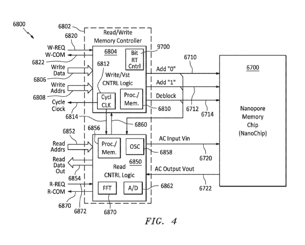
nanopore memory
chip, in accordance with embodiments of the present disclosure.
[010] Figure 5 is a block diagram of a computer system, in accordance with
embodiments of
the present disclosure.
[011] Figure 6 is a block diagram showing a nanopore memory system showing
a read/write
memory controller and an instrument for fluidics/reagents, in accordance with
embodiments of
the present disclosure.
[012] Figure 7 shows three different data format listings of the bits on a
memory string, in
accordance with embodiments of the present disclosure.
[013] Figure 8 shows a data format listing of the bits on a memory string
for each cell in a
row, in accordance with embodiments of the present disclosure.
[014] Figure 9 shows an alternative data format listing of the bits on a
memory string for
each cell in a row, in accordance with embodiments of the present disclosure.
[015] Figure 10 shows an alternative parallel data storage format listing
of the bits on a
memory string for memory cells in a row, in accordance with embodiments of the
present
disclosure.
[016] Figure 11 shows a 4 add-chamber memory cell and an alternative square
geometry top
view, and corresponding two-bit binary codes or DNA bases codes, in accordance
with
embodiments of the present disclosure.
[017] Figure 12 shows a plurality (M) memory cells, each cell having N
addition chambers,
configured to create a Base-N word having M digits, in accordance with
embodiments of the
present disclosure.
[018] Figure 13 is a block diagram of Bit Rate Control Logic, in accordance
with
embodiments of the present disclosure.
[019] Figure 14 is a top-level block diagram of components of a nanopore
polymer memory
system, in accordance with embodiments of the present disclosure.
[020] Figure 15 is a perspective view of an array of cells and an
enlargement of a half a
single cell, in accordance with embodiments of the present disclosure.
2
CA 03111930 2021-03-05
WO 2020/051501 PCT/US2019/050021
[021] Figure 16 shows the illustration of Fig. 15 having loading chambers
disposed below
the array and fluidically connected to deblock chambers of the cells, in
accordance with
embodiments of the present disclosure.
[022] Figure 17 is a perspective view of a memory cell having three micro-
holes in the
bottom of the deblock chamber and having a loading chamber disposed
(detachably or fixedly)
below the deblock chamber, in accordance with embodiments of the present
disclosure.
[023] Figure 18 is a perspective view of an array of memory cells having a
plurality of
micro-holes in the bottom of the deblock chamber and having a loading chamber
disposed below
the deblock chamber, in accordance with embodiments of the present disclosure.
DETAILED DESCRIPTION
[024] The following description of the preferred embodiment(s) is merely
exemplary in nature
and is in no way intended to limit the invention, its application, or uses.
[025] The following commonly-owned pending patent applications contain subject
matter
related to that described herein, each of which are hereby incorporated by
reference in their
entirety to the fullest extent permitted by applicable law: US Patent
Application No. 15/690,189,
filed Aug. 29, 2017; and US Patent Application No. 15/969,745 filed May 2,
2018.
[026] In particular, in some aspects or embodiments, the disclosure provides a
system and
method for storing data on a polymer in a nanopore-based device, comprising
providing a
"memory cell" having at least three chambers, including at least two add
chambers and a
"deblock"/"de-protect" chamber, each of the add chambers having a nanopore
arranged to allow
the polymer to enter and exit the add chamber and each of the add chambers
arranged to add a
unique code to the polymer when the polymer enters the respective add chamber,
and the
"deblock" chamber arranged to enable the polymer to receive the code when the
polymer enters
the respective add chamber; and successively steering the polymer from the
"deblock" chamber
through the nanopore to the add chambers to add the codes to the polymer based
on a
predetermined digital data pattern to create the digital data pattern on the
polymer.
[027] Referring to Fig. 1, a schematic circuit block diagram of a nanopore-
based "memory
chip" 6700, is shown for embodiments of the present disclosure. In particular,
the memory chip
6700 may have a plurality of nanopore-based "memory cells" 6702 (or "storage
cell" or "data
storage cell"), each having the ability to store data. Each of the "memory
cells" 6702 has a multi-
3
CA 03111930 2021-03-05
WO 2020/051501 PCT/US2019/050021
chamber nanopore-based fluidic cell 6704 with a cell structure similar to that
discussed in the
aforementioned patent applications (which are incorporated by reference)
(e.g., having a
membrane with a nanopore and a "memory string" 6550 (e.g., DNA or other
polymer, as
discussed in the aforementioned patent applications). The "memory cells" 6702
may also include
any solid-state or semiconductor passive or active circuitry or chip layers or
components, which
interface with the fluidic cell portion 6704 to provide the data storage (or
writing or adding)
and/or data retrieval (or reading or sequencing) functions described herein.
[028] Referring to Figs. 2 and 3, the memory cells 6702 may be connected
together (electrically
and fluidically), such as 3-chamber memory cells having common fluidic "Add"
channels and
common "Add" electrodes, and independent "deblock" chambers, such as is shown
in Fig. 2, and
described in the aforementioned patent applications. Any number of chambers
and any cell
configurations described herein may be used if desired. In some embodiments,
the memory cell
may be configured as shown in Fig. 3, which is described in the aforementioned
patent
applications regarding Fig. 65 thereof.
[029] In particular, for example, referring to Fig. 2, a partial
perspective drawing having
selective transparent surfaces of a grouping of 3-chamber nanopore-based cells
6500 (each cell
similar to that discussed herein above), of nanopore memory chip is shown for
some
embodiments of the present disclosure. In particular, a group of four 3-
chamber cells
6506,6508,6510,6512 are connected together, such that the upper (or top) left
chambers 6502
(Add "0" chambers) of each of the connected cells 6506-6512 are fluidically
connected together
to form an Add "0" flow channel or Add "0" chambers 6502. In addition, the
upper (or top) right
chambers 6504 (Add "1" chambers) of each of the connected cells 6506-6512 are
also fluidically
connected together to form a separate Add "1" flow channel or Add "1" chambers
6504. In
addition, the Add "0" chambers (or channel) 6502 have a common electrode 6520,
and the Add
"1" chambers (or channel) 6504 have a different common electrode 6522. In some
embodiments
there may be a single metallic or conductive strip providing the common
electrode for each add
channel, and in some embodiments there may be separate electrodes, which are
connected by in-
chip wiring.
[030] Also, any of the embodiments and cell designs disclosed herein may be
used with a
longitudinal resonator design(s) (LNPR) and/or a transverse resonator
design(s) (TNPR)
described in detail in the aforementioned patent applications, for measurement
or reading
4
CA 03111930 2021-03-05
WO 2020/051501 PCT/US2019/050021
molecules structures or data. In particular, transverse resonator design(s)
(TNPR), transverse
electrodes 6590 may be disposed around one or more of the nanopores 6528.
Also, the hardware
and software logic and control logics and embodiments shown herein may also be
used with the
LNPR and/or TNPR configurations.
[031] Below the collective Add channels 6502,6504, are individual "deblock"
chambers
6530-6536, similar to that discussed herein above, that are both fluidically
and electrically
isolated from the other chambers. On the bottom of each of the deblock
chambers 6530-6536 are
corresponding individually controllable "deblock" electrodes, e.g., deblock
electrodes 6514,6516
visible in Fig. 65 correspond to deblock chambers 6534,6536, respectively.
Also, the upper
chambers for the cells 6506-6512 each have a corresponding nanopore 6528
through a
membrane 6529. Also, in this example, the fluidic cell 6512 has a left top Add
"0" chamber 6537
and a right top Add "1" chamber 6539. While the Add "0" chambers for the
fluidic cells 6502-
6512 are fluidically connected via the fluidic channels 6502, and the Add "1"
chambers for the
fluidic cells 6502-6512 are fluidically connected via the fluidic channels
6504, each of the fluidic
cells 6506-6512 has an independent memory storage string (e.g., DNA or
polymer) 6550, which
has one end that traverses through the nanopore 6550 to enter the Add "1" or
Add "0" chambers,
and returns to its corresponding deblock chamber 6530-6536, which is
fluidically and electrically
isolated from the other chambers (in this example). Thus, each of the 3-
chamber fluidic cells
6506-6512 represents an independent memory storage cell, or memory cell
(discussed more
hereinafter).
[032] As the configuration of Fig. 65 has all the Add "0" electrodes
connected together and,
separately, all the Add "1" electrodes connected together, and the deblock
electrodes are
individually controlled, the writing (or adding) may occur in write (or add)
"cycles," such as an
Add "0" cycle, when all the cells that need to write a "0" may be written at
the same time,
followed by an Add "1" cycle, when all the cells that need to write a "1" may
all be written at the
same time. Other data writing cycles or approaches may be used if desired.
[033] In addition, the Add "0" and Add "1" channels 6502, 6504, may be
filled with fluid
(or flushed, or washed or emptied) from the front or back, as shown by the
arrows 6503-6505,
respectively, and the deblock chambers 6530-6536 may be filled with fluid (or
flushed, or
washed or emptied) from the side, as shown by the arrows 6540-6546,
respectively. It is not
required that every Add "1" chamber be fluidically and electrically connected
or that every Add
CA 03111930 2021-03-05
WO 2020/051501 PCT/US2019/050021
"0" chamber be fluidically and electrically connected. If a large number of
them are so connected
it provides efficiencies; in general, the more cells that are connected the
more efficiencies that
can be realized.
[034] Also, the entire polymer (or DNA) or "string" or memory string 6550
may be
prevented from completely exiting the central deblock chamber by binding (or
tethering or
attaching) one end of the polymer 6550 to the surface of the central deblock
chamber 6536, e.g.,
shown as point 6552 in deblock chamber 6536. Other locations in deblock
chamber 6536 may be
used to tether the polymer provided it meets the desired functional and
performance
requirements. In some embodiments, a structure 6554, e.g., a bead, particle,
or origami, or other
structure, may be attached to one end of the polymer 6550 and prevent the
polymer from leaving
the deblock chamber 6536 through the nanopore 6550. Similar criteria apply for
the polymer
memory string 6550 in the other deblock chambers 6530-6534.
[035] The polymer 6550 used to store the data may be DNA as discussed
herein, or it may
be any other polymer or other material that has the properties described
herein. The polymer
6550 used to store data may also be referred to herein as a "memory polymer"
or "memory
string" (due to its string-like appearance).
[036] Referring to Fig. 3, a partial perspective drawing having selective
transparent surfaces
of a grouping of 3-chamber nanopore-based cells 6600 (each cell similar to
that discussed herein
above), of nanopore memory chip is shown for some embodiments of the present
disclosure. In
particular, similar to Fig. 65, a group of four 3-chamber cells
6606,6608,6610,6612 are
connected together, such that the upper (or top) left chambers 6602 (Add "0"
chambers) of each
of the connected cells 6606-6612 are fluidically connected together to form an
Add "0" flow
channel 6602. In addition, the upper (or top) right chambers 6604 (Add "1"
chambers) of each of
the connected cells 6606-6612 are also fluidically connected together to form
a separate Add "1"
flow channel 6604. However, in this embodiment, the Add "0" chambers
associated with the
cells 6606-6612 have separate electrodes 6620-6626, and the Add "1" chambers
associated with
the cells 6606-6612 also have separate electrodes 6630-6636. This fluidic and
electrode
arrangement is similar to that described and shown herein above with Fig. 27.
In some
embodiments, the upper chambers (Add "0" and Add "1") may be fluidically
separated or
isolated from each other to avoid potential electrical-cross talk between
adjacent Add chambers
when trying to control the path of the DNA.
6
CA 03111930 2021-03-05
WO 2020/051501 PCT/US2019/050021
[037] Also, for Fig. 2, deblock chambers may be fluidically connected even
though the
electrodes are separately controlled. In that case, there may be cross-talk
between the channels,
e.g., nearby DNA gets attracted by electric fields and/or current flow seen by
adjacent cells.
[038] In some embodiments, the electrodes may be have 3D shapes, such as a
triangle or
pyramid rising up from the bottom of the cell or protruding down into the
cell. In that case, the
electrode may be constructed to produce a more targeted, focused or closer
electric field to the
nanopore for that cell, which may reduce cross talk between adjacent cells
that are fluidically
connected but electrically separated.
[039] If the memory string (or DNA or polymer) gets so long it may wrap
around from one
add chamber and though the top of another. To avoid that issue, there may be
partial walls
disposed between adjacent cells along the flow channel, to make the distance
between adjacent
nanopores that much longer for long DNA.
[040] Below the Add chambers is a common "deblock" chamber 6640, which is
common to
all the upper Add chambers, similar to that discussed herein above. On the
bottom of the
common deblock chamber 6540 is a common deblock electrode 6642. Also, the
upper chambers
for the cells 6606-6612 may each have the nanopore 6528, similar to that
discussed herein above,
through the membrane 6529.
[041] In addition, the deblock chamber 6540 may be filled with fluid from a
side (depending
on the structural configuration of the cell). In some embodiments, it may be
filled from the left
(or right side), as shown by the arrow 6650. In other embodiments, it may be
filled from the
front (or back) side, as shown by the arrow 6652.
[042] Also, the entire DNA or polymer "string" (or memory string) 6550 may be
kept from
completely exiting the central deblock chamber by binding (or tethering) one
end of the polymer
6550 to the surface of the central deblock chamber 6640, e.g., shown as point
6552 for the cell
6612. A similar arrangement would apply for the other cells 6606-6610. Other
locations may be
used to tether the polymer provided it meets the desired functional and
performance
requirements.
[043] Referring to Fig. 1, the "memory cells" 6702 may be configured as an
MxN array of
memory cells, with M rows and N columns, each of the cells 6702 being labeled
Cm,N. More
specifically, the cells 6702 in the first row are labeled C1,1-C1,N, and the
cells 6702 in the last
row are labeled Cm J-Cm,N. M and N may be any values that provide the desired
functions and
7
CA 03111930 2021-03-05
WO 2020/051501 PCT/US2019/050021
performance, and M,N may each be as small a 1 and as large as 1 million, 10
million, 100
million, 1 billion, or 1 trillion, or larger, depending on the desired
footprint size of the memory
chip and the size of each memory cell.
[044] The memory chip 6700 has an Add "0" input DC voltage on line 6710,
which is
electrically connected (directly or through on-chip circuitry or components,
as described herein)
to each of the Add "0" electrodes. The Add "0" input DC voltage on the line
6710 drives the Add
"0" electrode to the desired voltage state (discussed herein), to help
position (or move or steer)
the memory string 6550 (DNA or other polymer, as discussed herein) to the
desired chamber of
the fluidic cell 6704. In this configuration, all the Add "0" electrodes for
each of the memory
cells are shared or common, or electrically connected, as shown in Fig. 2.
[045] The memory chip 6700 also has an Add "1" input DC voltage on line
6712 which is
electrically connected (directly or through on-chip circuitry or components as
described herein)
to each of the Add "1" electrodes. The Add "1" input DC voltage on the line
6710 drives the Add
"1" electrode to the desired voltage state (discussed herein), to help
position (or move or steer)
the memory string 6550 (DNA or other polymer, as discussed herein) to the
desired chamber of
the fluidic cell 6704. In this configuration, all the Add "1" electrodes 6522
for each of the
memory cells is shared or common, as shown in Fig. 2.
[046] The memory chip 6700 also has a "Deblock" input DC voltage on a
plurality of lines
(or bus) 6714, each of which is electrically connected (directly or through on-
chip circuitry or
components as described herein) to a corresponding "deblock" electrode in each
of the cells
6702. The deblock input DC voltage drives the corresponding deblock electrode
for a given cell
to the desired voltage state (discussed herein), to help position (or move or
steer) the memory
string 6550 (DNA or other polymer, as discussed herein) to the desired chamber
of the fluidic
cell 6704. In this configuration, each of the deblock electrodes are
independently driven, as
shown in Fig. 2, thus the need for the deblock plurality of electrical
connections or bus (or
deblock bus) 6714. Each row of memory cells 6702 will have a corresponding
number of
deblock input DC voltage lines provided. For example, the first row there is a
set of N deblock
lines 6716 feeding the N cells 6702 in that row, and in the last row M, there
is a separate set of N
deblock lines 6718 feeding the N cells 6702 in the row M.
[047] The DC input voltages Add "0", Add "1", and deblock, on the lines
6710, 6712, 6714,
respectively, may be referred to herein as DC "steering" voltages VST (or
polymer or DNA
8
CA 03111930 2021-03-05
WO 2020/051501 PCT/US2019/050021
steering voltages or memory string steering voltages) as they are used to
"steer" the polymer
memory string to the appropriate chamber of the fluidic cell 6704 at the
appropriate time to
achieve the desired result, e.g., write or add a "0" or "1" onto the memory
string, or do nothing,
or move the memory string to a particular chamber to enable writing or reading
data, or perform
validation testing, or the like. DC input voltages Add "0", Add "1", and
deblock, on the lines
6710, 6712, 6714, respectively, may be provided from a computer-based
controller circuit or
logic or device, as described herein, which has the appropriate logic to
perform the functions
described herein.
[048] The memory chip 6700 also has an AC input voltage Vin, and an AC
output voltage
Vout, on line 6720, 6722, respectively. The AC input voltage Vin on the line
6720 is electrically
connected, as described herein, to each of the memory cells 6702 in parallel.
The AC Vin
provides an AC signal, e.g., rf or radio frequency signal, on the line 6720 to
each of the memory
cells 6702 and the memory cells are configured to be a resonator or nanopore
polymer resonator
(NPR), each having a different frequency response to the input AC Vin, as
discussed in the
aforementioned patent applications. The line 6720 may connect the memory cell
6702 and/or the
electronic components on the chip, the electrodes, and the fluidic cell 6704
therein, differently
from that shown in Fig. 1, depending on the circuit configuration used for the
nanopore polymer
resonator (NPR), fluidic cell configuration, electrode configuration, or other
factors, as described
herein. The AC input voltage Vin on the line 6720 may be provided from a
computer-based
controller circuit or logic or device, as described herein, which has the
appropriate logic to
provide the appropriate AC input voltage Vin and perform the functions
described in the
aforementioned patent applications.
[049] The combined frequency response from each of the memory cell 6702 may
be
provided to an on-chip amplifier (or pre-amp) 5320 (as described in the
aforementioned patent
applications with regard to Fig. 53 therein), which provides the AC output
voltage Vout on the
line 6722 indicative of the combined frequency response. The AC output voltage
Vout on the
line 6722 may be provided to a computer-based processing circuit or logic or
device, which has
the appropriate logic, e.g., analog-to-digital (A/D) conversion and digital
signal processing
(DSP) logic, as described herein, which reads the data stored on the memory
string 6550 and
may perform other functions as described in the aforementioned patent
applications. Other
9
CA 03111930 2021-03-05
WO 2020/051501 PCT/US2019/050021
reading techniques may be used if desired, such as dc bias current
measurement, as described in
the aforementioned patent applications.
[050] In some embodiments, the nanochips can be fabricated for example as
depicted in Figures
23-29 in the aforementioned patent applications. For example, in one format,
each polymer
strand is associated with two or four addition chambers, wherein the two
addition chamber
format is useful for encoding binary code in the polymer, and the four
addition chamber format
is particularly useful for making custom DNA sequences. Each addition chamber
contains a
separately controllable electrode. The addition chambers contain reagents to
add monomers to
the polymer in buffer. The addition chambers are separated by a membrane
comprising one or
more nanopores from a reserve chamber, which may be common to multiple
addition chambers,
and which contains deprotection reagents and buffer, to deprotect the
protected monomers or
oligomers added in the addition chambers. The nanochips comprise a
multiplicity of addition
chamber sets, to allow parallel synthesis of many polymers.
[051] In some embodiments, the present disclosure provides a method for
storing and reading
data on a polymer in situ in a nanopore-based chip, comprising: providing a
cell having at least
three chambers, including an Add "1" chamber arranged to add a "1" bit to the
polymer and an
Add "0" chamber arranged to add a "0" bit to the polymer, and a "deblock"
chamber arranged to
enable the polymer to receive the "1" bit and "0" bit when the polymer enters
the Add "1" or
Add "0" chambers, respectively; successively steering the polymer from the
"deblock" chamber
through the nanopore to the Add "1" chamber or to the Add "0" chamber based on
a
predetermined digital data pattern to create the digital data pattern on the
polymer; and reading
the digital data stored on the polymer as it passes through the nanopore using
a resonance
frequency response of a nanopore-polymer resonator (NPR) on the chip, or a dc
bias current
change or other detection technique, which are described in the aforementioned
patent
applications, or any other detection technique.
[052] Referring to Fig. 4, a top level hardware block diagram is shown of a
read/write
memory storage system 6800 having the nanopore-based memory chip 6700 (Fig. 1)
and a
memory read/write controller 6802, in accordance with embodiments of the
present disclosure
and as described in the aforementioned patent applications. In particular, the
memory read/write
controller 6802 may have a write controller logic 6804, which receives input
data to be written to
the memory chip 6700 on lines and an address to store the data (or label or
pointer or the like) on
CA 03111930 2021-03-05
WO 2020/051501 PCT/US2019/050021
lines 6808, and provides the DC steering voltages Add "0", Add "1", and
deblock, on the lines
6710, 6712, 6714, respectively, to the nanopore memory chip 6700. The write
controller 6804
has the appropriate hardware, software and firmware (including any
microprocessor or micro-
computer based processor chips or devices and/or memory storage) as needed to
provide the
functions described herein, as indicated by a Proc./Mem. box 6810.
[053] In addition, the write controller 6804 may also provide a write (or
add) cycle clock
6812 (or oscillator), which determines when the memory chip 6700 writes (or
adds or stores) "0"
or "1" bits. In particular, the write controller chip 6804 provides the DC
steering voltages (Add
"0", Add "1", Deblock) based on the write cycle clock 6812 to cause the memory
chip 6700 to
write "1" or "0" to the memory cells. As discussed herein above with Fig. 2,
in certain cell
configurations, such as when all the Add "0" electrodes are connected together
and, separately,
all the Add "1" electrodes are connected together, and the deblock electrodes
are individually
controlled (such as in Fig. 2), the writing (or adding) of data bits may occur
in write (or add)
"cycles," such as an Add "0" cycle, when all the cells that need to write a
"0" may be written at
the same time, followed by an Add "1" cycle, when all the cells that need to
write a "1" may all
be written at the same time. The write cycle clock provides a write cycle
signal on a line 6814 to
enable the write requesting device or platform or computer bus, to determine
the writing status of
the memory chip. Other data writing cycles, timing, or approaches may be used
if desired.
[054] In some embodiments, the write controller 6804 may also receive
control signals from
the system or computer bus, such as a Write Request (W-REQ) signal on a line
6820 to request
certain data be written to the memory chip 6700, and the write controller 6804
may also provide
a Write (or Add) Complete (W-COM) signal on a line 6822, to indicate when the
requested data
has been written to the memory chip 6700.
[055] The memory read/write controller 6802 may also have memory read
controller logic
6850, which may receive a read address (or label or pointer or the like) on
lines 6852
corresponding to the storage location of the data desired to be read from the
memory chip 6700,
and provides the requested data read from the memory chip 6700, on the lines
6854. The read
controller 6850 may also have the necessary logics and components to provide
the AC input
voltage signal Vin to the memory chip 6700 on the line 6720. The AC input
voltage Vin, as
described herein, is an AC rf (radio frequency) signal that has frequency
components
corresponding to the bandwidth of the nanopore resonators (NPRs) in the memory
chip 6700. To
11
CA 03111930 2021-03-05
WO 2020/051501 PCT/US2019/050021
provide the Vin signal, the read controller 6850 may have a frequency
oscillator logic 6858
(programmable or non-programmable), which provides the necessary frequency
components
(discussed herein) to enable the read controller logic to read the requested
data from the
nanopore memory chip 6700. As discussed herein, the AC Vin signal may be
directly
synthesized, combine multiple probe frequencies, and may be a single broadband
signal, or a
time swept or stepped frequency signal, or any other AC signal the provides
the functions
described herein as described in the aforementioned patent applications.
[056] The read controller 6850 also receives the output AC Vout voltage
from the memory
chip 6700 on the line 6722, and performs AID conversion and digital signal
processing (e.g.,
using on-board AID conversion logic 6862 and FFT (fast Fourier transform)
logic 6864), as
discussed herein or in the aforementioned patent applications, on the Vout
signal to determine
the values of the desired data at the specified read address and provide the
output data on Read
Data Out the lines 6854.
[057] The read controller 6850 has the appropriate hardware, software and
firmware
(including any microprocessor or micro-computer based processor chips or
devices and/or
memory storage) as needed to provide the functions described herein or as
described in the
aforementioned patent applications, as indicated by a Proc./Mem. box 6856.
[058] In addition, the read controller 6850 may also receive the write (or
add) cycle clock
signal on the line 6814 from the write cycle clock 6812 (or oscillator),
which, as discussed
above, determines when the memory chip 6700 will write (or add or store) "0"
or "1" bits. In
particular, controller chip 6804 will provide the DC steering voltages (Add
"0", Add "1",
Deblock) based on the write cycle clock 6812 to cause the memory chip 6700 to
write "1" or "0"
to the memory cells. Because the act of writing with the present disclosure
requires the DNA (or
polymer or memory string) to pass through the nanopore to enter the desired
chamber to Add bits
and also to pass through the nanopore when exiting back to the deblock
chamber, the write cycle
clock signal may also be used by the read controller 6850 to determine when is
the best time to
read the data, as discussed with Fig. 69 in the aforementioned patent
applications.
[059] In some embodiments, the read controller may provide a read signal
6860 to the write
controller 6804 to request the controller 6804 provide the necessary steering
voltages (Add "0",
Add "1", Deblock) on the lines 6710-6714 to cause the memory string 6550 (Fig.
1) to pass
through the nanopore to enable reading of the memory string.
12
CA 03111930 2021-03-05
WO 2020/051501 PCT/US2019/050021
[060] In some embodiments, the read controller 6850 may also receive a Read
Request (RD-
REQ) signal on a line 6870 to request certain data be read from the memory
chip 6700, and the
read controller 6850 may also provide a Read Complete (RD-COM) signal on a
line 6822, to
indicate when the requested data has been read from the memory chip 6700. The
Memory
Controller 6802 may perform only one function, e.g., read or writing to the
nanopore chip if
desired, or it may perform both of these functions (Read and Write), if
desired.
[061] Referring to Fig. 5, the Nanopore memory system 6800 may be part of a
larger
computer system which may interact with an Address/Data/Control Bus 6870, and
may also
interact with separate memory controllers 6876, all of which interact with one
or more
CPU/Processors 6874. For example, one or more of the read/write address and/or
data inputs,
outputs and/or control lines, such as numerals 6820, 6822, 6806, 6808, 6814,
6852, 6854, 6872,
6870, shown in Fig. 4, may be received from or provided to the bus 6872 or the
memory
controller 6876. The computer system 6870 may interface with a user 6878 and a
display screen
6880.
[062] Referring to Fig. 6, the nanopore chip 6700 (Fig. 1) may interact
with the read/write
memory controller 6802, as discussed herein above with Fig. 4, as part of an
overall storage
system 7500, which may control the voltages (AC and DC) to steer or control
the polymer to
Add bits and or read the bits on the memory string as shown collectively by
lines 7504. The
memory chip 6700 may also interface with an instrument 7502 on lines 7506,
which may provide
fluidics to the memory chip, such as filling the chip with buffers, enzymes,
and/or polymers or
DNA (or other memory strings), as discussed herein. The Instrument 7502 and
the Memory
Controller 6802 may be controlled or receive commands from a Computer System
6870, such as
that described and shown with Fig. 5, that may interact with the user 6878 and
may have the
display 6880. The computer system 6870 may interact with the Read/Write Memory
Controller
6802 and the Instrument 7502 via the computer bus 6872 (Fig. 4). The
instrument 7502 has the
necessary electronics, computer processing power, interfaces, memory,
hardware, software,
firmware, logic/state machines, databases, microprocessors, communication
links, displays or
other visual or audio user interfaces, printing devices, and any other
input/output interfaces,
including sufficient fluidic and/or pneumatic control, supply and measurement
capability to
provide the functions or achieve the results described herein.
13
CA 03111930 2021-03-05
WO 2020/051501 PCT/US2019/050021
[063] In particular, the instrument may perform the following fluidic
actions with the
memory chip: initially fill the chip with the necessary fluids, enzymes,
reagents, DNA, or the
like through capillary action & or micro pumping. For the embodiments where
the Addl and
Add have flow-through channels and deblock as isolated chambers, the deblock
chambers could
be filled en-masse (via capillary action) first, then sealed - water and
buffers would travel into
the add chambers which could then be filled with their enzymes/buffers OR
deblock chambers
could be individually filled via targeted addition (e.g., ink-jet) and dried
and sealed. In that case,
the Add chambers may be filled under vacuum to ensure no bubbles get trapped
in the deblock
chamber, or the deblock chambers may be sealed with a material which allows
gas but not water
to pass through (such as PDMS). Also, the deblock chambers may be filled by
leaving the
bottom of the cell open during assembly, and placing the cell bottom in the
desired fluid, and the
fluid will wick up into the deblock chambers by capillary action.
[064] There are various fluidics designs that will achieve the desired
results for fluidic filling
and flushing. For example, the Add "0" channels and Add "1" channels may
respectively be
connected together (like channels together) in a continuous serpentine (back
and forth) pattern,
and fed fluid through vias from a layer above the channels. The vias may
connect to the
instrument via standard fluidic interfaces sufficient to supply the desired
fluids to the channels.
In some embodiments, the Add channels may each be fed through separate vias
from a common
reservoir for Add "0" channels and from a separate common reservoir for Add
"1" channels
located on a layer above the channels. Any other fluidic design may be used if
desired. Sample
dimensions for the Add channels, are: width about 100 nm to about 10 microns,
height of about 1
micron to about 50 microns, and length of about 100 mm (lcm or 1000 microns)
from one side
of the chip to the other. A serpentine connected channel would be a multiple
of this depending on
how many channels are connected in series. The nanopore may have a diameter of
about 2-20
nm, e.g. about 2 to about 10 nm, for example about 2 to about 5 nm. Other
diameters may be
used if desired provided it provides the desired function and performance.
[065] The instrument 7502 may also be used during initialization and cell
testing if desired.
For example, for cell initialization & cell testing Quality Control (QC) for
nanopore quality to
ensure expected current is observed (current proportional to pore size). Also,
QC for DNA
presence: ensure that the expected current (or capacitance or impedance, or
shift in magnitude or
phase of the resonance, as discussed herein) changes characteristic of DNA (or
polymer, etc.)
14
CA 03111930 2021-03-05
WO 2020/051501 PCT/US2019/050021
moving though the nanopore (e.g., expected reduction in current, or shift in
magnitude or phase
of the resonance, as discussed herein). In addition, it may be used for QC for
circuit formation
which would be similar to that performed for nanopore quality.
[066] The instrument 7502 may also be used for DNA addition, as previously
described
herein, where DNA with origami is introduced via one of the add chambers (or
channels),
current may be applied to cells until insertion is detected, modified DNA end
in deblock chamber
diffuses and then attaches to surface, and restriction enzyme introduced to
add chamber to cleave
origami which is then removed via buffer flow. For example, the present
disclosure provides
DNA synthesis wherein the DNA is single or double stranded, at least 1000
nucleotides long,
e.g., 1000 ¨ 1,000,000 nucleotides or, for example, 5,000 to 20,000
nucleotides long, wherein the
sequence of the nucleotides corresponds to a binary code. Other DNA lengths
may be used if
desired.
[067] Also, the present disclosure provides for DNA (or polymer) wherein
the nucleotides in
a single strand or in the coding strand are selected from adenine, thymine and
cytosine
nucleotides, e.g., are selected from adenine and cytosine nucleotides or
thymine and cytosine
nucleotides. Also, the DNA may consist primarily of nonhybridizing
nucleotides, so that it will
not form significant secondary structures when in the form of a single strand.
Also, it provides
DNA wherein the nucleotides are at least 95%, e.g., 99%, e.g., 100% adenine
and cytosine
nucleotides. Also, the present disclosure provides DNA comprising a nucleotide
or sequence of
nucleotides added to separate or punctuate the nucleotides comprising a binary
code, e.g., to
separate the l's and O's or groups of l's and O's, so that consecutive l's or
0's can be more
easily read. The present disclosure also provides DNA wherein (a) each bit in
the binary code
corresponds to a single nucleotide, e.g. each of 1 and 0 correspond to A or C;
or (b) each bit in
the binary code corresponds to a series of more than 1 nucleotides, e.g. 2, 3
or 4 nucleotides, e.g.,
AAA or CCC. In addition DNA may be crystallized, or provided in a dry form
together with one
or more of a buffer salt (e.g., a borate buffer), an antioxidant, a humectant,
e.g. a polyol, and
optionally a chelator, for example as described in US 8283165 B2, incorporated
herein by
reference; and/or in a matrix between the nucleic acid and a polymer, such as
poly(ethylene
glycol)¨poly(1-lysine) (PEG¨PLL) AB type block copolymer; and/or together with
a
complementary nucleic acid strand or a protein that binds the DNA.
CA 03111930 2021-03-05
WO 2020/051501 PCT/US2019/050021
[068] Also, the DNA (or polymer) may contain an identifying sequence, or DNA
that contains
PCR amplification sequences, or the DNA may contain one or more calibrating
sequences, e.g.,
known sequences of nucleotides which can be used to calibrate a nanopore-based
sequencing
device, e.g. to measure the speed of the DNA passage through the nanopore or
the relative effect
on capacitance or current attributable to different nucleotides passing
through the nanopore.
Also, the DNA may contain a terminal linker group enabling it to be anchored
to a surface near
the nanopore in a nanopore-based device, a spacer sequence long enough to
permit the DNA
strand to reach the nanopore when anchored to a surface, a data storage
sequence wherein the
sequence encodes data, codons or other information, and optionally a
restriction sequence,
enabling the DNA to be cleaved and retrieved once synthesized.
[069] Referring to Fig. 7, the format of how data is stored may vary based
on various factors
and design criteria. In particular, the "memory string" (or DNA or polymer)
6550 may be shown
as a line 7102 on which are a series of ovals 7104, indicative of individual
"bits" written (or
added) onto the memory string 6550 in a given memory cell. In some
embodiments, the bits
7104 may be written one after the other to build a "storage word" 7112. A
first example data
format 7110 shows three components to the storage word 7112, an address
section 7106, a data
section 7108, and an error checking section 7110. The address section 7106 is
a label or pointer
used by the memory system to locate the desired data. Unlike traditional
semiconductor memory
storage where hardware address lines on a computer memory bus would address a
unique
memory location, the memory chip and system of the present disclosure require
the address (or
label) to be part of the data stored and indicative of where the data desired
to be retrieved is
located. In the examples shown in Fig. 7, the address is located proximate to
or contiguous with
the data, as well as error checking data, such as parity, checksum, error
correction code (ECC),
cyclic redundancy check (CRC), or any other form of error checking and/or
security information,
including encryption information. In the storage word 7112, each of the
components Address
7106, Data 7108, Error Checking 7110, are located after each other in the
memory string. As
each of the components have a known length (number of bits), e.g., address =
32 bits, data = 16
bits, error check = 8 bits, each storage word 7112 and its components can be
determined by
counting the number of bits.
[070] Another example data format 7120 shows the same three components,
address section
7106, data section 7108, and error checking section 7110. However, in between
each of the
16
CA 03111930 2021-03-05
WO 2020/051501 PCT/US2019/050021
sections there is a "special bit(s) or sequence" sections Sl,S2,S3, shown as
numerals
7122,7124,7126, respectively. These special bits Sl,S2,S3 may be a
predetermined series of bits
or code that indicate what section is coming next, e.g., 1001001001 may
indicate the address is
coming next, whereas 10101010 may indicate the data is coming next, and
1100110011 may
indicate the error checking section in next. In some embodiments, the special
bits may be a
different molecular bit or bit structure attached to the string, such as
dumbbell, flower, or other
"large" molecular structure that is easily definable when it passes through
the nanopore. Instead
of it being large it may have other molecular properties that provide a unique
change the
capacitance or resonance different from the 1 bits and 0 bits, as discussed
herein above.
[071] Another example data format 7130 shows only Data components 7140 with
no address
component, and an error checking component 7110. In this structure, the string
holds only the
"Data" components and no Address components, which may be stored in other
strings, as
discussed hereafter. In this example there are also Special bits S1,S2,S3,
shown as numerals
7132,7134,7136, respectively. Similar to the example 7120, these special bits
S1,S2,S3 may be a
predetermined series of bits or code that indicate the separation between data
sections (e.g., the
beginning or end of a data string or data section) and indicate when an error
checking section is
next, or may be a different molecular bit or bit structure attached to the
string that is easily
definable (or identifiable) when it passes through the nanopore, as discussed
herein above.
[072] Referring to Fig. 8, a single row of memory cells 7202-7208 (Celli to
CellN) is
shown, with a sample memory string 7210-7216, respectively, associated with
each cell. The
memory system of the present disclosure is significantly different from
traditional semiconductor
memory because instead of each memory cell storing a single bit of information
(1 or 0), each
memory cell of the present disclosure can store a significant amount of data
(i.e., a "string" of
data or "data string" or "memory string"). Thus, if a traditional
semiconductor memory is viewed
as a 2D array, the present memory system may be viewed as a 3D array, where
each memory cell
location in the memory cell array has significant storage depth. This provides
a large range of
options for how to store data and retrieve data.
[073] For the example shown in Fig. 8, each cell may store a linear self-
contained string of
information (storage word), similar to that discussed in the example 7110 of
Fig. 7. In that case,
each storage word is stored back-to-back on top of (or sequentially with)
other storage words
17
CA 03111930 2021-03-05
WO 2020/051501 PCT/US2019/050021
along the memory string. And each of the cells 7202-7208 in the row replicates
this structure,
and this may be repeated for multiple rows (not shown).
[074] Referring to Fig. 9, in some embodiments, some cells may store only
address
information, and some cells only data information. In that case, each row may
have a cell, e.g.,
Cell 1, 7310, which has a memory string 7302 of addresses or pointers, and the
remainder of the
rows, e.g., Ce112-CellN, 7310-7316, respectively, have corresponding strings
of data 7304-7308,
respectively. In that case, the addresses or pointers would have a value
indicative of where the
data is stored on the memory chip, such as a row, column and entry number,
e.g. Row 3, Column
8, Entry 50, meaning the data corresponding to this address resides at the
50th data block on the
memory string, located in Row 3 and Column 8. This effectively decouples the
address from
being located physically next to the data, which can provide flexibility in
storage. Also, each of
the strings may have one or more error checking or security components to
validate the
information stored on the string. This may be repeated for each row in the
array.
[075] Referring to Fig. 10, instead of storing information contiguously (or
serially) on a
given memory string, the data may be stored in the memory cell array in
parallel (e.g., across a
plurality of memory strings). For example, when a storage word is stored, it
may be able to be
stored more quickly in a single storage action, storing it across the array,
similar to the way
traditional semiconductor memory works, but allowing it to do it over and over
again due to the
3D depth, each time "pushing" (storing) another storage word in parallel onto
a predetermined
group of memory strings. Such a format also enables quick parallel retrieval
of a given storage
word (once located). In that case, certain cells 7402 may be allocated to
storing addresses/
pointers in parallel, certain cells 7204 may be allocated to storing data in
parallel, and certain
cells 7406 may be allocated to storing error checking and security data in
parallel. For example,
the storage word ("Address, Data, Error Checking") stored on memory string
7210 shown in Fig.
8 (which is stored in series on the one string 7210), may be stored as shown
as storage word
7410, having Addressl, Datal, and Error Checkl, and which is stored in
parallel across a
plurality of cells (1-N, N+1 to M, and M+1 to P). Similarly, for storage word
7412 which would
be stacked across the same strings in parallel with the storage word 7410
(either underneath or on
top of, depending on the direction of storage on the string). In some
embodiments, the data may
be stored in parallel in 2 Dimensions (e.g., across a 2D array or matrix of
rows and columns at a
given layer or depth level), thereby creating a layered 2D array of stored
information, such as a
18
CA 03111930 2021-03-05
WO 2020/051501 PCT/US2019/050021
multi-layered 2D image capture data may be stored, except allowing a 2D image
it to be stored
simultaneously at one time, in realtime, with each 2D snapshot stored in the
cell array in a single
layer on top of the prior snap shot image in the array.
[076] As also discussed in the aforementioned patent applications, while DNA
using two and
four bits (or bases) representing data to be read have been described herein,
any number of "bits"
(or monomers or bases) may be used if desired for the data storage polymer (or
memory string),
provided the change in cell capacitance or impedance (and corresponding
resonance frequency,
or frequency response) is sufficient to produce an output magnitude and/or
phase for each bit that
is distinguishable over each of the other bits. While such capacitance (or
impedance) change may
be accomplished by changing the physical molecular size of the bases (e.g.,
the diameter), any
property of the bases that creates a unique capacitance (or impedance) value
of the cell when
passing through the nanopore may be used if desired. For example, bases that
have different
dielectric properties, different ionic (or charge) properties, and/or
different quantum
mechanical/electrical properties, may be used, provided they meet the desired
functional and
performance requirements.
[077] As also discussed in the aforementioned patent applications, the bits
may be binary bits;
however, they are not limited to any base numbering system as the present
disclosure allows the
memory (or polymer) string (or strand or stick) to write (or add) more than
two different values,
as described herein. In that case, the cell design would be adjusted
accordingly. For example, for
a base-4 system (e.g., GCAT, for DNA based system), there would be 4 add
chambers and a
single de-block chamber, as described herein. This can be extended for any
base number system
greater than 2, such as 3,4,5,6,7,8,9,10 (decimal), or more, up to N. Where
there would be N add
chambers and 1 deblock chamber. The only limitation would be that the chambers
are oriented
such that the memory string (or DNA or polymer) can reach all the add
chambers, as discussed
more herein with Figs. 11-12.
[078] As also discussed in the aforementioned patent applications, Figure 26
in the
aforementioned patent applications also depicts a top view showing four
addition chambers
which share a common reserve or deblock chamber and the polymer is tethered at
a position (9)
with access to each of the four chambers. The cross section (side view) of
this layout would be
as depicted in Figures 24 and 25 in the aforementioned patent applications,
and the charged
19
CA 03111930 2021-03-05
WO 2020/051501 PCT/US2019/050021
polymer can be moved into each of the four addition chambers by operation of
the electrodes in
the electrical control layer (1 in Figure 24 in the aforementioned patent
applications).
[079] More specifically, referring to Fig. 11, two 4 add-chamber memory
cells are shown, a
side view of a row of chambers, and a top view of a square geometry
configuration of chambers.
In both configurations. the memory string 6550 resides in a deblock (DB)
chamber and can enter
the four addition or "add" chambers. Each of the four add chambers has a
unique chemical
construct (or monomer) or code that is added to the polymer memory string
6550. This can be
viewed as four (4) unique codes, which in binary would be 00, 01, 10, 11 (or 0
to 3 in decimal).
The four codes could also be the four bases in DNA, i.e., GCAT, as discussed
herein and in the
aforementioned patent applications. Such a configuration enables the bulk
writing of information
or data (multiple bit writing) with a single chamber add reaction, which
increases the storage
density of data and speed at which the data can be stored, over writing a
single bit during each
write cycle (or add reaction). This can be done for any number of unique
addition chambers that
provide a unique code (or chemical item or construct) in a given memory cell,
the only limit is
the number of unique chemical items or constructs that can be added or written
to the memory
string (or polymer), and that can be identified (or read), as described more
herein.
[080] In particular, Fig. 11 shows 4 Add-Chambers in Memory Cell; 2-bit
binary writing (00
to 11) OR Any set of 4 different (unique) codes or chemical items (e.g.,
G,C,A,T (DNA bases),
or flowers, stars, dumbbells, etc.). Some other features include: DNA (or
other polymer
"memory string") attached to a bead or origami or to bottom (or a wall) of de-
block (DB)
chamber (if long enough); enables bulk writing of information/data, e.g.,
codes or multiple bit
writing, with a single add-chamber reaction; can be done for any number of
unique add chambers
in a given memory cell; and limited only by the number of unique chemical
items or constructs
(or monomers) that can be added or written to the memory string and that can
be identified
(read).
[081] Referring to Fig. 12, in some embodiments, using various multi-bit
writing
configurations, such as those shown and described in the aforementioned patent
application (or
any other configurations that accomplish the same result), may be used to
create an array or
plurality of N-chamber memory cells to provide further enhanced data storage
density. In
particular, M memory cells having N add chambers per cell, allows for the
creation of a Base-N
storage "word" having M digits, written in parallel across memory strings for
each of the cells,
CA 03111930 2021-03-05
WO 2020/051501 PCT/US2019/050021
where the "word" would have values of 0 to (NAM)-1. Also, a single memory cell
or string
creates a Base-N "word" having M digits or codes along the length of the
memory string (word
values of 0 to (NAM)-1), written in a single memory cell or string.
[082] Also, in that case, the cells (Ce111-CellM) may, in some embodiments,
all be identical,
each cell having the same N unique codes. Fig. 12 shows examples for several
different values of
N (number of unique add chambers per cell). In particular, for N=4, each cell
would have four
unique values or states capable of being stored in each corresponding memory
string (each cell
being similar to that shown in Fig. 11). Similarly, for N=8, each cell would
have eight unique
values or states capable of being stored in each corresponding memory string.
Similarly, for
N=10, each cell would have ten unique values or states (or decimal) capable of
being stored in
each corresponding memory string. Similarly, for N=16, each cell would have
sixteen unique
values or states (or hexadecimal) capable of being stored in each
corresponding memory string.
Also, each of the bit writing configurations and approaches discussed herein
with Figs. 7-10,
may be done using multi-bit memory cells (more than 2 add chambers) instead of
single "bit"
cells. In that case, each "bit" oval 7104 (Fig. 7) along the memory string
7102, may represent a
plurality of bits or unique code, corresponding to the number of add chambers
having unique
chemical constructs in the memory cell being used. As a result, high density
data storage is
achieved using such the multi-bit writing approach of the present disclosure.
[083] Also, Fig. 12 shows: M memory cells with N add chambers per cell (and
one De-
Block chamber (DB) per cell); the N add chambers correspond to N different (or
unique) adding
states or chemical constructs; each cell (or corresponding memory string) can
be used to create a
Base-N "digit" (or bit or byte); group of M cells creates a Base-N "word"
having M digits (word
values of 0 to (NAM)-1), written in parallel across multiple memory cells or
strings. Also, a
single memory cell or string creates a Base-N "word" having M digits or codes
along the length
of the memory string (word values of 0 to (NAM)-1), written in a single memory
cell or string.
[084] In some aspects or embodiments, the invention provides a method for
storing data on a
polymer in a nanopore-based device, comprising providing a memory cell having
at least three
chambers, including at least two add chambers and a "deblock"/"de-protect"
chamber, each of
the add chambers having a nanopore arranged to allow the polymer to enter and
exit the add
chamber and each of the add chambers arranged to add a unique code to the
polymer when the
polymer enters the respective add chamber, and the "deblock" chamber arranged
to enable the
21
CA 03111930 2021-03-05
WO 2020/051501 PCT/US2019/050021
polymer to receive the code when the polymer enters the respective add
chamber; and
successively steering the polymer from the "deblock" chamber through the
nanopore to the add
chambers to add the codes to the polymer based on a predetermined digital data
pattern to create
the digital data pattern on the polymer.
[085] In some aspects or embodiments, the invention provides a method for
storing data
using a polymer, comprising: providing a nanopore polymer memory device, the
device having
at least one memory cell comprising at least two addition chambers, each of
the addition
chambers arranged to add a unique code to the polymer when the polymer enters
the respective
addition chamber, the data comprising a series of the codes having a number of
data states
corresponding to the number of unique codes; and successively steering the
polymer through the
nanopore into the addition chambers to add the codes to the polymer based on a
predetermined
digital data pattern to create the digital data pattern on the polymer.
[086] In some embodiments, the number of unique codes for each memory cell
may be any
integer greater than 2. In some embodiments, the number of unique codes for
each memory cell
may a binary number. In some embodiments, the number of unique codes for each
memory cell
may be a binary number greater than 2, such as: 4, 8, 16, 32, 64, 128, 256,
512, 1024, 2048,
4096, 8192, 16384, 32768, or 65536, or higher. In some embodiments, each code
may be
indicative of a digit in a word, the digit having a Base-N based on the number
of unique codes,
and the word having a length M based on the number of digits. In some
embodiments, the code is
indicative of a multi-bit binary digital code.
[087] Also, in some embodiments, each code may be indicative of a digit in
a word, the digit
having a Base-N based on the number of unique codes, and the word having a
length M based on
the number of digits. In some embodiments, the nanopore memory device of the
present
disclosure may include one or more memory cells in the device. Also, any
technique for reading
the unique codes written to the memory string (or polymer) may be used if
desired.
[088] In the case where more than two add chambers are used for a memory
cell, the cells
shown in Fig. 1 would be replaced with cells having more than two add
chambers. In that case,
the corresponding input and output voltage control lines would change as
appropriate to
accommodate the additional add chambers. In that case, the number of
resonators or resonant
frequencies may increase as appropriate, depending on the resonator design
configuration used,
as would be understood by those skilled in the art. A corresponding change may
be made, as
22
CA 03111930 2021-03-05
WO 2020/051501 PCT/US2019/050021
appropriate, to any of the embodiments discussed herein (or in the
aforementioned patent
applications) when increasing the number of add chambers above two, as would
be understood
by those skilled in the art.
[089] The term "data" as used herein includes all forms of data including
data representing
addresses (or labels or pointers, including physical or virtual), machine code
of any type
(including but not limited to object code, executable code and the like),
error checking,
encryption, libraries, databases, stacks, and the like that may be stored in
memory. In certain
examples, such as in Figs. 7-10 (or elsewhere as the context implies), the
term "Data" may be
shown or described as being separate from the "Address," or "Error Checking".
In those cases,
these terms may be used to show different forms of data for illustrative
purposes only.
[090] As discussed hereinbefore, when the DNA (or polymer) memory string is
passing
through the nanopore, the DNA translocation rate (or transfer rate, or
velocity) may vary based
on numerous factors, including, but not limited to, the applied electric
field, the angle of the
DNA string approaching the nanopore, the geometry of the nanopore (cone,
cylinder, etc.), the
diameter of the nanopore compared to the diameter of the string (which may
vary along its
length), the amount of tangling or wrapping or coils in the string, how the
velocity varies along
the length of the string, fluid dynamic effects, friction/attraction/binding
with walls of chamber,
viscosity effects, acoustic waves in the fluid, and other factors.
Accordingly, it would be
desirable to have a consistent predetermined translocation rate, which
corresponds to data bit
rate, to provide the ability to read the data stored in the DNA (or polymer)
memory string
accurately, repeatably and reliably.
[091] As also discussed herein, the DC steering voltage Vst (or Vin) may be
applied to the top
and bottom electrodes to move or steer the DNA from one fluid-filled chamber
to another
through the nanopores. As also discussed, the DNA translocation time (or rate
or speed or
velocity) of the DNA through the nanopore may be adjusted or stopped at any
time by adjusting
the magnitude and polarity of the DC component of the Vst, while not affecting
the AC
measurement or sensitivity.
[092] Referring to Fig. 13, a Bit Rate Control (BRC) Logic 9700 may be used to
provide a
closed-loop feedback control system or servo controller to adjust or drive the
DNA steering
voltage Vst (and thus the translocation rate of the DNA) to obtain a desired
consistent data bit
rate, in accordance with embodiments of the present disclosure. In some
embodiments, the BRC
23
CA 03111930 2021-03-05
WO 2020/051501 PCT/US2019/050021
Logic 9700 may be part of the Read/Write Memory Controller 6802 (Fig. 4)
and/or may be part
of the Write/Vst Control Logic 6804.
[093] In particular, a predetermined desired (or reference or set-point)
minimum mean time
between data bits DTref (or mean bit gap time, or mean bit gap, or mean bit
spacing, or mean bit
rate), e.g., 1 microsecond/bit, is provided to the BRC Logic 9700. The DTref
data value may be a
default parameter stored in the memory of the controller 6802 (Fig. 4) or
received or retrieved
from another source, e.g., a remote server or a command from another
controller or computer,
and may be a static value or may change over time. Other values for the DTref
may be used if
desired.
[094] The BRC Logic 9700 also receives Data Bits read in real-time which are
indicative of the
data stored in the DNA (or polymer) memory string passing through the
nanopore, which may be
provided from the Read Control Logic 6850 (Fig. 4) on the line 6860. The real-
time data bits are
provided to DT Calculation Logic 9708 which determines the actual real-time
average (or mean)
time DTact between the Data Bits received from the Read CNTRL Logic. The
written bits may
be coded (or encoded) such that there are is a minimum and maximum number of
sequential l's,
or the known "Run Length Limited" (or RLL) coding, e.g., RLL 2,7, meaning the
minimum
number of sequential l's is 2 and the maximum is 7. Other bit coding
approaches and values may
be used if desired.
[095] The values of DTref and DTact are provided to a comparator 9704 (or
summer or
summing junction), which calculates the difference between the two data
signals (DTref - DTact)
and provides a bit gap error (or bit rate error or difference) signal DTerr,
indicative of the error
(or difference) between the reference bit gap time DTref and the actual bit
gap time DTact. The
bit gap error DTerr is then provided to Dynamic Control Logic 9710, e.g., a
proportional-integral
(or P-I) controller (K/S), where 1/S represents an integrator in the Laplace
transform or
frequency space, which provides a digital signal Vst-out, indicative of the
DNA steering voltage
signal Vst needed to change the speed of the DNA to drive the mean bit gap
error signal DTerr to
(or toward) zero. The steering voltage will continue to increment up or down
until the error
signal DTerr is zero, meaning the desired mean gap time (or bit rate) has been
met, at which
point it will hold the steering voltage at that level until the error DTerr
becomes non-zero (i.e.,
the DNA translocation velocity changes), thereby providing a real-time closed-
loop servo
control.
24
CA 03111930 2021-03-05
WO 2020/051501 PCT/US2019/050021
[096] The output signal Vst-out may be provided to the processor 8610 (Fig. 4)
to determine
the voltages to be applied to the appropriate Add "0", Add "1", and "Deblock"
(or "Deprotect")
lines, as described herein, corresponding to respectively named fluidic
chambers, to provide the
desired DNA (or polymer) velocity through the nanopore, or to provide the
function and
performance described herein. In some embodiments, Vst-out may also be an
incremental
steering voltage signal that gets added to (or subtracted from) the current
Vst steering voltages to
adjust the DC steering voltage in a given direction.
[097] Any other type of control transfer function(s) may be used for Dynamic
Control Logic
9710 if desired, such as a proportional, proportional-integral-derivative (P-I-
D), low pass (LP),
high pass (HP), bandpass (BP), quadratic (2nd order), linear, non-linear,
lead/lag, multi-order, or
any other form of control logic that provides the desired function and
performance. Also, in
some embodiments, to provide the desired overall dynamic control system
performance and
stability response, portions of the Dynamic Control Logic may be placed in the
feedback portion
of the loop, i.e., in the path of the DTact Calc. Logic 9708 (the "-" side of
comparator 9704),
and/or in the reference path, i.e., before the comparator 9704 where DTref
enters the comparator
(the "+" side of comparator 9704). Also, Dynamic Control Logic 9710 and/or the
DTact Calc.
Logic 9708 may be implemented digitally in software, hardware or firmware
and/or may be
implemented (partially or completely) using analog components.
[098] Also, the BRC Logic 9700 may be used with any type of write/read memory
controller
capable of controlling the velocity of the DNA (or polymer) memory string
through a nanopore
(or nanochannel) and capable of reading data the corresponding bits from the
memory string in
real-time. Also, any type of reading technology may be used, such as
longitudinal (along
nanopore length) or transverse (across nanopore diameter), AC-based or DC-
based, ionic
current-based, impedance based, capacitance-based, or any other technique for
reading the
memory string bits.
[099] The parameters and coefficients for the Dynamic Control Logic 9710
and/or the DTact
Calc. Logic 9708 may be optimized in real-time and/or learned over time using
known control
optimization logic and/or machine learning techniques and classifiers, such as
support vector
machines (SVMs), neural networks, decision tree classifiers, logistic
regression, random forest,
or any other machine learning or classification techniques that perform the
functions of the
present disclosure. Similarly, the value for DTref may also be optimized or
learned over time
CA 03111930 2021-03-05
WO 2020/051501 PCT/US2019/050021
using similar machine learning techniques that may be executed as part of the
Bit Rate Control
Logic and/or the Read/Write Memory Controller 6802 (Fig. 4).
[0100] Also, the mean bit rate reference values or set points (or target bit
rate or DTref) may
vary over time and conditions, based on various factors. For example, the bit
rate reference may
be a first rate ("write" bit rate) when the system is writing data onto the
polymer and a second
rate ("read" bit rate) when the system is reading the data/codes stored on the
polymer. Also, the
desired bit rate reference may vary (linearly or non-linearly) based on
various system factors
such as what data is written on the memory string or polymer or DNA, or based
on where along
the string the data is located relative to the nanopore, or based on the force
dynamics on the
nanopore which may vary based on various factors as discussed herein. Also,
when the device
comprises a plurality of memory cells or a memory array, such as that shown in
Figs. 15 and 16,
the servo controller may simultaneously control the bit rate for each of the
memory cells, arrays,
chips or devices, independently, or in groups or collections of cells, arrays,
chips or devices,
depending on the desired performance and cell characteristics.
[0101] Also, the necessary fluids for writing to and/or reading from the
nanopore memory chip
6700 (Fig. 1) or nanopore polymer memory (NPM) chip, may be pre-loaded into
the chip upon
manufacture and remain in the chip, without the need for fluids or reagents to
be added or
removed from the chip 6700. Thus, while the chip may have fluids residing
inside the chip, the
chip may be a self-contained "dry-use" memory storage and/or retrieval chip or
device. In that
case, the instrument 7502 (Fig. 1) for providing or receiving fluidics and/or
reagents to or from
the chip 6700 may not be needed. Also, the read/write memory controller 6802
(Fig. 4) may be
part of the nanopore memory chip 6700. In addition, on or more of the nanopore
polymer
memory (NPM) chips 6700 and the read/write controller 6802 (Fig. 4) may be
integrated into the
computer system 6870 or a memory server computer or other computer system or
device that can
be connected to a network (wired or wireless) for communication (writing
and/or reading of
data), any of which may be referred to herein as a Nanopore Polymer Memory
(NPM) System or
Server 7500 (Fig. 1), discussed more hereinafter.
[0102] Also, the memory chip 6700 or NPM Server 7500 may be used as a data
write and/or
read device or system. In some embodiments, it may be used for long term
storage (or archival or
back-up or "cold storage") of data, such as a write-once-read-many times
(WORM) memory,
where data may be stored very efficiently (high data density per chip) on the
NPM chip or server
26
CA 03111930 2021-03-05
WO 2020/051501 PCT/US2019/050021
7500 using techniques and/or devices of the present disclosure, and then
retrieved (or extracted
or read) when needed. The memory chip 6700 or server 7500 may also be used as
a real-time
read/write memory which can be written to and/or read from in real-time or at
any time, to/from
any memory cell or location, similar to a random access memory (RAM), but
(unlike typical
RAM), the data stored in the memory cells 6702 would not be lost (or erased)
when power is
removed from the NPM chip 6700 or server 7500.
[0103] Referring to Fig. 14, the NPM chip or server 7500 of the present
disclosure may be used
as a stand-alone device (or system or server), or in a network configuration
or environment as
part of a data memory storage and/or retrieval system 9800 or nanopore polymer
memory (NPM)
system. In particular, one or more NPM servers 7500 (which may contain a
plurality of NPM
chips 6700) may communicate with various devices, computers and/or servers,
such as a User
Computer 9834, an NPM Portal Computer 9836, Store Data Server 9842, NPM Data
Processing
Logic Server 9844, NPM Retrieved Data Server 9846, through a communications
network 9860,
such as a local area network (LAN), wide area network (WAN), virtual private
network (VPN),
peer-to-peer network, or the internet, or world-wide web, wired or wireless,
as indicated by lines
9861, by sending and receiving digital data over the communications network
9860.
[0104] The data or logic servers 9842, 9844, 9846 may be any type of computer
server with the
necessary software or hardware (including storage capability) for performing
the functions
described herein. Also, the servers 9842, 9844, 9846 (or the functions
performed thereby) may
be located, individually or collectively, in a separate server on the network
9860, or may be
located, in whole or in part, within one (or more) of the NPM Servers 7500 on
the network 9860.
In addition, the NPM Servers 7500 may each also communicate via the network
9860 with each
other or any network-enabled devices or logics necessary to perform the
functions described
herein. The NPM Servers 7500 may collectively form a network-based (or cloud-
based) server
"farm" for storing and/or retrieving large amounts of digital data.
[0105] In some embodiments, a user 9840 may interact with the user Computer
9834, to store
desired user data in the NPM Server(s) 7500. In particular, the user Computer
9834 may be a
general-purpose computer having a display (DSPLY), a network or web browser,
local memory
storage (Mem), and an NPM Processing Software Application (NPM Proc. App)
capable of
performing the functions described herein, as discussed more herein. In
addition to local digital
memory storage located in the user computer 9834 itself, the user computer
9834 may also
27
CA 03111930 2021-03-05
WO 2020/051501 PCT/US2019/050021
interface with or be connected to separate external storage devices such as
flash drives, thumb
drives, hard disk drives, CD ROM drives, servers, or any other external
storage device or
component, connected via USB ports or other ports.
[0106] The user computer (or user device) 9834 may any computer-based device
capable of
performing the functions described herein, such as a laptop, desktop, tablet,
mobile device,
smartphone, e-reader, or any other computer-based device. In some embodiments,
the NPM
Server(s) 7500 may communicate directly with the user computer 9834 via the
network 9860 to
store and/or retrieve user 9840 data. The digital user data may include data
of all kinds
including, but not limited to, images, text, audio, video, documents,
spreadsheets, metadata,
address information, and the like, which may be accessed by the user
computer/device 9834.
[0107] Also, the user computer/device 9834 may also have local digital storage
located in the
device itself (or connected directly thereto, such as an external USB
connected hard drive, thumb
drive or the like) for storing data, images, audio/video, documents, and the
like, which may be
accessed by an NPM Processing App running on the user computer/devices 9834.
[0108] In some embodiments, the NPM Server(s) 7500 may communicate with an NPM
Portal
Computer 9836 via the network 9860 to facilitate the storage and/or retrieval
of user data. The
NPM Portal 9836 may contain a server (Server) running a website (Web Site)
enabling multiple
users, such as the user 9840, to log in and to store, retrieve, use and/or
review some or all of the
user's digital data. The users 9840 may securely log in through preset
username and password
information to ensure the privacy of their individual data. In some
embodiments, the users'
stored data may be displayed in multiple formats on the website which may be
accessed via the
user computer/device 9834.
[0109] In some embodiments, the user 9840 may log into the NPM Portal web site
via the user's
Web Browser on the user computer 9834, and have the user computer 9834 request
that certain
user data, which may be currently in local memory (Mem) on the user computer
9834, be stored
(or saved) in the NPM Server(s) 7500, e.g., for back-up storage or for other
purposes. In that
case, the requested user data may be uploaded to the NPM Server on the NPM
Portal Computer
9836 via the NPM Portal web site, or may be uploaded to the Store Data Server
9842, as a
temporary holding place for the data to be stored in the NPM Server(s) 7500.
Once the data to be
stored has been uploaded to the NPM Server or Store Data Server 9842, the NPM
Portal
Computer 9836 may communicate with the NPM Server(s) 7500 to store (or
initiate storage of)
28
CA 03111930 2021-03-05
WO 2020/051501 PCT/US2019/050021
the desired user data in the NPM Server(s) 7500, as described in the present
disclosure. The
NPM Portal 9836 may provide the NPM Server(s) 7500 the server location/address
and folder
name of where the data is temporarily stored (e.g., the Store Data Server) and
the NPM Server(s)
7500 may then begin the storage process. In some embodiments, the Store Data
Server 9842 may
be a remote storage server or memory device that is used by the user to save
data. In that case,
the user would provide the server location/address and folder name of the
user's Store Data
Server 9842.
[0110] Depending on the amount of data to be stored, the time to store all the
desired data in the
NPM Server(s) 7500 may not be instantaneous. Once the data has been
successfully stored in the
NPM Server(s) 7500, the user may receive an alert or message (e.g., text or
email message)
indicating that the data has been stored. The user may also receive an
electronic bill or invoice
for the data storage service or may pay a monthly, quarterly or annual
subscription fee or an on-
demand use fee (based on usage), for use of the NPM Portal 9836 and/or the NPM
Server(s)
7500. The user may also set various user-selectable attributes for what data
should be retrieved,
through the portal or website or otherwise.
[0111] At a later time, after storage is complete, when the user 9840 desires
to retrieve (or read)
the data stored in the NPM Server(s) 7500, the user 9840 may log into the NPM
Portal and
request that the data be retrieved from the NPM Server(s) 7500. In that case,
the NPM Portal
9836 may communicate with the NPM Server(s) 7500 to request that the data be
retrieved from
the NPM Server(s) 7500. The stored data may be read or retrieved or extracted
from the NPM
Server(s) 7500 in any way that provides the desired data to the user. In some
embodiments, the
NPM Processing Logic 9844 may be used to retrieve the "raw" stored digital
data in the NPM
Server(s) 7500 and process the raw digital data, e.g., perform error
correction, remove coded
data or special bits placed in data during writing, perform decoding,
decryption, decompression
and any other data processing needed to be performed on the raw stored data to
enable the
retrieved data to be accessed, read, stored, and/or used by the user 9840 or
the user
device/computer 9834. The raw stored data and the processed or "clean" data
may be stored in
the NPM Retrieved Data Server 9846 for access by the NPM Portal or directly by
the user
device/computer 9834. In some embodiments, the NPM Data Processing Logic 9844
may be
performed on the NPM Portal Computer 9836 or on the user computer 9834 using
the NPM
Proc. App., which would perform some or all of the functions of the NPM
Processing Logic
29
CA 03111930 2021-03-05
WO 2020/051501 PCT/US2019/050021
9844. In that case, the raw and/or clean data may be stored on the NPM Portal
9836 server, user
computer 9834 memory (on board or external), the NPM Retrieved Data Server
9846, or any
other server or storage device, as desired.
[0112] In the case where the user computer/device 9834 communicates directly
with the NPM
Server(s) 7500 via the network 9860 to store and/or retrieve user data
(without the use of the
NPM Portal 9836), the computer 9834 may also communicate with the devices,
logic and/or
servers discussed herein, e.g., 9842, 9844, 9846, as needed or desired to
perform the functions
described herein without the use of the NPM Portal 9836.
[0113] Portions of the present disclosure shown herein as being implemented
outside the
NPM Servers 7500, may be implemented within the NPM Servers 7500 by adding
software or
logic to the NPM Servers 7500, such as installing a new/additional application
software,
firmware or hardware to perform some of the functions described herein, such
as some or all of
the NPM Data Processing Logic 9844, or other functions, logics, or processes
described herein.
Similarly, some or all of the NPM Data Processing Logic 9844 of the present
disclosure may be
implemented by software in one or more of the other servers on the network,
such as servers
9842, 9846, to perform the functions described herein.
[0114] Referring to Fig. 15, shows an embodiment of a single cell 1500 (shown
as a half-cell
cross-section for illustrative purposes), also shown and described as the
memory cell 6702 in Fig.
1 herein, and an array of cells 1502, where the "1" add channels 6505 (Fig. 2)
have a common
electrode (not shown), and the "0" add channels 6503 (Fig. 2) have a common
electrode (not
shown), as discussed hereinbefore with Fig. 2. In this embodiment, the
"deblock" (or
"deprotect") chambers for each of the memory cells are fluidically isolated
from each other, but
each of the bottom rows (in this case, four deblock chambers in a row) have a
common
deblock/deprotect electrode 1504, each of the deblock rows being electrically
(and fluidically)
isolated from the adjacent row. An electrical insulator 1505 disposed along
the length of the
deblock electrode 1504 may be used to electrically isolated the rows of
deblock electrodes 1504
from each other. In that case, each of the deblock chambers 1506 in a given
row are addressed
together using the common deblock electrode 1504 for that row. Such a
configuration allows for
an individual memory cell 1500 to be uniquely addressed (and thus control the
DNA/polymer for
writing or reading data) by selecting a given row (deblock rows) and a given
column (add
channels). The memory cell 1500 is shown in Figs. 15 and 16 as a "half-cell"
cross-section for
CA 03111930 2021-03-05
WO 2020/051501 PCT/US2019/050021
illustrative purposes only, but when referred to herein is intended to
reference an entire
individual memory cell.
[0115] There is also a memory string (or DNA or polymer) loading hole 1508,
e.g., a micro-
sized hole having a diameter of about 0.2 microns, in the bottom of each of
the deprotect/deblock
chambers (bottom chamber) to allow the initial strand of DNA (or polymer) to
be inserted into
the deblock chamber 1506. The hole 1508 may be made large enough to also allow
the DNA
origami or bead 1510 (at one end of the DNA starter strand 1511) to pass
through and then may
be plugged after entry. Other sizes for the loading hole 1508 may be used if
desired provided it
provides the desired function and performance.
[0116] In some embodiments, the origami or beads 1510 attached to the starter
DNA strand 6550
may be large enough to plug the bottom deblock chamber hole 1508, as shown by
a large bead
1512, thereby providing both a tether (or attachment point) for the DNA and a
plug to retain the
liquid in the deblock chamber 1506. In some embodiments, the large beads 1512
may be
magnetic, such that the large beads 1512 will fill (or plug) the holes 1508 in
the presence of a
magnetic field in an upward direction. The magnetic beads may also be used to
remove the DNA
memory strings from the holes 1508 after writing by the chip is complete, in
the presence of a
magnetic field in a downward direction, where the beads and the attached DNA
memory strands
or stings may be flowed away from the chip for separate storage.
[0117] Referring to Fig. 16, in some embodiments, the array of cells 1502 of
Fig. 15 may have a
DNA (or polymer) loading chamber 1600 disposed under the deblock/deprotect
chambers 1506.
In some embodiments, the DNA loading chambers 1600 may be fluidic channels or
rows
(fluidically isolated from each other, but fluidically connected to the cells
in that row). The
loading chambers 1600 receive a loading fluid (or solution) containing an
appropriate
concentration of initial or starter DNA (or polymer) strings or strands (or
memory strings) 1511
(and any corresponding origami or beads 1511 that may be attached thereto),
that are added to
when the memory cells store (or write) data onto the DNA (or polymer) memory
strings. The
DNA loading fluid has a concentration of DNA (or polymer) memory strings
sufficient to load
all the operational memory cells 1500 along that row with at least one
starting DNA (or polymer)
strand, and have sufficient additional strands as needed in the solution to
provide the desired
function and performance described herein. In some embodiments, the loading
fluid may enter
from one side (e.g., the right side) and exit from the other side (e.g., the
left side) shown by the
31
CA 03111930 2021-03-05
WO 2020/051501 PCT/US2019/050021
arrows 1606, and there may be the necessary fluids supply lines needed to
supply the desired
fluid at the appropriate times to achieve the desired loading conditions
(discussed hereinafter).
[0118] Also, the DNA loading chamber rows (shown individually as 1602) each
have a common
loading electrode 1604, each of the loading chamber rows 1602 being
electrically (and
fluidically) isolated from the adjacent loading chamber row. Also, a
collection of individual
electrical wires (or leads or conductors) that may drive the loading
electrodes 1604 is shown as
1607. An electrical insulator 1605 disposed along the length of the loading
electrode 1604 may
be used to electrically isolated the rows of loading electrodes 1504 from each
other. In that case,
all of the deblock chambers 1506 in a given row are addressed simultaneously
for DNA loading
using the common loading electrode 1604 for that loading chamber row. Such a
configuration
allows for an individual memory cell 1500 to be uniquely addressed (and thus
loaded with a
starter DNA) by selecting a given row (loading channels or rows) and a given
column (add
channels).
[0119] In some embodiments, the loading chamber 1600 may be a single fluidic
chamber (not
separate channels or rows), which is fluidically connected to each of the
deblock chambers 1506
through the loading holes 1508 in the bottom of the deblock chambers 1506 of
the memory cells
in the cell array 1502. In the case of a single common loading chamber, the
loading fluid may be
provided by a single fluid feed (fluid in) line and a single fluid exit (fluid
out) line, and there
would be a single common loading electrode 1604 for all cells in the array
(and no electrical
insulation 1605 between rows). In that case, all cells would be affected by
changes in the loading
fluid and by changes in voltage applied to the common loading electrode.
[0120] In some embodiments, the loading chamber 1600 may be a fluidic chamber
which is
fluidically connected to individual cells, like the individual cell 1500 shown
in the half-cell
drawing, or a predetermined group of memory cells.
[0121] In some embodiments, the DNA loading chambers 1600 may be configured as
a separate
layer or fixture that the memory cell array 1502 attaches to, temporarily or
detachably (for
production loading purposes), or permanently. In the case of the loading
chambers 1600 being a
temporary detachable fixture, the fixture may have the necessary fluidic
connections and
interfaces to provide the DNA loading fluid to the loading chambers and to
remove or flush-out
the loading fluid (e.g., with a DNA/polymer-free buffer solution) from the
loading chambers as
needed. When used as a detachable fixture, when the memory cell array 1502 is
removed from
32
CA 03111930 2021-03-05
WO 2020/051501 PCT/US2019/050021
the DNA loading chamber fixture 1600, the bottom of the array may be sealed,
e.g., by a silicone
coating or other coating or adhesive cover or other cover to plug or seal the
loading holes 1508 to
prevent leakage or drying out of the fluid in the deblock chamber. In some
embodiments, the
bottom loading holes cover may be removable to allow extraction of the memory
strings from
the cell via the loading holes 1508 for storage of the memory strings in
another storage container
and/or another storage fluid/solution.
[0122] Referring to Figs. 17 and 18, in some embodiments, the memory cells
1500 of Figs. 15
and 16 may have a plurality of loading holes 1508 on the bottom of the deblock
chamber 1506,
between the deblock chamber 1506 and the loading chamber 1600. For example, in
Fig. 17, three
loading holes 1508 are shown, and in Fig. 18, thirteen (13) loading holes are
shown. Other
numbers of loading holes may be used if desired. In Fig. 17, the rounded
dashed lines 1702
indicate one possible 3D view of the result of an etching process used to
create a longer deblock
chamber 1506. The more loading holes 1508, the more entry passages that are
available for the
starter DNA strings to reach the deblock chamber from the loading chamber(s),
which may
decrease the time it takes for the DNA to load into the deblock chamber.
[0123] In some embodiments, it may be desirable to place at least two of the
loading holes 1508
directly underneath the desired location of the nanopores 6528 in the upper
Add chambers, as the
nanopore may be fabricated through the larger (e.g., about .2 micron or 200
nm) loading holes
1508, e.g., using transmission electron microscope (TEM) electron beam
drilling or other
nanopore drilling techniques that can be fabricated by passing through the
larger loading holes.
[0124] The starter DNA (or polymer) 1511 and any accompanying origami or bead
1510
attached thereto may be loaded by any process that causes the DNA to migrate
into the deblock
chamber 1506. For example, the starter DNA (or polymer) 1511 and any
accompanying origami
or bead 1510 attached thereto may be loaded using electric field forces
(active loading), or using
fluidic ionic salt gradients between deblock and loading chambers (passive
loading), or by a
combination of active and passive loading, or any other techniques.
[0125] Referring to Fig. 16, one technique using active electric field forces
(active loading) is
shown below for loading a single cell at a time using the matrix array of
memory cells shown in
Fig. 16:
1) Load DNA (or polymer) loading fluid into all of the DNA loading chamber
rows
1600 (or at least the row of deblock chambers being loaded);
33
CA 03111930 2021-03-05
WO 2020/051501 PCT/US2019/050021
2) Apply a positive voltage to the first Add "1" channel (or column) and a
negative
voltage to the first row of the DNA loading row chambers 1602;
3) Simultaneously with step (2), apply a voltage more negative than that
applied to the
first row of the DNA loading chambers to all other Add "1" and Add "0"
channels
(or columns) and apply a positive voltage greater than that applied to the
first Add
"1" channel (or column) to all other loading row electrodes 1602 (to keep the
DNA
in other rows and columns from migrating into any of the un-addressed cells in
those
rows/columns);
4) When DNA is measured through the nanopore in the Add "1" channel of the
cell in
Rowl/Columnl, change all applied voltages to 0 volts (turn off applied
voltages);
5) Repeat steps (1) to (4) for each of the Add "1" channels (or columns) for
the number
of deblock chambers in the loading channel row;
6) Repeat steps (1) to (5) for each of the rows of DNA loading row chambers
until all
cells are loaded.
[0126] Optionally, for any process used to load the memory cells in the array,
when the loading
chambers have fluidically isolated rows (as shown in Fig. 16), when all the
cells (deblock
chambers) in a given row are loaded, the loading fluid may be removed (i.e.,
fluidically rinsed)
from that loading chamber row and replaced with a DNA-free buffer (or left
dry) to reduce the
risk of stray DNA capture or loaded DNA exit.
[0127] Also, for any of loading process using the memory cells described
herein, the deblock
electrode on the bottom of the deblock chamber may remain an open circuit or
may be grounded
or may be used with an active applied voltage provided it facilitates the
migration of the starter
DNA into the deblock chambers.
[0128] Instead of loading each cell individually, the cells may be loaded in
groups, e.g., one
loading chamber row at a time or one Add channel at a time. In that case, the
common electrode
for the row/column would remain active for DNA translocation through the
nanopore, and the
non-common electrodes for the opposite column/row would be deactivated (turned
"off') when a
DNA translocation is detected for that cell.
[0129] In particular, for example, to load all the memory cells in a given
row, the following
process may be used:
34
CA 03111930 2021-03-05
WO 2020/051501 PCT/US2019/050021
1) Load DNA (or polymer) loading fluid into all of the DNA loading row chamber
channels
1600 (or at least the row of deblock chambers being loaded);
2) Apply a positive voltage to ALL the Add "1" channels (or columns) and a
negative
voltage to the first row of the DNA loading chamber rows 1602;
3) Simultaneously with step (2), apply a voltage more negative than that
applied to the first
row of the DNA loading chambers to all the Add "0" channels (or columns) and
apply a
positive voltage greater than that applied to the Add "1" channels (or
columns) to all
other loading row electrodes 1602 (to keep the DNA in other rows and columns
from
migrating into any of the un-addressed cells in those rows/columns);
4) When DNA is measured through the nanopore in ANY of the Add "1" channels
associated with the memory cells in Row 1, change the applied voltage to only
that Add
"1" channel to a voltage more negative than that applied to the first row of
the DNA
loading chamber rows (to stop DNA migration through the loading hole in that
deblock
chamber);
5) Repeat steps (1) to (4) until ALL of the Add "1" channels (or columns) have
measured
DNA through the nanopore for all of the deblock chambers in the loading
channel row
(all cells in row are loaded);
6) Repeat steps (1) to (5) for each of the rows of DNA loading chamber rows
until all rows
are loaded.
[0130] Similarly, to load all the memory cells in a given Add channel
(column), the following
process may be used:
1) Load DNA (or polymer) loading fluid into all of the DNA loading row chamber
channels
1600;
2) Apply a positive voltage to the first Add "1" channel (or column) and a
negative voltage
to ALL the loading chamber rows 1600;
3) Simultaneously with step (2), apply a negative voltage greater than that
applied to all of
the loading chamber rows to all the Add "0" channels (or columns) and to all
other Add
"1" channels (or columns) (to keep the DNA in other rows and columns from
migrating
into any of the un-addressed cells in those rows/columns);
4) When DNA is measured through the nanopore in ANY of the cells associated
with the
Add "1" channel, change the applied voltage to only the row associated with
that cell to a
CA 03111930 2021-03-05
WO 2020/051501 PCT/US2019/050021
voltage more negative that that applied to the first row of the DNA loading
chamber rows
(to stop DNA migration through the loading hole in that deblock chamber);
5) Repeat steps (1) to (4) until ALL of the cells associated with that Add "1"
channel (or
column) have measured DNA through the nanopore for all of the deblock chambers
in the
Add channel (all the cells in an Add column are loaded);
6) Repeat steps (1) to (5) for each of the Add channels in the memory cell
array until all the
Add channels are loaded.
[0131] Instead of active electric field-based loading, the starter DNA (or
polymer) and origami
or bead may be loaded into the memory cells using a passive loading approach
such as an ionic
diffusion process, which uses fluidic ionic salt gradients between deblock and
loading chambers
to cause the DNA to migrate over time into the deblock chambers. In that case,
the deblock
chamber would be provided with a fluid that has a higher ionic concentration
than the ionic
concentration of the loading fluid. Over time, the ions in the deblock chamber
will migrate into
the lower concentration loading fluid, thereby causing the negatively charged
DNA (or polymer)
to migrate into the deblock chamber. This approach may also be coupled with an
applied
temperature or pressure variation of the cell and/or the loading chambers or
loading fluids if
desired, which may also be used alone without coupling with the above
(ionic/salt) approach or
in combination with any other approach (active or passive).
[0132] Instead of addressing and loading each cell individually (one at a
time), the cells may be
loaded by a "bulk" or "batch" or "shotgun" active loading approach where a
positive voltage is
applied to all the add electrodes simultaneously, or only the Add "1"
electrodes and apply a
negative voltage to the Add "0" electrodes, and apply a negative voltage to
the loading chamber
electrode(s), for a predetermined period of time, e.g., 3 second, or until one
(or a predetermined
number) of the nanopores in the Add channels of any memory cell registers DNA
translocation
or passage through the nanopore, and then turned all electrode voltages off or
to 0 volts. In that
case, a negative voltage may be applied to the loading electrodes for the same
predetermined
period of time, and then turned off to 0 volts. The predetermined time may be
determined by
modelling the memory cell and loading chamber(s) and fluid and DNA
concentrations and
determining a statistical average active diffusion time for DNA to enter the
deblock chamber (or
get close to the loading hole(s) 1508) and/or measured empirically by
measuring the average
diffusion time, in the presence of an electric field caused by voltage applied
to the electrodes. For
36
CA 03111930 2021-03-05
WO 2020/051501 PCT/US2019/050021
example, it may be determined that after 3 seconds for a given applied voltage
difference across
the memory cell, a given fluid in the Add chambers and loading chambers, and a
given
concentration of DNA (or polymers) in the loading fluid, that about 75% of the
memory cells are
loaded with a single starter DNA string, 10% of the cells have two or more DNA
strings, and
15% of the cells have no DNA strings. In that case, the speed of loading may
be worth having
10% bad cells and the ability to selectively load the remaining 15% of the
cells.
[0133] In some embodiments, the cells may be loaded by a "bulk" or "batch" or
"shotgun"
passive loading approach using diffusion over time where no voltage is applied
to any electrodes
(e.g., turned all electrode voltages off or to 0 volts), and the system is
observed for a
predetermined period of time, e.g., 3 second, or until one of the nanopores in
the Add channels of
any memory cell registers DNA translocation or passage through the nanopore.
The
predetermined time may be determined by modelling the memory cell and loading
chamber(s)
and fluid and DNA concentrations and determining a statistical average passive
diffusion time
for DNA to enter the deblock chamber (or get close to the loading hole(s)
1508) and/or measured
empirically by measuring the average diffusion time, without a voltage applied
to the electrodes
(purely passive diffusion). For purely passive loading, the loading efficiency
may be modeled by
a Poisson distribution, such as is described in the article: A. Basu, "Digital
Assays Part I:
Partitioning Statistics and Digital PCR", SLAS Technology 2017, Vol. 22(4) pp.
369-386,
which is incorporated herein by reference to the extent necessary to
understand the present
disclosure. In that case, it would likely indicate that about 37% of the
memory cells would load
with a single DNA strand, about 37% of memory cells would have no DNA strands,
and the
remaining percentage of memory cells (about 26%) would have more than two
strands.
[0134] In some cases, passive diffusion may cause the DNA to move close to the
loading hole(s)
1508 of the deblock chamber, but additional forces may be required to help it
enter the chamber
through the loading hole(s) 1508, such as using and electric field (i.e.,
electrophoretic), or a salt
gradient (discussed above), or a pressure difference, or a temperature
difference or temperature
cycling or another approach. In particular, a pressure (or pneumatic)
difference and/or a
temperature difference or temperature cycling may be used to provide
additional forces to act on
the DNA strands for it to enter the chamber/memory cell.
[0135] In some embodiments, a combination of both active and passive (hybrid)
loading (for
batch or individual cell or row/column-based or other loading) may also be
used if desired. In
37
CA 03111930 2021-03-05
WO 2020/051501 PCT/US2019/050021
that case, a voltage may be applied to get the DNA moving, but then shut off
before any
translocation occurs (or when only a few translocations have occurred), and
allow passive
diffusion to fill the remaining cells. Any other combination of active and
passive loading may be
used if desired to load the starter DNA strands into the memory cells.
[0136] For any of the above batch loading approaches, after the predetermined
time, the loading
chamber(s) may be rinsed to remove DNA from the fluid in the loading chamber,
and the
memory cells tested using active steering voltages applied to the Add channels
electrodes and the
Deblock electrode to determine which memory cells have one starter DNA string,
which cells
more than one starter DNA string, and which cells are empty. Once that is
determined, loading
fluid may be re-introduced to the loading chamber(s) and the empty cells may
be loaded
individually (or as a group) as discussed hereinabove, while not disturbing
the properly loaded
cells. The memory cells identified as having more than one DNA (polymer)
string may be
deemed inoperable and not used for memory storage, similar to a bad sector or
region of
conventional memory devices or chips.
[0137] In addition, the deblock chamber may be viewed like an "entropic
capture chamber",
such as that discussed in the article: Liu, et al., "Entropic cages for
trapping DNA near a
nanopore", Nature Communications, Feb. 4, 2015, which is incorporated herein
by reference to
the extent necessary to understand the present disclosure. In that case, the
starter DNA
(polymer) strands may enter the deblock chamber from the loading chamber using
the approach
or process discussed therein.
[0138] Any other loading processes may be used to load the starter DNA string
and any
accompanying origami or bead into the deblock chamber of the present
disclosure provided it
provides the desired function and performance requirements.
[0139] As discussed hereinbefore, in some embodiments, the present disclosure
may use co-
planar waveguides to implement certain of the resonator designs discussed
herein. In that case,
the AC frequency source excitation and AC response (or reflected or returned)
signals may be
configured using an impedance-match approach using a varactor-based tunable
matching
network, and a circulator and frequency mixer, such as is described in the
article: Bhat, et al,
"Tank Circuit for Ultrafast Single-Particle Detection in Micropores",
Phys.Rev.Ltrs 121, 78102
(2018), which is incorporated herein by reference to the extent necessary to
understand the
present disclosure.
38
CA 03111930 2021-03-05
WO 2020/051501 PCT/US2019/050021
[0140] The system, computers, servers, devices and the like described herein
have the necessary
electronics, computer processing power, interfaces, memory, hardware,
software, firmware,
logic/state machines, databases, microprocessors, communication links (wired
or wireless),
displays or other visual or audio user interfaces, printing devices, and any
other input/output
interfaces, to provide the functions or achieve the results described herein.
Except as otherwise
explicitly or implicitly indicated herein, process or method steps described
herein may be
implemented within software modules (or computer programs) executed on one or
more general-
purpose computers. Specially designed hardware may alternatively be used to
perform certain
operations. Accordingly, any of the methods described herein may be performed
by hardware,
software, or any combination of these approaches. In addition, a computer-
readable storage
medium may store thereon instructions that when executed by a machine (such as
a computer)
result in performance according to any of the embodiments described herein.
[0141] In addition, computers or computer-based devices described herein may
include any
number of computing devices capable of performing the functions described
herein, including
but not limited to: tablets, laptop computers, desktop computers, smartphones,
mobile
communication devices, smart TVs, set-top boxes, e-readers/players, and the
like.
[0142] Although the disclosure has been described herein using exemplary
techniques,
algorithms, or processes for implementing the present disclosure, it should be
understood by
those skilled in the art that other techniques, algorithms and processes or
other combinations and
sequences of the techniques, algorithms and processes described herein may be
used or
performed that achieve the same function(s) and result(s) described herein and
which are
included within the scope of the present disclosure.
[0143] Any process descriptions, steps, or blocks in process or logic flow
diagrams provided
herein indicate one potential implementation, do not imply a fixed order, and
alternate
implementations are included within the scope of the preferred embodiments of
the systems and
methods described herein in which functions or steps may be deleted or
performed out of order
from that shown or discussed, including substantially concurrently or in
reverse order, depending
on the functionality involved, as would be understood by those reasonably
skilled in the art.
[0144] It should be understood that, unless otherwise explicitly or implicitly
indicated herein,
any of the features, functions, characteristics, alternatives or modifications
described regarding a
particular embodiment herein may also be applied, used, or incorporated with
any other
39
CA 03111930 2021-03-05
WO 2020/051501 PCT/US2019/050021
embodiment described herein. Also, the drawings herein are not drawn to scale,
unless indicated
otherwise.
[0145] Conditional language, such as, among others, "can," "could," "might,"
or "may," unless
specifically stated otherwise, or otherwise understood within the context as
used, is generally
intended to convey that certain embodiments could include, but do not require,
certain features,
elements, or steps. Thus, such conditional language is not generally intended
to imply that
features, elements, or steps are in any way required for one or more
embodiments or that one or
more embodiments necessarily include logic for deciding, with or without user
input or
prompting, whether these features, elements, or steps are included or are to
be performed in any
particular embodiment.
[0146] Although the invention has been described and illustrated with respect
to exemplary
embodiments thereof, the foregoing and various other additions and omissions
may be made
therein and thereto without departing from the spirit and scope of the present
disclosure.