Note: Descriptions are shown in the official language in which they were submitted.
CA 03112429 2021-03-10
WO 2020/065136 PCT/F12019/050689
1
A sensor with a connection to a stretchable wiring
Technical field
The invention relates to force sensors, pressure sensors, and touch sensors.
The invention relates to capacitive force sensors, capacitive pressure
sensors,
and capacitive touch sensors. The invention relates to wearable capacitive
force, pressure, and touch sensors.
Background
Interest in well-being has increased. This involves personal well-being as
well
as health care. This has resulted in many personal and medical monitoring
devices, such as sensors. Such sensors can be embedded in clothing, such
as gloves, mitts, footwear, helmets, etc. As for force or pressure sensors for
garments, they may be e.g. piezo resistive, piezoelectric, or capacitive.
Touch
sensors, i.e. tactile sensors, are most often capacitive. A capacitive
force/pressure/touch sensor typically involves only easily available
materials.
As an example, the patent Fl 127245 discloses a capacitive force and/or
pressure sensor. As opposed to a force and/or pressure sensor, a touch
sensor needs not to have deformable material near an electrode.
Referring to Fig. 1, such sensors typically comprise a microelectronic chip
910,
which is a rigid component. The microelectronic chip 910 comprises
input/output channels 912a, 912b, such as bumps. These input/output
channels 912a, 912b are located close to each other in order to have many
input/output channels 912a, 912b for the chip 910 for better functionality.
Particularly in wearable sensors, the comfort of use is preferred. Therefore,
a
large part of the sensor may be formed on conformable sheet 930. The
conformable sheet 930 may include wiring 932 that is also conformable and
electrically conductive. Such wiring 932 may be made e.g. by printing.
However, because of manufacturing techniques, the line width of the
conformable wiring 932 is typically much larger than required by the distances
between the input/output channels 912a, 912b of the microelectronic chip 910.
CA 03112429 2021-03-10
WO 2020/065136 PCT/F12019/050689
2
In order to electrically join the conformable wiring 932 to the input/output
channels 912a, 912b, a flexible circuit board 920 may be used in between the
microelectronic chip 910 and the conformable sheet 930. A flexible circuit
board 920 can be manufactured with much smaller line width that a
conformable wiring 932. Thus, the wiring 922 on the flexible circuit board can
be made, at a first location, sufficiently narrow so as to contact the
input/output
channels 912a, 912; and at a second location, the wires of the wiring 922 can
be separated from each other so as to contact the wires of the conformable
wiring 932.
However, such a solution is often mechanically unreliable. In particular, when
used in such a way that the shape of the conformable part 930 and/or flexible
part 920 changes, reliability problems are often encountered.
Summary
The present invention relates to a capacitive sensor having a conformable
section and a flexible section. In particular, the invention relates to a
capacitive
sensor, wherein the conformable section is attachable to the flexible section
in
such a way that the reliability of the attachment is high also in mechanically
changing environment. The reliability is improved by utilizing the
stretchability
of the electric wiring. The stretchability can be utilized primary by making
the
sensor more resilient near a joint for connecting e.g. to a flexible board.
The
invention is disclosed in more specific terms in the independent claim 1. Some
ways to improve stretchability are disclosed in claim 2. The stretchability
can
be utilized secondarily by connecting a wire, in a direction of thickness of
the
sensor, at a first point, to a reinforcement structure; and by not connecting
the
wire, in the direction of thickness of the sensor, at a second point, to the
reinforcement structure, wherein the reinforcement structure extends from the
first point to the second point. The embodiment is disclosed in more specific
terms in the dependent claim 3. The stretchability of some parts of the sensor
is disclosed more specifically in dependent claim 4.
CA 03112429 2021-03-10
WO 2020/065136 PCT/F12019/050689
3
Brief description of the drawings
In the figures, the direction Sz denotes a direction of thickness of the
sensor.
The directions Sx and Sy are mutually perpendicular and perpendicular to Sz.
The figures illustrate the sensor in substantially planar form, but since the
sensor is conformable, it may be shaped to another form
Fig. 1 shows schematically related art,
Fig. 2a shows in a top view a multilayer conductor structure,
Fig. 2b shows in a side view such a part of a multilayer conductor
structure
that comprises wiring, which includes a first wire,
Fig. 2c shows in a side view such a part of another multilayer
conductor
structure that comprises wiring, which includes a first wire,
Fig. 2d shows in a side view such a part of a multilayer conductor
structure
that does not comprise a wire,
Fig. 3a1 shows in a side view a part of a capacitive sensor 100,
Fig. 3a2 shows in a side view the part depicted in Fig. 3a1 divided to a first
part 100a and a second part 100b, the first part and second parts
shown by dotted lines,
Fig. 3a3 shows in a side view in-plane elastic moduli of the parts of Fig. 3a2
after removal of reinforcement structure,
Fig. 3a4 shows in a side view a part of a sensor as an alternative to the part
shown in Fig. 3a1,
Fig. 3b1 shows in a side view a part of a capacitive sensor 100,
Fig. 3b2 shows in a side view the part depicted in Fig. 3b1 divided to a first
part 100a and a second part 100b, the first part and second parts
shown by dotted lines,
Fig. 3b3 shows in a side view in-plane elastic moduli of the parts of Fig. 3b2
after removal of reinforcement structure,
Fig. 3b4 shows in a side view a part of a sensor as an alternative to the part
shown in Fig. 3b1,
Fig. 3c1 shows in a side view a part of a capacitive sensor 100,
Fig. 3c2 shows in a side view the part depicted in Fig. 3c1 divided to a
first
part 100a and a second part 100b, the first part and second parts
shown by dotted lines,
CA 03112429 2021-03-10
WO 2020/065136 PCT/F12019/050689
4
Fig. 3c3 shows in a side view in-plane elastic moduli of the parts of Fig. 3c2
after removal of reinforcement structure,
Fig. 3d shows in a side view a part of a sensor divided to a first part
100a
and a second part 100b, the first part and second parts shown by
dotted lines,
Fig. 3e1 shows in a side view a part of a sensor, wherein an adhesive forms
a part of a compressible layer,
Fig. 3e2 shows in a side view a part of a sensor, wherein a compressible
material in a second part is thinner than in a first part,
Fig. 3f shows in a side view a sensor, wherein package of the electronics
forms a reinforcement structure,
Fig. 4a shows in a side view a part of a capacitive sensor 100,
Fig. 4b shows in a side view the part depicted in Fig. 4a divided to a
first
part 100a and a second part 100b, the first part and second parts
shown by dotted lines,
Fig. 4c shows in a side view a part of a capacitive sensor 100,
Fig. 4d shows in a side view the part depicted in Fig. 4c divided to a
first
part 100a and a second part 100b, the first part and second parts
shown by dotted lines,
Fig. 5a shows in a top view a capacitive sensor 100,
Fig. 5b shows in a top view a capacitive sensor 100,
Fig. 6a shows in a top view a capacitive sensor 100,
Fig. 6b shows in a side view a part of a capacitive sensor 100,
Fig. 7 shows in a side view a capacitive sensor 100,
Fig. 8a1 shows in side view a capacitive sensor 100, divided to a first
part
100a, a second part 100b, and a third part 100c, the first, second,
and third parts being shown by dotted lines,
Fig. 8a2 shows in side view in a side view in-plane elastic moduli of the
parts
of Fig. 8a1,
Fig. 8b1 shows in side view a capacitive sensor 100, divided to a first
part
100a, a second part 100b, and a third part 100c, the first, second,
and third parts being shown by dotted lines,
Fig. 8b2 shows in side view in a side view in-plane elastic moduli of the
parts
of Fig. 8b1,
Figs. 9a to 9d show in side view parts of capacitive sensors 100,
Fig. 10 shows in side view parts of a capacitive sensors 100,
CA 03112429 2021-03-10
WO 2020/065136 PCT/F12019/050689
Fig. 11 shows in side view parts of a capacitive sensors 100,
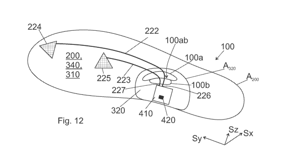
Fig. 12 shows a capacitive sensor for use as an insole, and
Figs. 13a and 13b show capacitive sensors for other uses.
5 Detailed description
As indicated in background, the present invention relates to a capacitive
sensor, e.g. a force and/or a pressure sensor or a touch sensor, with improved
reliability under variable mechanical stress. Preferably, the sensor is
conformable.
In capacitive sensors, the capacitance of an electrode is measured. The
capacitance can be measured relative to surroundings or relative to another
electrode, such a ground electrode. In general there are three working
principles: (1) the dielectric material close to the electrode (e.g. in
between two
electrodes) changes, which changes the capacitance; and/or (2) the distance
between two electrodes changes, which changes the capacitance in between
these electrodes; and/or (3) an area of an electrode changes or a mutual area
between two electrode changes, which changes the capacitance of the
electrode (e.g. relative to another electrode or surroundings). The mutual
area
may change e.g. under shear load. These principles are known to a skilled
person. In a simple form, a capacitance of an electrode relative to its
surroundings changes, when an object is moved close to or away from the
electrode. Typically two electrodes are used for improved accuracy in such a
way that material in between the electrodes is compressed in use. Such
sensors are disclosed in the patent Fl 127245. In touch sensors, the touching
object (e.g. finger of a user) has a different dielectric constant than e.g.
air.
Thus, a capacitance of an electrode changes by movement of the touching
object (according to the working principle 1 above).
Typically in force and/or pressure sensors, an elastic material near the
measuring electrode, e.g. in between two electrodes, is compressed and
deformed at least locally depending on the pressure applied (locally). The
second electrode is not necessarily needed, since typically the object forming
the pressure has a different dielectric constant than the compressed elastic
material, whereby already the deformation causes a change of the capacitance
CA 03112429 2021-03-10
WO 2020/065136 PCT/F12019/050689
6
relative to surroundings. Thus, a local pressure near an electrode can be
determined. Moreover, when multiple electrodes are used at different
locations, multiple local pressures can be determined at different locations.
Force is an integral of the pressure. Therefore, in order to measure a force,
substantially all the measurement area should be covered by the electrodes
used for measurements, as described in the aforementioned patent.
Therefore, in a force sensor, substantially all the measurement area should be
covered by the electrodes used for measurements, while in a pressure sensor
is suffices to provide electrodes used for measurements only to such areas,
where the pressure is to be measured.
As indicated in the background, in order to be widely applicable on bodies
with
various shapes, the sensor, or at least most of the sensor, should be
conformable. Conformable sensors are also usable in such environments,
wherein their shape is subject to change, such as wearable electronics.
Herein the term conformable refers to material that is at least flexible and
stretchable and preferably also compressible. As for the term flexible, a
planar
flexible material can be bent to a radius of curvature of 10 mm (or less)
without
breaking the material at a temperature of 20 C. Moreover, the flexible
material
can be thereafter turned back to the planar form at a temperature of 20 C
without breaking the material; or it may spontaneously turn back to planar
form
without breaking. As for the term stretchable, a stretchable material can be
stretched by at least 10% in a reversible manner. In particular, a layer of
stretchable material can be stretched by at least 10% in a reversible manner
a direction that is perpendicular to the direction of thickness of the layer.
The
reversibility of the stretching is spontaneous, i.e. elastic. As for the term
compressible, a compressible material can be compressed by at least 10 % in
a reversible manner. In particular, a layer of compressible material can be
compressed by at least 10 % in a reversible manner in the direction of
thickness of the layer. The reversibility of the compression is spontaneous,
i.e.
elastic. In this way, a planar conformable material is flexible as indicated
above
and stretchable in a direction of the plane of the planar conformable
material;
and preferably also compressible in the direction of its thickness as detailed
above. A planar conformable material can be arranged to conform a surface
of a hemisphere of a sphere having a radius of 10 cm (or less) at a
temperature
CA 03112429 2021-03-10
WO 2020/065136 PCT/F12019/050689
7
of 20 C without breaking. Typically, a planar conformable material can be
arranged to conform a surface of a hemisphere having a radius of 10 cm (or
less) at a temperature of 20 C without introducing significant plastic (i.e.
irreversible) deformations to the material. Herein the term "significant"
means
.. that, when arranged on the hemisphere, the elastic strain of the
conformable
material is greater than the plastic strain thereof. Thus, a planar
conformable
material can be arranged to conform e.g. a surface of a foot or a fist.
Figs. 2a to 2d show a parts of some sensors. Fig. 2a is a top view, while
Figs.
2b to 2d are side views, as indicated by the directions Sx, Sy, Sz in the
figures.
Sz refers to a direction of thickness of the sensor 100. The directions Sx,
Sy,
and Sz are mutually perpendicular and may depend on location, at least when
the sensor is not planar. As conventional, the term "thickness" refers to a
direction, in which the sensor extends the least. Thus, a thickness is smaller
than a length or a width. Referring to Figs. 2a to 2c, the sensor 100
comprises
electrically conductive wiring 220, which comprises a first electrically
conductive wire 222. The sensor 100 comprises a first electrode 224 for
measuring a capacitance and coupled to the first electrically conductive wire
222. The function of the wire 222 is to couple the electrode 224 to a
measuring
circuit, e.g. via a flexible structure. Therefore, a first joint 226 is joined
to the
first wire 222, as indicated e.g. in Fig. 3a1. The joint 226 is suitable for
joining
the wire 222 to other electronics. The electrode 224 may form a part of the
wiring 220. The wiring 220, in particular the first wire 222 thereof, is
flexible
and stretchable in the meaning discussed above for these terms. Preferably
also the first electrode 224 is flexible and stretchable in the meaning
discussed
above for these terms. As will be detailed below, the wiring 220 may be
arranged as a part of an electrically conductive multilayer structure 200.
Referring to Figs. 3a1 to 3f, the sensor 100 comprises a first electrically
conductive wire 222. The first electrically conductive wire 222 is flexible
and
stretchable in the meaning discussed above for these terms. The first
electrically conductive wire 222 forms at least a part of wiring 220 (see Fig.
2a). The wiring 220 and/or the wire 222 may be manufactured e.g. by using
such additive manufacturing techniques that produce stretchable conductive
wirings, such as printing. In the alternative, the wiring may be laminated
onto
a layer of material. The wiring 220 may be manufactured (e.g. printed or
CA 03112429 2021-03-10
WO 2020/065136 PCT/F12019/050689
8
laminated) onto a flexible and stretchable substrate 210. In the alternative,
the
wiring 220 may be manufactured (e.g. printed or laminated) onto a
compressible layer 310.
Referring to Figs. 3a1 to 3f, the sensor 100 comprises a compressible layer
310. In force and/or pressure sensors, the compressible layer 310 is
configured to be compressed and deform under pressure in use. Moreover,
because of the capacitive operational principle, the compressible layer 310 is
also electrically insulating. Other properties and suitable materials for the
layer
310 are discussed below. When the sensor 100 is used as a touch sensor (i.e.
tactile sensor), a compressible layer 310 is not needed near the electrodes
(224, 225). However, also in touch sensors, the compressible layer 310 may
be used to improve reliability. Therefore, the compressible layer 310 needs
not
to extend so as to overlap with the first electrode 224.
Referring to Figs. 3a1 to 3f, the sensor 100 comprises a reinforcement
structure 320, such as a reinforcement layer. A function of the reinforcement
structure 320 is to connect the first part 100a of the sensor 100 to the
electronic part of the sensor, in particular a flexible board 410. Thus, a
function
of the reinforcement structure 320 is prevent too large in-plane stretching of
the second part 100b of the sensor in between the first part 100a and the
joint
226. In this way, a function of the reinforcement structure 320 is to
reinforce
the sensor 100 at least near a connection of the first wire 222 to other
electronics of the sensor 100. In order to properly reinforce, the
reinforcement
structure 320 is integral, i.e. not constituted from separate parts. Thus the
reinforcement structure 320 extends between each two points of the
reinforcement structure 320. In particular, a first part 320a of the
reinforcement
structure 320 extends to a second part 320b of the reinforcement structure
320 (these parts are to be defined later). These parts (320a, 320b) are
connected directly or via another part of the reinforcement structure 320.
Moreover, preferably, no material interface is arranged in between the first
part 320a and the second part 320b. The first electrically conductive wire 222
and the compressible layer 310 are arranged on a same side of the
reinforcement structure 320. Correspondingly, a part of the reinforcing
structure 320 is not arranged in between the first electrically conductive
wire
222 and the compressible layer 310 in the direction Sz of thickness of the
CA 03112429 2021-03-10
WO 2020/065136 PCT/F12019/050689
9
sensor 100. Preferably, a part of the compressible layer 310 is arranged in
between the first electrically conductive wire 222 and the reinforcement
structure 320 in the direction Sz. However, as indicated in Fig. 3d, a part of
the first electrically conductive wire 222 may be arranged in between the
compressible layer 310 and the reinforcement structure 320. The
reinforcement structure 320 may be or comprise a layer of suitable reinforcing
material. The reinforcement structure 320 may be or form a part of packaging
for a rigid component 420 and/or flexible board 410 of the sensor 100, as in
Fig. 3f. The reinforcement structure 320 may be electrically conductive,
whereby it may be used as a ground electrode, in a similar manner as a
common potential electrode 340. The reinforcement structure 320 may be a
top layer, and can be finished according to needs. Thus, the reinforcement
structure may be used as a top layer 380.
It has been noticed that the stretchability of the first wire 222 can be
utilized to
improve the reliability of the sensor 100. In particular, since the first wire
222
stretchable, its ability to stretch may be utilized to improve reliability.
This
property can be utilized such that, in use, a part of the first wire 222 (i.e.
the
part of the wire 222 within a second part 100b of the sensor as will be
discussed below) takes in most of the mechanical deformations. This can be
achieved by material design in such a way that near a joint 226 the sensor
100, except for the reinforcement structure 320, deforms in-plane more easily
than farther away from the joint 226. The joint 226 is connected to the first
wire
222, and via the first wire 222 to a first electrode 224.
More specifically and with reference to Figs. 3a2, 3b2, and 3e2, the
resilience
of the sensor 100, except for the reinforcement structure, near the joint 226
the sensor 100 can be improved at least by three solutions:
(i) the second part 100b of the sensor 100 comprises a second part
310b of the compressible layer 310, as indicated in Figs. 3a1 and
3a2; and a Young's modulus of the second part 310b of the
compressible layer 310 is less than a Young's modulus of the first
part 310a of the compressible layer 310 or
(ii) the compressible layer 310 does not extend to the second part
100b of the sensor 100, as indicated in Fig. 3b2 or
CA 03112429 2021-03-10
WO 2020/065136 PCT/F12019/050689
(iii) the
thickness T310b of a second part 310b of the compressible layer
310 is less than a thickness T3ioa of a first part 310a of the
compressible layer 310, as indicated in Figs. 3e1 and 3e2.
5 As will
be detailed below, by utilizing at least one of these solutions, the
resilience of a second part 100b of the sensor 100 is improved. In particular,
each one of the alternatives (i) and (iii) has the technical effect that an in-
plane
stiffness of the second part 310b of the compressible layer 310 is less than
an
in-plane stiffness of the first part 310a of the compressible layer 310.
Herein
10 the in-
plane stiffness of the part 310a, 310b refers to the in-plane elastic
modulus of that part as multiplied by the thickness of that part. In this
description, the in-plane elastic modulus is considered equivalent to an in-
plane Young's modulus, a term also commonly used for this property.
As for the alternative (ii), since the compressible layer 310 does not extend
to
the second part 100b, a gap 312 is left next to the first part 310a of the
compressible layer, and, effectively, an in-plane stiffness of a gap is zero.
Thus, all the alternatives (i)-(iii) aim at decreasing the in-plane stiffness
of the
compressible layer within the second part 100b. Moreover, at least a part of
the second part 100b is arranged in between the joint 226 and the first part
100a. Herein the term "in between" refers to being in between in a direction
that is perpendicular to the direction Sz of thickness of the sensor.
However, the other layers of the structure may also affect the resilience. It
has
been found that the reliability is further improved, when the sensor has a
modified first part 100a' with a first in-plane stiffness and a modified
second
part 100b' with a second in-plane stiffness that is lower than the first in-
plane
stiffness, wherein the modified first part 100a' has been modified from the
first
part 100a of the sensor 100 by removing the first part 320a of the
reinforcement
structure 320 and the modified second part 100b' has been modified from the
second part 100b of the sensor 100 by removing the second part 320b of the
reinforcement structure 320. The in-plane stiffness refers to an in-plane
elastic
modulus (Ylooa, Yloob) multiplied by a thickness of the layer. The modified
first
(100a') and second (100b') parts and the corresponding in-plane elastic moduli
are shown in Figs. 3a3, 3b3, and 3c3. Also here, at least a part of the second
part 100b is arranged in between the joint 226 and the first part 100a in a
CA 03112429 2021-03-10
WO 2020/065136 PCT/F12019/050689
11
direction that is perpendicular to the direction Sz of thickness of the
sensor. In
addition, preferably, the whole area in between the joint 226 and the first
part
100a is more resilient than the first part 100a. More precisely, in an
embodiment, the sensor 100 does not have such a part, (i) which is arranged
in between the joint 226 and the first part 100a, and (ii) of which in-plane
stiffness (e.g. elastic modulus) is equal to or greater than the first in-
plane
stiffness (e.g. elastic modulus Yi00,) after removal of the reinforcement
structure 320. More preferably, the sensor 100 does not have such a part, (i)
which is arranged in between the joint 226 and the first part 100a, and (ii)
of
which in-plane stiffness (e.g. elastic modulus), after removal of the
reinforcement structure 320, is higher than the second in-plane stiffness
(e.g.
elastic modulus )(II:lob). In an embodiment, the second part 100b of the
sensor
extends to the joint 226 from a common edge 100ab of the first part 100a and
the second part 100b.
With reference to Figs. 3a1 to 3f, the capacitive sensor 100 has a first part
100a of the capacitive sensor 100 and a second part 100b of the capacitive
sensor 100. Thus, the sensor is dividable to the parts 100a, 100b. Such a
division of the sensor 100 is shown e.g. in Figs. 3a1 to 3d and 4a to 4d by
the
dotted rectangles. The first part 100a extends through the sensor 100 in the
direction Sz of thickness of the sensor 100. The second part 100b extends
through the sensor 100 in the direction Sz of thickness of the sensor. Fig.
3a2
shows the division of the sensor of Fig. 3a1, Fig. 3b2 shows the division of
the
sensor of Fig. 3b1, Fig. 3c2 shows the division of the sensor of Fig. 3c1,
Fig.
4b shows the division of the sensor of Fig. 4a, and Fig. 4d shows the division
of the sensor of Fig. 4c to these two parts. As indicated in Figs. 8a1 to 8b2,
the sensor can be divided to more than two parts. The division is to be
understood as a mental process of defining such parts; the physical sensor
100 is not physically divided. The first part 100a of the sensor 100 and the
second part 100b of the sensor 100 are defined so that they share a common
edge 100ab, as shown in the figures 3a2, 3b2, 3c2, and 12.
The first part 100a of the sensor 100 comprises a first part 320a of the
reinforcement structure 320 (as discussed above), a first part 222a of the
first
electrically conductive wire 222, and a first part of 310a the compressible
layer
310. These layers are arranged relative to each other in such a way that the
CA 03112429 2021-03-10
WO 2020/065136 PCT/F12019/050689
12
first part 320a of the reinforcement structure 320 overlaps, in the direction
Sz
of thickness of the sensor 100, with the first part 222a of the first
electrically
conductive wire 222, or at least a region reasonable close to the first part
222a
of the first electrically conductive wire 222. Thus, the compressible layer
310
transmits the supportive force of the reinforcement structure 320 to the first
electrically conductive wire 222 within the first part 100a. For example, the
reinforcement structure 320 may be provided with an aperture such that the
aperture overlaps the first part 222a of the first electrically conductive
wire 222.
In a preferable embodiment, within the first part 100a, the first part 320a of
the
reinforcement structure 320 radially surrounds such a straight line that is
parallel to the direction Sz of thickness at the location of first part 222a
of the
first wire 222 and penetrates the first part 222a of first wire 222.
Moreover, the first part 320a of the reinforcement structure overlaps, in the
direction Sz of thickness of the sensor 100, with the first part 310a of the
compressible layer 310 (or at least part thereof). Throughout this description
the term overlap refers to parts of layers being arranged, in the direction of
the
thickness Sz of the sensor 100, on top of each other. As indicated e.g. in
Fig.
3b2, the first part 222a of the first electrically conductive wire 222 may be
comprised by a first part 200a of a multilayer conductor structure 200. In
such
a case, preferably, the first part 320a of the reinforcement structure 320
overlaps, in the direction Sz of thickness of the sensor 100, with the first
part
200a of the multilayer conductor structure 200. Moreover, at least a part of
the
first part 310a of the compressible layer 310 overlaps with at least a part of
the
first part 222a the first electrically conductive wire 222 in the direction Sz
of
thickness of the sensor 100. Typically, a part of the first part 310a of the
compressible layer 310 overlaps with the first part 222a the first
electrically
conductive wire 222 in the direction Sz of thickness of the sensor 100.
The second part 100b of the capacitive sensor 100 comprises a second part
320b of the reinforcement structure 320 and a second part 222b of the first
electrically conductive wire 222. These layers may be arranged relative to
each other in such a way that the second part 320b of the reinforcement
structure 320 overlaps with the second part 222b of the first electrically
conductive wire 222 in the direction Sz of the thickness of the sensor 100, or
is at least close to the second part 222b. In a preferable embodiment, within
CA 03112429 2021-03-10
WO 2020/065136 PCT/F12019/050689
13
the second part 100b, the second part 320b of the reinforcement structure 320
radially surrounds such a straight line that is parallel to the direction Sz
of
thickness at the location of second part 222b of the first wire 222 and
penetrates the second part 222b of first wire 222. As indicated e.g. in Fig.
3b2,
the second part 222b of the first electrically conductive wire 222 may be
comprised by a second part 200b of a multilayer conductor structure 200.
As indicated above, in an embodiment, a modified first part 100a' of the
sensor
100, the modified first part 100a' including all other parts of the sensor 100
than the reinforcement structure 320, has a first in-plane elastic modulus
Ylooa
The term in-plane elastic modulus refers e.g. to Young's modulus as
measured in a test, wherein a direction of the deformation is perpendicular to
the direction Sz of thickness of the sensor 100. In such a case, the direction
of the deformation is parallel to a linear combination of the perpendicular
directions Sx and Sy (including Sx and Sy as such). In case the sensor 100 is
planar, the direction of the deformation is in plane of the sensor 100.
Moreover,
in such an embodiment, a modified second part 100b' of the sensor 100, the
modified second part 100b' including all other parts of the sensor 100 than
the
reinforcement structure 320, has a second in-plane elastic modulus Y100b In
.. an embodiment, the second in-plane elastic modulus Y100b is smaller than
the
first in-plane elastic modulus Ylooa. The first and second elastic moduli
Ylooa
and Y100b are indicated in Figs. 3a3, 3b3, and 3c3. Referring in particular to
Figs. 3a3 and 3c3, the second elastic modulus Y100b is smaller, because in
those embodiments, within the second part 100b of the sensor, the material
of the second part 310b of the compressible layer 310 is softer than the
material within the first part 100a of the sensor, i.e. the material of the
first part
310a of the compressible layer. Referring in particular to Fig. 3b3, the
second
elastic modulus may be greater, because the second part 100b does not
comprise a part of the compressible layer 310. However, in such a case, the
in-plane stiffness of the modified second part 100b' is less the in-plane
stiffness of the modified first part 100a', as discussed above. Moreover, in
Fig.
3b2, a gap 312 is formed in between the second part 222b of the wire 222 and
the second part 320b of the reinforcement structure 320. The resilience (or
stiffness) is given in terms of the modified parts 100a' and 100b', since it
has
been noticed that the reinforcement structure 320 can be engineered
CA 03112429 2021-03-10
WO 2020/065136 PCT/F12019/050689
14
according to needs also locally (i.e. separately in both the parts 100a and
100b) without significantly affecting the reliability.
The material of the second part 310b of the compressible layer 310 (if
present)
may have a lower Young's modulus than the material of the first part 310a of
the compressible layer 310, e.g. at least 25 % lower. In case a gap 312 is
used
instead of the material of the second part 310b, the modulus of the gap is
undefined, and practically zero.
With reference to Fig. 3e2, the in-plane stiffness may be affected in addition
or
alternatively by the thickness of the layer(s). As indicated in Fig. 3e2,
within
the first part 100a, the compressible layer 310 may be thicker than within the
second part 100b, whereby a gap 312, of which height is less than the
thickness of the layer 310, is left next to the compressible layer 310.
Therefore,
the in-plane stiffness of the modified first part 100a' of the sensor 100 is
more
than that of the modified second part 100b' of the sensor 100, because the
compressible layer 310 is thinner within the second part 100b. This happens,
even if the materials of the first 310a and second 310b parts of the
compressible layer are the same. The thickness of the first part 310a of the
compressible layer is denoted by T3ioa and the thickness of the second part
310b of the compressible layer is denoted by T310b. In Fig. 3e1, the layer 310
is thinner in the second part 100b because of lack of an adhesive 314, which
is present in the first part 100a and forms a part of the compressible layer
310.
The thickness T310b of the second part 310b may be e.g. at most 98 % of the
thickness T3ioa of the first part 310a in particular if adhesive 314 is used
thicken
the layer 310 only in the first part 100a. In such a case an adhesive 314 is
typically stiffer than the rest of compressible layer.
Figs. 2a to 2d show a parts of sensors, wherein the wiring 220 is arranged as
a part of an electrically conductive multilayer structure 200.
Referring to Fig. 2b, in an embodiment, the sensor 100 comprises a multilayer
conductor structure 200, which comprises the wiring 220 including the first
electrically conductive wire 222. The multilayer conductor structure 200
comprises a flexible and stretchable substrate 210. The substrate is thus
flexible and stretchable in the meaning discussed above for these terms.
CA 03112429 2021-03-10
WO 2020/065136 PCT/F12019/050689
Preferably, the flexible and stretchable substrate 210 is also compressible,
whereby it is preferably conformable. The wiring 220, in particular the first
electrically conductive wire 222, is arranged on the substrate 210. Therefore,
the flexible and stretchable substrate 210 forms an interface 236 with the
first
5 electrically conductive wire 222. With reference to Fig. 3a4, the
substrate 210
can be used to protect the wiring 220 (and the wire 222), at least when the
multilayer conductor structure 200 comprises only the wiring and the substrate
210. Having at least the substrate 210 such that it forms the interface 236
with
the first electrically conductive wire 222 improves the reliability of the
structure,
10 since in such a case, the wire 222 is attached, on at least one side, to
a resilient
layer 210 (see Fig. 2b).
Referring to Fig. 2c, more preferably, the multilayer conductor structure 200
further comprises a flexible and stretchable protective layer 230. The
15 protective layer 230 may further protect at least a part of the wiring
220.
Moreover, in other parts, the protective layer 230 is attached to the
substrate
210. Thus, the wiring 220 is arranged in between the flexible and stretchable
substrate 210 and flexible and stretchable protective layer 230. In an
embodiment, at least a part of the first electrically conductive wire 222 is
arranged in between the flexible and stretchable substrate 210 and the
flexible
and stretchable protective layer 230. Being so arranged, at such locations
that
the wiring does not exists, the protective layer 230 forms a first interface
232
with the flexible and stretchable substrate 210 (see Fig. 2d).
Correspondingly,
at such locations that the wiring 220 exists, the protective layer 230 forms a
second interface 234 with the first electrically conductive wire 222 (Fig.
2c).
Having also the protective layer 230 such that it forms the interface 234 with
the first electrically conductive wire 222 further improves the reliability of
the
structure, since in such a case, the wire 222 is attached, on both sides, to
resilient layers 210, 230 (see Fig. 2c).
In such an embodiment, where the first electrode 224 forms a part of the
wiring
220, at least a part of the first electrode 224 is arranged on the same side
of
the flexible and stretchable substrate 210 as the wiring 220. In such a case,
preferably the (whole) first electrode 224 is arranged on the same side of the
flexible and stretchable substrate 210 as the wiring 220. In case also a
protective layer 230 is used and the first electrode 224 forms a part of the
CA 03112429 2021-03-10
WO 2020/065136 PCT/F12019/050689
16
wiring 220, at least a part of the first electrode 224 is arranged in between
the
flexible and stretchable substrate 210 and the flexible and stretchable
protective layer 230. In such a case, preferably the (whole) first electrode
224
is arranged in between the flexible and stretchable substrate 210 and the
flexible and stretchable protective layer 230.
Preferably the multilayer conductor structure 200 consists of the flexible and
stretchable substrate 210, the flexible and stretchable protective layer 230,
and
the layer or layers in between the flexible and stretchable substrate 210 and
the flexible and stretchable protective layer 230. As indicated above, in an
embodiment, at least a part of the wiring 220 is arranged in between the
flexible
and stretchable substrate 210 and the flexible and stretchable protective
layer
230. However, some adhesive may also be arranged in between the flexible
and stretchable substrate 210 and the flexible and stretchable protective
layer
230 in order to join the layers together.
Preferably, the sensor 100 comprises multiple electrodes, such as the first
electrode 224 and a second electrode 225 (see Fig. 2a). Fig. 2a shows also
other electrodes, even if they do not have their own reference numbers for
clarity. Preferably the electrodes are arranged in such a way that a
capacitance
is measurable using all electrodes simultaneously. In contrast, in some prior
art applications multiplexing is used, whereby only some of the electrodes can
be used at a time to measure the capacitance. In particular, in an embodiment,
the electrodes cover most of the cross-sectional area of the sensor, such as
at
least 50 % or at least 80 % of the cross-sectional area, and the capacitance
is
measurable using all electrodes simultaneously over the whole cross-sectional
area covered by the electrodes.
Thus, in an embodiment, the electrode 224 (or the electrodes 224, 225) define
measurement areas. A measurement area is a part of the sensor 100
extending through the sensor 100 in the direction Sz of thickness. Within a
measurement area, at least one electrode 224 (or 225) is arranged. The
measurement area defined by the electrode is the area, from which
capacitance is configured to be measured by the electrode. Moreover,
electrodes of two different measurement areas are not an a galvanic contact
with each other. Furthermore, a rigid component 420 of the sensor 100 may
CA 03112429 2021-03-10
WO 2020/065136 PCT/F12019/050689
17
be configured to measure a capacitance of each one of the measurement
areas using the electrodes, of which each electrode define one, and only one,
of the measurement areas. Preferably, the rigid component 420 is configured
to measure the capacitance from the whole area of the first electrode 224 at
one instance of time. In other words, preferably, subsequent measurements
are not performed to measure the capacitance from the whole area of the first
electrode 224. This has the beneficial effect that since multiplexing needs
not
be used, the temporal accuracy of the measurement can be improved. More
preferably, for each measurement area, the sensor comprises a wire 222, 223
that is attached in an electrically conductive manner to an electrode 224,
225.
This has the beneficial effect that a capacitance is measurable from each
measurement area simultaneously. Preferably, the first wire 222 is
electrically
connected to only one electrode 224. More preferably, each wire 222, 223, is
electrically connected to only one electrode (224, 225, respectively).
In addition to the extent of the compressible layer 310 or the material
selections of its parts 310a, 310b, it has been noticed that the reliability
can
be further improved by attaching, within the first part 100a of the sensor
100,
the first wire 222, optionally via other layer(s), to the reinforcement
structure
320 in the direction Sz of thickness of the sensor. Attaching in the direction
Sz
of thickness of the sensor does not mean that the reinforcement structure 320
needs to overlap with the first part 222a of the wire 222, e.g. when a layer
of
material is arranged in between the first part 222a of the wire 222 and the
reinforcement structure 320. Referring to Fig. 3a2, the first part 222a of the
wire 222 is attached (in the direction Sz) to the first part 310a of the
compressible layer 310, which is attached (in the direction Sz) to the first
part
320a of the reinforcing structure 320a. This may be done, even if the
reinforcement structure 320 does not overlap with the wire 222, e.g. the
reinforcement structure 320 is provided with an aperture that overlaps with
the
.. wire 222. By attaching the first part 222a of the wire to the reinforcing
structure
320, the reinforcing structure 320 strengthens the structure for improved
reliability.
Furthermore, the reliability can be improved by not attaching, within the
second part 100b of the sensor 100, the second part 222b of the wire 222 to
the second part 320b of the reinforcing structure 320b in the direction Sz of
CA 03112429 2021-03-10
WO 2020/065136 PCT/F12019/050689
18
thickness of the sensor 100; neither directly, nor via other layer(s).
Referring
to Fig. 3a2, in such a case (i) the second part 222b of the wire 222 is not
attached to the second part 310b of the compressible layer and/or (ii) the
second part 310b of the compressible layer is not attached to the second part
320b of the reinforcement structure 320. By not attaching (within the second
part 100b) the wire 222 to the reinforcement structure 320, the wire 222 is
configured to move freely with respect to the reinforcement structure 320,
which allows for the wire 222 to take in the mechanical strain.
In case the first electrically conductive wire 222 forms a part of the
multilayer
conductor structure 200, as discussed above, for manufacturing reasons, it
may be feasible to not attach, within the second part 100b, the second part
200b of the multilayer conductor structure 200 to the second part 320b of the
reinforcement structure 320b, while the first electrically conductive wire 222
remains attached to the other layer 210 or layers 210, 230 of the multilayer
conductor structure 200.
Therefore, in an embodiment, the first part 200a of the multilayer conductor
structure (or the first part 222a of the wire 222, if neither of the layers
210, 230
is used) is attached to a neighboring layer 310, 320, 330; preferably to both
neighboring layers if present; to improve reliability within the first part
100a of
the sensor. Moreover, the neighboring layer is attached to the first part 320a
of the reinforcement structure 320; unless the neighboring layer already is
the
reinforcement structure 320. In an embodiment, the second part 200b of the
multilayer conductor structure is configured to move relatively freely with
respect to the neighboring layer 310, 320, 330 to further improve reliability
near
a connection. As for the term "neighboring layer", this term refers to a layer
that is next to the multilayer conductor structure 200. For example, in Figs.
3a1
to 3a3, the compressible layer 310 forms a neighboring layer for the wire 222.
For example, in Figs. 3b1 to 3c3, the compressible layer 310 forms the
neighboring layer for the multilayer conductor structure 200. In Fig. 3d, both
the reinforcement layer 320 and the compressible layer 310 are neighboring
layers, and either one can be considered as the neighboring layer. In Figs. 4a
to 4d, both the compressible layer 310 and a spacer layer 330 are neighboring
layers, and either one can be considered as the neighboring layer. As for the
term "move relatively freely" and the definition of the second part 100b,
CA 03112429 2021-03-10
WO 2020/065136 PCT/F12019/050689
19
preferably, the whole second part 200b of the multilayer conductor structure
is
configured to move relatively freely with respect to the neighboring layer
310,
320, 330. Thus, in an embodiment, no part of the second part 222b of first
electrically conductive wire 222 is attached, directly or via other layers, in
the
direction Sz of the thickness of the sensor 100, to the second part 320b of
the
reinforcement structure 320.
Within the first part 100a of the sensor, the first part 222a of the first
wire 222
is attached to a neighboring layer or both neighboring layers in the direction
of
thickness Sz of the sensor 100; and further to the first part 320a of the
reinforcement structure 320 (unless the first part 320a already is the
neighboring layer). It may be attached using adhesive. This improves
reliability
within the first part 100a. Moreover, in an embodiment, the second part 222b
of the wire 222 is not attached to second part 320b of the reinforcement
structure 320 (if present). In its part, this allows for the free movement of
the
layers relative to each other.
As indicated above, the relatively free movement is achieved primary by the
extent of the compressible layer 310 or the material selections of its parts
310a,
310b; secondarily by not attaching the second part 222b of the first wire 222
to the second part 320b of the reinforcement structure 320; and tertiarily by
the
different in-plane elastic stiffnesses, defined by the product of the
thickness
and the in-plane modulus Y
= 100a, Y100b of the respective modified part 100a',
100b'.
Outside the reinforcing layer 320, the multilayer conductor structure 200, if
used, is preferably attached to the neighboring layer (310, 330) to help
handling and to improve reliability. If a multilayer conductor structure 200
is
not used, outside the reinforcing layer 320, the first electrically conductive
wire
222 is preferably attached to the neighboring layer (310, 330), which is
adjacent to the wire 222, to help handling and to improve reliability.
To improve the reliability of the connection to other electronics, the first
electrically conductive wire 222 is attached to a first joint 226 for
connecting
the first wire 222 to another electrically conductive structure 400. Such a
joint
226 is shown e.g. in Figs. 3a1, 3a2, 3b2, 3c2, 3d, 4b, 4d, 6b, and 12. Even if
CA 03112429 2021-03-10
WO 2020/065136 PCT/F12019/050689
not shown, such a joint is present in also other embodiments. Such another
electrically conductive structure 400 may be e.g. a flexible circuit board 410
or
a connector 405. A connector 405 may be used to connect the wire 222 e.g.
to a flexible board or a chip. Moreover, in order to use the first joint 226,
the
5 first wire 222, and the first electrode 224 for measurements, the first
electrically
conductive wire 222 extends from the first joint 226 via the second part 100b
of the sensor 100 to the first part 100a of the sensor 100 and further to the
first
electrode 224. The first joint 226 may be arranged within the second part 100b
of the sensor 100; or the first joint 226 may be arranged outside the first
part
10 100a and outside the second part 100b. However, as indicated above, at
least
a part of the second part 100b is arranged in between the joint 226 and the
first part 100a. Herein term "in between" refers to being in between in a
direction (Sx, Sy, or their linear combination) that is perpendicular to the
direction Sz of the thickness of the sensor 100. In a preferable embodiment, a
15 part of the reinforcement structure 320 overlaps with the first joint
226.
However, the reinforcement structure needs not to overlap the first joint 226.
It
suffices that the reinforcement structure 320 radially surrounds at least
partly
such a straight line that is parallel to the direction Sz of thickness at the
location
of the first joint 226 and penetrates the first joint 226. This further
improves the
20 reliability. In another preferable embodiment, a part of the
reinforcement
structure 320 overlaps with at least a part of the flexible circuit board 410.
This
further improves the reliability.
As for the capability of the second part 100b to improve reliability, the
first wire
222 should extend within the second part 100b (e.g. in between the first joint
226 and the first part 100a) for a reasonable length. It has been found that
preferably the first wire 222 extends within the second part 100b such a
distance that is longer than a thickness T310, of the compressible layer 310
within the first part 100a. Thus, and with reference to Figs. 3a2 and 3b2,
preferably, a length L222b of the part 222b of the first wire 222 that extends
within the second part 100b of the sensor 100 is greater than a thickness
T3ioa
of the compressible layer 310 within the first part 100a, i.e. L222b > T310a
(see
Figs. 3a2 and 3b2). In addition or alternatively, the length L222b may be e.g.
at
least 1 mm, at least 2 mm, or at least 5 mm. In case the first wire 222
meanders, the length L222b may be measured along the wire 222.
CA 03112429 2021-03-10
WO 2020/065136 PCT/F12019/050689
21
As indicated above, the multilayer conductor structure 200, if used, is
flexible
and stretchable; and preferably conformable. Moreover, the flexible and
stretchable substrate 210, and, if used, also the flexible and stretchable
protective layer 230 are electrically insulating. E.g. their electrical
resistivities
may be at least 10 cm at a temperature of 23 C. At least the following
materials are suitable for the layers 210 and/or 230: polyurethane,
polyethylene, poly(ethylene-vinyl acetate), polyvinyl chloride, polyborodi-
methylsiloxane, polystyrene, acrylonitrile-butadiene-styrene, styrene-
butad ienestyrene, ethylene propylene rubber, neoprene, cork, latex, natural
rubber, silicone, and thermoplastic elastomeric gel. Either one or both of the
layers 210, 230 may be selected from this group of materials.
As for the wiring 220, in an embodiment, the first wire 222 is made of such
material that is stretchable by at least 10 (:)/0 without breaking. Moreover,
in an
embodiment, the first electrode 224 is made of such material that is
stretchable
by at least 10% without breaking. Such material may be e.g. ink, paste, or
conductive polymer. In an embodiment, the first wire 222 (and optionally the
first electrode 224) comprises some material having an electric conductivity
of
at least 1 S/m at a temperature of 23 C. In an embodiment, the first wire 222
(and optionally the first electrode 224) comprises electrically conductive
particles, such as flakes or nanoparticles, attached to each other in an
electrically conductive manner. In an embodiment, the first wire 222 (and
optionally the first electrode 224) comprises electrically conductive
particles of
some material having an electric conductivity of at least 1 S/m at a
temperature
of 23 C. In an embodiment, the first wire 222 (and optionally the first
electrode
224) comprises electrically conductive particles comprising at least one of
carbon, zinc, nickel, platinum, iron, copper, silver, aluminium, and gold. In
an
embodiment, the first wire 222 (and optionally the first electrode 224)
comprises electrically conductive polymer, such as polyaniline, a polyvinyl
(e.g. polyvinyl alcohol or polyvinyl chloride), and/or PEDOT:PSS (i.e.
poly(3,4-
ethylenedioxythiophene) polystyrene sulfonate). In some electrically
conductive polymers, the conductivity may be the result of electrically
conductive particles as discussed above. What has been said about the
material of the first wire 222 applies, in an embodiment, to the wiring 220
(i.e.
all the wires 222, 223) and/or to all the electrodes (224, 225), optionally
also
to the common potential electrode(s) (340, 350).
CA 03112429 2021-03-10
WO 2020/065136 PCT/F12019/050689
22
The reinforcement structure 320 is a reinforcement in the sense that it has
been observed to improve reliability. It needs not be hard or stiff. With
reference to Fig. 3e1, in an embodiment, the reinforcement may comprise
textile and/or a film. Thus, a top layer similar to a top layer 380 of Fig. 11
may
serve as a reinforcement structure 320. However, as indicated in Fig. 11 the
sensor may comprise both a top layer and a reinforcement structure. As
indicated in Fig. 3e1, the compressible layer 310 may comprise a compressible
body 310' and adhesive 314. The adhesive 314 may attach the compressible
body 310' to the wire 222. The adhesive 314 furthermore thickens the
compressible layer 310 and increases its in-plane stiffness. In Fig. 3e1, the
first part 100a of the sensor 100 comprises the adhesive 314, and the adhesive
314 does not extend to the second part 100b of the sensor. In this way, the
thickness of the compressible layer 310 in the first part 100a is less than in
the
second part 100b. Moreover, the in-plane stiffness of the second part 100b (or
modified second part 100b') is less than the in-plane stiffness of the first
part
100a (or modified first part 100a') due to the absence of the adhesive 314
from
the second part 100b.
However, preferably, the reinforcement structure 320 is a reinforcing in the
sense that it is reasonably thick and reasonably hard. In terms of Young's
modulus, the reinforcement structure 320 may be made of, or at least
comprise, material that has a higher Youngs modulus than each one of: the
compressible layer 310, the flexible and stretchable substrate 210 (if
present),
and the flexible and stretchable protective layer 230 (if present). The
Young's
modulus of the reinforcing structure 320 may be e.g. more than 15 MPa. A
thickness of the reinforcement structure 320 is, in an embodiment, at least
0.1
mm; preferably at least 0.5 mm. The reinforcement structure 320 may
comprise fibrous material, such as at least one of glass fibres, aramid
fibres,
and carbon fibres. The reinforcement structure 320 may comprise polymer,
e.g. polymer having a Young's modulus of more than 15 MPa. Referring to Fig.
3f, the reinforcement structure 320 may be e.g. a package 422 for the other
electronics, such as at least a part of a flexible board 410 and/or a rigid
component 420. When a package 422 of the active electronics of the sensor
100 forms at least a part of the reinforcement structure 320, the
reinforcement
structure 320 may comprise polymer; e.g. polymer having a Young's modulus
of more than 15 MPa; optionally reinforced with fibres as indicated above.
CA 03112429 2021-03-10
WO 2020/065136 PCT/F12019/050689
23
The level of compressibility of the compressible layer 310 may be defined e.g.
in terms of Young's modulus. In an embodiment, the Young's modulus of the
compressible layer 310 is from 0.05 MPa to 15 MPa, such as from 0.2 MPa to
MPa. The electrical resistivity of the compressible layer 310 may be at least
5 10 cm at a temperature of 23 C. Moreover, as the layer 310 is
compressible,
it can be compressed by at least 10 % in a reversible manner.
Same materials are suitable for the compressible layer 310 as for the
substrate
210. Thus, in an embodiment, the material of the compressible layer 310 is
selected from a group consisting of polyurethane, polyethylene, poly(ethylene-
vinyl acetate), polyvinyl chloride, polyborodimethylsiloxane, polystyrene,
acrylonitrile-butadiene-styrene, styrene-butadienestyrene, ethylene propylene
rubber, neoprene, cork, latex, natural rubber, silicone, and thermoplastic
elastomeric gel. Preferably, a thickness T310, of the compressible layer 310
is
at least 0.5 mm.
As for suitable materials for the flexible circuit board 410, these include
polyimide, polyethylene naphthalate, polyethylene terephthalate, and
polyetheretherketone. In an embodiment, the flexible circuit board 410
comprises material selected from a group consisting of these materials. The
flexibility of the flexible circuit board 410 is also a result of the board
410 being
relatively thin. In an embodiment, the a thickness of the flexible circuit
board
410 is less than 1 mm, such as at most 0.5 mm or less than 0.4 mm. In
addition, the flexible circuit board 410 comprises electrically conductive
wiring
as indicated above.
Such materials are flexible, but not reversibly stretchable to a great extent.
Some of the materials may be reversibly stretched for a few percents, but not
as much as defined above for a stretchable material. Because of the low
stretchability, traditional circuit board manufacturing techniques, such as
etching, may be used to produce the flexible board 410 with wiring. Because
of these manufacturing techniques and the wiring material, which is also not
stretchable, the line width can be much smaller than that of the flexible and
stretchable multilayer conductor structure 200. Therefore, in an embodiment,
the flexible board 410 comprises electrically conductive wiring. An electric
conductivity of the wiring of the flexible board 410 may be at least 1 S/m at
a
CA 03112429 2021-03-10
WO 2020/065136 PCT/F12019/050689
24
temperature of 23 C. In an embodiment, the first electrically conductive wire
222 has a first line width, and the wiring of the flexible board 410 comprises
a
wire with a second line width, wherein the second line width is less than the
first line width.
Referring to Figs. 5a and 5b, in an embodiment, the sensor 100 comprises a
rigid component 420. The rigid component 420 is arranged outside of the first
part 100a of the sensor 100. The rigid component 420 is electrically connected
to the first joint 226. Typically the sensor 100 comprises also a second joint
227 and the rigid component 420 is electrically connected to also to the
second
joint 227, and via the second joint 227 to a second wire 223 and further to a
second electrode 225. A rigid component refers to passive electronic
component (e.g. connector) or an active electronic component (e.g. a chip).
The term rigid component refers to a component, of which thickness (i.e.
smallest of three perpendicular measures) is more than 0.1 mm and which
comprises material having a Young's modulus of at least 1 GPa. In addition to
the material with such a high Young's modulus, the rigid component may
comprise another material with a lower Young's modulus. For example, the
rigid component may comprise a chip comprising silicon in addition to some
soft mechanical parts. It is noted that the elastic properties of crystalline
silicon
depend on the orientation, but in general they are in the range of from 60 GPa
to 170 GPa. In an embodiment, a part of the reinforcement structure 320
overlaps with the rigid component 420. This improves the reliability also near
the rigid component 420. In addition, in some application this improves the
comfort of use, since the reinforcement structure 320 spreads the stress
caused by the rigid component 420, e.g. if the sensor 100 is used in an insole
or a mitt.
The rigid component 420 may comprise an electronic chip arrangement
comprising of one or more electronic chips, and optionally packaging related
thereto. The electronic chip arrangement is configured to measure the
capacitance of the first electrode 224. As detailed above, preferably, the
rigid
component 420 is configured to measure the capacitance from the whole area
of the first electrode 224 at one instance of time. More preferably, the rigid
component 420 is configured to measure the capacitance from the whole area
of the first electrode 224 at one instance of time and the capacitance from
the
CA 03112429 2021-03-10
WO 2020/065136 PCT/F12019/050689
whole area of the second electrode 223 at the same or another instance of
time. The capacitance may be measured relative to surroundings or another
electrode, such as a common potential electrode 340. The capacitance may
be transferrable to a receiver in an analog form. However, preferably the
5 electronic chip arrangement is configured to convert the measured
capacitance(s) to a digital signal. Preferably, the rigid component 420
comprises an electronic chip that is configured to convert capacitance(s) to
digital form. Such chips are commonly known as a capacitance to digital
converters (CDC). In an embodiment, the rigid component 420 comprises a
10 capacitance to digital converter.
Referring to Figs. 5a and 5b, in an embodiment, the sensor 100 comprises a
flexible board 410 connected to the first electrically conductive wire 222 via
the
first joint 226. Moreover, in such an embodiment, the flexible board 410 is
15 connected to the rigid component 420. Thus, the rigid component 420 is
connected to the first joint 226 via the flexible board 410. Thus, the rigid
component 420 may be connected to the second joint 227 via the flexible board
410. A wire-to-board connector can be used to connect the rigid component
420 to the flexible board 410. In an embodiment, at least a part of the
flexible
20 board 410 overlaps with a part of the reinforcement structure 320. This
further
improves the reliability near the first joint 226, i.e. between the multilayer
structure 200 and the flexible board 410.
In an embodiment, the flexible board 410 is connected to the first
electrically
25 conductive wire 222 using suitable joining technique, such as crimp
connection or conductive adhesive, such as anisotropic conductive adhesive
(ACF). In such a case, the conductive adhesive may form the first joint 226 or
a part thereof. Conductive adhesives have been found to form reliable joints.
Most preferably, a part of the reinforcement structure 320 overlaps with the
rigid component 420 and another part of the reinforcement structure 320
overlaps with at least a part of the flexible board 410. This improves the
reliability both near the rigid component 420 and near the first joint 226.
The
flexible board 410 may be connected to the second wire 223 in a similar
manner so as to form a part of the second joint 227.
CA 03112429 2021-03-10
WO 2020/065136 PCT/F12019/050689
26
Referring to Figs. 6a and 6b, it has been noticed that the reliability near
the
first joint 226 can be further improved by making the first wire 222 to
meander
near the first joint 226. A meandering wire takes in mechanical stress even
more effectively than a straight wire, even if stretchable. Therefore, in an
embodiment and within the second part 100b of the capacitive sensor 100, the
first electrically conductive wire 222 meanders. The first electrically
conductive
wire 222 may meander at least within the second part 100b such that the first
electrically conductive wire extends from a first point P1 to a second point
P2
in such a manner that a distance between these points (P1, P2), as measured
along the first electrically conductive wire 222, is greater than the distance
between these points (P1, P2) measured straight. Preferably, the first
electrically conductive wire 222 meanders within the second part 100b such
that the first electrically conductive wire extends from a first point P1 to a
second point P2 in such a manner that a distance between these points (P1,
P2), as measured along the first electrically conductive wire 222, is at least
5% greater than the distance between these points (P1, P2) measured
straight. The second point P2 may be located at the first joint 226. The first
point P1 may be located at the common edge 100ab of the first part 100a and
the second part 100b of the sensor 100.
Referring to Fig. 6a, in an embodiment, the first electrically conductive wire
222 meanders (as seen from top) on the substrate 210, e.g. in between the
substrate 210 and the protective layer 230. The substrate 210 needs not to
meander, but it may meander. Thus, the wire 222 may meander (at least) in a
tangential plane of the substrate 210. In addition or alternatively, the
multilayer
conductor structure 200 may meander in the direction Sz of thickness, as
indicated in Fig. 6b. It has been noticed that the meandering particularly in
the
direction Sz of thickness of the sensor improves reliability, since a wire
that
meanders in the Sz direction is extremely resilient in the in-plane direction
(i.e.
perpendicular to Sz). The first electrically conductive wire 222 may meander,
even if only one of or neither one of the substrate 210 and the protective
layer
230 are used.
As motivated above, at least a part, e.g. more than a half, of the sensor 100
is
conformable. However, the reinforcement structure 320 needs not to be
conformable, or at least not as conformable as the rest of the sensor 100.
CA 03112429 2021-03-10
WO 2020/065136 PCT/F12019/050689
27
Referring to Fig. 7, in an embodiment, the first electrically conductive wire
222
extends beyond an edge 322 of the reinforcement structure 320. Thus, a part
of the first electrically conductive wire 222 does not overlap with the
reinforcement structure 320. Moreover, in an embodiment, the reinforcement
structure 320 does not overlap with a part of the first electrode 224.
However,
in an embodiment, the reinforcement structure 320 overlaps with the whole
first electrode 224. Moreover, in an embodiment, the reinforcement structure
320 overlaps with all the electrodes (including 224 and 225). This may improve
reliability.
In terms of cross sectional areas, in an embodiment, a cross-sectional area of
A320 (see Fig. 12) the reinforcement layer is at most 50 % or at most 35 % of
a cross-sectional area A200 (see Fig. 12) of the sensor 100 (e.g. the
multilayer
conductor structure 200). Herein the cross-sectional area refers to an area of
a cross-section that is measured on a tangential surface of the sensor 100. In
case the sensor 100 is substantially planar or can be brought to a
substantially
planar form, the cross-sectional area refers to an area of a cross-section on
a
plane having a normal in the direction Sz of the thickness of the sensor.
Having
this type of relatively small reinforcement layer improves the comfort of use
of
the sensor.
As indicated in many of the figures, a part of the reinforcement structure 320
may overlap with the first electrically conductive wire 222; however as
indicated above, it needs not to overlap. In particular, the first
electrically
.. conductive wire 222 extends from the first joint 226 via the second part
200b
of the multilayer conductor structure to the first part 200a of the multilayer
conductor structure and further to the first electrode 224. In an embodiment,
the first part 200a of the multilayer conductor structure 200 comprises a
first
part 222a of the first wire 222. In an embodiment, the second part 200b of the
multilayer conductor structure 200 comprises a second part 222b of the first
wire 222. In addition to the first wire 222, also the substrate 210 and the
protective layer 230 may extend beyond the edge 322 of the reinforcement
structure 320. Moreover, in this embodiment, also the compressible layer 310
extends beyond the edge 322 of the reinforcement structure 320. As indicated
in Figs. 8a1 to 8b2, in such a case, the sensor 100 is further dividable to a
third part 100c, which extends through the sensor 100 in a direction Sz of
CA 03112429 2021-03-10
WO 2020/065136 PCT/F12019/050689
28
thickness of the sensor 100, and which does not comprise a part of the
reinforcement structure 320. Moreover, the third part 100c of the sensor has
a third in-plane elastic modulus )(II:loc. The third in-plane elastic modulus
Ylooc
may be the same or substantially same as the first in-plane elastic modulus
Yiooc of the modified first part 100a', i.e. the first part 100a without the
reinforcing structure 320. In the alternative, as indicated above and in
particular in connection with touch sensors, the compressible layer 310 and
the common potential electrode 340 need not extend beyond the edge 322. In
such a case, the in-plane stiffness of the third part 100c would be less than
the in-plane stiffness of the modified first part 100a'.
As indicated above, the accuracy of the measurements may be improved by
measuring a capacitance between two electrodes. The other one of the two
electrodes may be referred to as a first common potential electrode 340 (see
Figs. 8a1 and 8b1). In case the potential of the first common potential
electrode
340 is set to a ground potential, the electrode may be referred to as a first
ground electrode. The first common potential electrode 340 may serve as an
electrode that is common to a first pair of electrodes (including the first
common potential electrode 340 and the first electrode 224) and a second pair
of electrodes (including the first common potential electrode 340 and the
second electrode 225). When a part of the compressible layer 310 is left in
between the first common potential electrode 340 and the first electrode 224,
in particular the capacitance of the first electrode 224 relative to the first
common potential electrode 340 can be measured.
Thus, in an embodiment, the sensor 100 comprises a first common potential
electrode 340. Moreover, a part of the compressible layer 310 is arranged in
between the first common potential electrode 340 and the first electrode 224.
In this way, a measurable capacitance is formed in between the first common
potential electrode 340 and the first electrode 224. Preferably, these layers
of
the sensor 100 are arranged relative to each other such that at least a part
of
the first common potential electrode 340 overlaps with at least a part of the
first electrode 224. Moreover, a part of the compressible layer 310 is
arranged
in between the first common potential electrode 340 and the first electrode
224
in the direction Sz of the thickness of the sensor 100. More preferably, at
least
a part of the first common potential electrode 340 overlaps with the whole
first
CA 03112429 2021-03-10
WO 2020/065136 PCT/F12019/050689
29
electrode 224. In an embodiment, first common potential electrode 340 is
connected to the rigid component 420. The first common potential electrode
340 may overlap also the second electrode 225 in a similar manner mutatis
mutandis.
The first common potential electrode 340 may be uniformly conductive, e.g.
made using conductive ink, paste, or conductive polymer on a uniform surface.
As for the conductive material, the materials that are suitable for the first
wire
222 (as discussed above), are suitable also for the conductive material of the
first common potential electrode 340. In the alternative, the first common
potential electrode 340 may be a mesh of conductive yarns, e.g. made using
conductive ink or paste or filaments. It may also suffice that the first
common
potential electrode 340 consists of a meandering electrically conductive line.
It
may also suffice that the first common potential electrode 340 comprises
multiple separate electrically conductive lines. In an embodiment, at least a
part of the first common potential electrode 340 is made from a conductive
ink.
In an embodiment the first common potential electrode 340 comprises
electrically conductive fabric. In an embodiment, the first common potential
electrode 340 comprises electrically conductive polymer (e.g. polyaniline,
polyvinyl, PEDOT:PSS or a polymer with conductive particles).
Referring to Figs. 4a to 4d, the reliability of the sensor 100 may be further
improved by applying a spacer layer 330. The spacer layer 330 may serve as
the neighboring layer discussed above. When the spacer layer 330 is attached
to the first wire 222, optionally via other parts of a multilayer structure
200, also
the spacer layer 330 provides for mechanical support for the wire 222, and in
this way improves reliability, at least when resilience in the second part
100b
is not compromised. As indicated in the figure, at least a part of the first
wire
222 is arranged in between the compressible layer 310 and the spacer layer
330 in the direction Sz of the thickness Sz of the sensor.
The material of the spacer layer 330 may be selected according to needs. In
case the spacer layer 330 needs to be conformable and/or configured to be
compressed in use, the material of the spacer layer 330 may be selected from
the group consisting of polyurethane, polyethylene, poly(ethylene-vinyl
acetate), polyvinyl chloride, polyborodimethylsiloxane, polystyrene,
CA 03112429 2021-03-10
WO 2020/065136 PCT/F12019/050689
acrylonitrile-butadiene-styrene, styrene-butadienestyrene, ethylene propylene
rubber, neoprene, cork, latex, natural rubber, silicone, and thermoplastic
elastomeric gel. However, in case it suffices that the spacer layer 330 is
flexible, also a material selected from the group consisting of polyimide,
5 polyethylene naphthalate, polyethylene terephthalate, and
polyetheretherketone can be used; in addition to some other flexible
materials.
Furthermore, in cases, where the spacer layer 330 needs not be even flexible,
also epoxy and/or phenolic resin may be used as the material of the spacer
layer 330. Preferably the spacer layer 330 is at least flexible, and more
10 preferably also stretchable. In case the spacer layer 330 is not even
flexible,
the whole sensor 100 may be rigid, in which case the structure itself does not
so easily show mechanical reliability problems. In this way, in a preferable
embodiment, at least a part of the sensor 100, such as least a half of the
cross-
section of the sensor 100, is flexible in the meaning defined above. Moreover,
15 in another preferable embodiment, at least a part of the sensor 100,
such as
least a half of the cross-section of the sensor 100 is flexible and
stretchable in
the meanings defined above. A thickness of the spacer layer 330 may be e.g.
at least 0.1 mm, such as at least 0.5 mm. If the spacer layer 330 is used as a
layer that deforms in use, whereby e.g. a capacitance if the first electrode
20 relative to e.g. a second common potential electrode 350 also changes in
use,
a thickness of the spacer layer 330 is preferably at least 0.5 mm. As for
materials suitable for such use, the materials suitable for the compressible
layer 310 are usable also for the spacer layer 330, as indicated above.
25 In case the spacer layer 330 extends to the second part 100b of the
sensor,
as in Figs. 4a, 4b, and 9c, the material of the second part 330b of the spacer
layer 330, which second part 330b is comprised by the second part 100b of
the sensor 100, the second part 330b is preferably made of softer material
than
the first part 330a of the spacer layer 330, which first part 330a is
comprised
30 by the first part 100a of the sensor 100. In the alternative, relative
resilience
can be improved by having the spacer layer 330 in the first part 100a of the
sensor such that the spacer layer 330 does not extend to the second part 100b
of the sensor (see Fig. 8b1).
Referring to Figs. 8b1, 9b, 9d, 10, and 11, in an embodiment, the capacitive
sensor comprises a second common potential electrode 350. Moreover, a part
CA 03112429 2021-03-10
WO 2020/065136 PCT/F12019/050689
31
of the spacer layer 330 is arranged in between the second common potential
electrode 350 and the first electrode 224. In this way, another capacitance of
the first electrode 224, i.e. its capacitance relative to the second common
potential electrode 350, can be measured. Moreover, the other capacitance is
sensitive to pressure, when at least a part of the second common potential
electrode 350 overlaps with at least a part of the first electrode 224. Thus,
in
an embodiment at least the parts of these electrodes 224, 250 overlap in such
a way. The second common potential electrode 350 may overlap the second
electrode 225 in a similar manner mutatis mutandis. What has been said about
the material of the first common potential electrode 340 applies to the
material
of the second common potential electrode 350.
Referring to Figs. 2a, 5a, 5b, and 6a, preferably the multilayer conductor
structure 200 comprises a second electrically conductive wire 223. At least a
part of the second electrically conductive wire 223 may be arranged on the
flexible and stretchable substrate 210, such as in between the flexible and
stretchable substrate 210 and the flexible and stretchable protective layer
230.
The second electrically conductive wire 223 is attached to a second joint 227
for connecting the second wire 223 to the other electrically conductive
structure 400, such as a flexible circuit board 410 or a connector 405.
Moreover, the second electrically conductive wire 223 extends from the
second joint 227 via the second part 100b of the sensor to the first part 100a
of the sensor and further to the second electrode 225. In an embodiment, the
first part 100a of the sensor comprises a first part of the second wire 223.
In
an embodiment, the second part 100b of the sensor comprises a second part
of the second wire 223. Also the second wire 223 is flexible and stretchable
in
the meaning discussed above for these terms. What has been said about the
material of the first wire 222 applies to the material of the second wire 223.
Preferably the second electrode 225 is also flexible and stretchable in the
meaning discussed above for these terms. What has been said about the
material of the first electrode 224 applies to the material of the second
electrode 225.
Referring to Figs. 9a and 9b in an embodiment, the sensor 100 comprises a
bottom layer 360. A part of the compressible layer 100 is arranged in between
the reinforcement structure 320 and the bottom layer 360. In Figs. 9a and 9b,
CA 03112429 2021-03-10
WO 2020/065136 PCT/F12019/050689
32
a part of the first wire 222 is arranged in between the reinforcement
structure
320 and the bottom layer 360. In order to reduce the second in-plane
stiffness,
a gap 312 is arranged between the second part 320b of the reinforcement
structure 320 and the second part 222b of the first wire 222. Thus, the gap
312 is also arranged in between the second part 320b of the reinforcement
structure 320 and the bottom layer 360. In Fig. 9b, also a gap 332 is arranged
between second part 320b of the reinforcement structure 320 and the bottom
layer 360. Such a gap (312, 332) is left, in the direction Sz of thickness, at
the
same level as the neighboring layer (310, 330). Correspondingly, a gap 312
may be left at the level of the compressible layer 310. The level herein
indicate
a distance from the reinforcement structure 320 in the direction Sz of
thickness
of the sensor. In a similar manner, a gap 332 may be left at the level of the
spacer layer 330.
However, referring to Figs. 9c and 9d at least one of the gaps 312, 332 may
be filled with soft material to form a second part or second parts 310b, 330b
of
the compressible layer 310 and/or the spacer layer 330. If the material of the
second part 310b of the compressible layer 310 is softer than the material of
the first part 310a of the compressible layer 310, the in-plane elastic
modulus
-- Y100b of the modified second part 100b' of the sensor is smaller than the
in-
plane elastic modulus Yloo, of the modified first part 100a' of the sensor. In
this
way, the second part 200b of the multilayer conductor structure is configured
to take in mechanical deformation in use. Herein the first part 100a of the
sensor 100 comprises the first part 310a of the compressible layer 310 and the
-- second part 100b of the sensor 100 comprises the second part 310b of the
compressible layer 310. In this case the material of the neighboring layer 310
is softer within the second part 100b of the capacitive sensor 100 than the
material of the neighboring layer 310 within the first part 100a of the
capacitive
sensor 100.
The same finding applies also to the spacer layer 330. If the material of the
second part 330b of the spacer layer 330 is significantly softer than the
material
of the first part 330a of the spacer layer 330, the second part 200b of the
multilayer conductor structure is configured to take in the mechanical
-- deformations. Herein the first part 100a of the sensor 100 comprises the
first
part 330a of the spacer layer 330 and the second part 100b of the sensor 100
CA 03112429 2021-03-10
WO 2020/065136 PCT/F12019/050689
33
comprises the second part 330b of the spacer layer 330. In this case the
material of the neighboring layer 330 is softer within the second part 100b of
the capacitive sensor 100 than the material of the neighboring layer 330
within
the first part 100a of the capacitive sensor 100. The material of the second
part 330b of the spacer layer layer 330 (if present) may have a lower Young's
modulus than the material of the first part 330a of the spacer layer 330, e.g.
at
least 25 % lower.
The sensor 100 may comprise further layers. Referring to Fig. 10, the sensor
100 may comprise a second reinforcement structure 370, such as a second
reinforcement layer 370; in which case the reinforcement structure 320 may
be referred to as a first reinforcement structure 320. A part of the first
wire 222
and a part of the compressible layer 310 are arranged in between the (first)
reinforcement structure 320 and the second reinforcement structure 370. At
least a part of the common potential electrode 340, if present, may be
arranged
in between the first reinforcement structure 320 and the second reinforcement
structure 370. At least a part of the second common potential electrode 350,
if
present, may be arranged in between the first reinforcement structure 320 and
the second reinforcement layer structure. At least a part of the spacer layer
330, if present, may be arranged in between the first reinforcement structure
320 and the second reinforcement structure 370. Herein the term "in between"
refers to the direction Sz of thickness. However, if the sensor 100 comprises
both the second reinforcement structure 370 and the bottom layer 360,
preferably, both the first reinforcement structure 320 and the second
reinforcement structure 370 are arranged on a same side of the bottom layer
360. Thus, the bottom layer 360 may be finished e.g. for visual appearance of
the sensor and/or for improved comfort of use. The second reinforcement
structure 370 may be made of such a material that has been discussed above
to be suitable for the first reinforcement structure 320.
Referring to Fig. 11, the sensor 100 may comprise a top layer 380. The
reinforcement structure 320, a part of the first wire 222, and a part of the
compressible layer 310 are arranged on a same side of the top layer 380.
Thus, the top layer 380 may be finished e.g. for visual appearance of the
sensor and/or for improved comfort of use. Preferably, the top layer 380 is
made of textile (synthetic or natural). In an embodiment, the top layer 380
CA 03112429 2021-03-10
WO 2020/065136 PCT/F12019/050689
34
comprises fibrous material. In an embodiment, the top layer 380 comprises
woven fibrous material. The sensor may comprise the top layer 380 even if
does not comprise one or more than one of the following layers: the second
reinforcement layer 370, the bottom layer 360, the (first) common potential
electrode 340, the second common potential electrode 350, and the spacer
layer 330.
Thus, as discussed in detail above, the reliability may be improved by
allowing
the second part 222b of the first electrically conductive wire 222 to move
relatively freely in relation to the reinforcement structure. The following
two
alternatives were identified:
- using a layer (310, 330), of which at least a part does not extend in a
lateral direction (i.e. perpendicular to the direction Sz of thickness) as
far as the wire 222. As a result a gap 312, 332 is formed, which in
effect reduces the in-plane stiffness of the second part 100b; and
- using a softer material for the layer (310, 330) within the second part
100b than within the first part 100a.
As for the first option, it suffices that a thin part (e.g. the body 310') of
the layer
(310, 330) extends in the lateral direction when another part (e.g. adhesive
314) does not extend, thereby forming a gap.
Even if not shown in the figures, it is possible to use a layer (310, 330)
having
both a soft area (310b, 330b, e.g. within the second part 100b) and a hard
area
(within the first part 100a), and to further have such a gap (312, 332) that
the
gap is left between the joint 226 and the soft are (310b, 330b).
Moreover, as discussed in detail above, the reliability may be further
improved,
on one hand, by attaching in the direction Sz of the thickness, within the
first
part 100a, the first electrically conductive wire 222 to the reinforcement
structure 320 and by not attaching the first electrically conductive wire 222
to
the reinforcement structure 320 within the second part 100b in the direction
Sz
of the thickness. Not attaching may be achieved by using a gap (312, 332) or,
in case the gap is filled, not attaching the material that fills the gap to at
least
a layer next to the material that fills the gap.
CA 03112429 2021-03-10
WO 2020/065136 PCT/F12019/050689
Furthermore, the in-plane stiffness of the modified parts (100a', 100b') may
be
engineer as discussed above to further improve reliability. Possibilities
include
engineering the elastic moduli (Y
, . 100a, Y100b) of the modified parts (100a', 100b')
and/or engineering the thicknesses of the modified parts (100a', 100b').
5
Such a sensor can be used in various application including, but not limited
to,
clothing, such as gloves, mitts, footwear (shoes, insoles, socks), helmets,
etc.
In clothing, particularly two applications may be pointed out: a boxing glove
and an insole for footwear. Other applications include scales for measuring
10 mass and tactile sensors e.g. for various user interface devices.
To this end, Fig. 12 shows a sensor 100, the sensor 100 being shaped as an
insole for footwear. The measuring electronics, including a rigid component
420, such as a chip, is arranged at a location, which in use, is arranged
15 beneath the arch of a foot. The component 420 is attached to a flexible
board
410, which is attached to a first wire 222 of a multilayer conductor
structure,
which is flexible and stretchable. The component 420, the flexible board 410,
and a part of the first wire 222 are arranged beneath a reinforcement
structure
320. The sensor 100 extends laterally outside the reinforcing layer 320, and
20 comprises ¨ also outside the reinforcement structure 320 ¨ a part of the
multilayer conductor structure 200 and a part of the compressible layer 310;
and typically also a part of the common potential electrode 340. The first
electrode 224 forms a part of the wiring of the multilayer conductor structure
200, and is arranged in between the flexible and stretchable substrate 210 and
25 the flexible and stretchable protective layer 230. A possible selection
of the
first part 100a and the second part 100b of the sensor 100 are indicated in
Fig.
12. As indicated above, both the first and second parts (100a, 100b) are
selected such that both of them comprise a part of the reinforcement structure
320. As discussed above, an in-plane elastic modulus Ylooa of the modified
30 first part 100a' may be greater than an in-plane elastic modulus Y100b
of the
modified second part 100b'. Moreover, in the embodiment of Fig. 12, within
the first part 100a, the multilayer conductor structure 200 is attached to the
compressible layer 310, e.g. using an adhesive. In addition, outside the
reinforcement structure 320, the multilayer conductor structure 200 is
attached
35 to the compressible layer 310. When the sensor is used as an insole, the
multilayer conductor structure 200 takes in stress by deformations due to the
CA 03112429 2021-03-10
WO 2020/065136 PCT/F12019/050689
36
different in-plane elastic moduli. Even if Fig. 12 shows a sensor 100 with
only
two electrodes, the sensor can be provided with multiple electrodes according
to needs. For example, the sensor 100 may be provided with an electrode
configuration disclosed in the patent Fl 127245.
Figures 13a and 13b show some other shapes for the sensor for other
applications than an insole.