Note: Descriptions are shown in the official language in which they were submitted.
1
HIGH EFFICIENCY COMPACT SLOTTED ANTENNA WITH A GROUND PLANE
TECHNICAL FIELD OF THE INVENTION
[0001] The present invention relates to methods of making a high efficiency
compact slotted
antenna with a ground plane from one or two photodefinable glass substrate
wafers.
BACKGROUND OF THE INVENTION
[0002] Without limiting the scope of the invention, its background is
described in connection
with high efficiency compact slotted antenna.
[0003] A slot antenna consists of a metal surface, usually a flat plate, with
one or more holes
or slots cut out of a metal substrate/ground plane. In general, these slots
are about are about
k/4 long with a centers to center spacing of 212 separation. The emitter or
source is generally
placed 214 from the first slot and the center of the last slot is 214 from the
end or reflector of
the waveguide. The reflector or end of waveguide requires a precision of ¨
2110. A one-
centimeter wavelength requires a reflector placement precision of one
millimeter. The
widths of the slots are much less than the wavelength of the emission. The
shape and size of
the slot, as well as the driving frequency, determine the radiation pattern.
Slot antennas are
widely used in radar antennas in marine radar, cell phone base stations, and
desktop
microwave sources for research and calibration purposes. A slot antenna's main
advantages
are its design simplicity and convenient adaptation to mass production for
frequencies
between 1 GHz and 25 GHz. The width of the waveguide is approximately the free
space
wavelength (2.) of the emission and the height of the waveguide is 2110. You
can see that at
1 GHz or wavelength of 29.9 cm up to a frequency of 25 GHz or wavelength of
1.19 cm
classic computer numerical control (CNC) tools have sufficient precision to
create slotted.
However, at 100 GHz or wavelength of 0.299 cm requires a transverse slot
dimension <<
on the order of 0.003 cm (1.1 mil). A modern CNC tool has a precision of 0.01
cm +/- 0.01
cm or ¨3.9 mil +/- 0.4 mil. Clearly at higher frequencies or shorter
wavelengths the ability
to use classical CNC machining becomes unrealizable.
Date Recue/Date Received 2021-08-19
2
SUMMARY OF THE INVENTION
[0004] Slotted antenna are considered simple to fabricate using classic
machining techniques
at frequencies between 600 MHz and 25 GHz. Above 30 GHz the precision and
feature size
for making the slots, waveguides, and frequency launching elements. As an
example, the
center-to-center spacing at a frequency of 100 GHz is 2/2 or 1.5 mm, the
termination of the
waveguide is 2/4 or 750 m from the center of the last slot with a precision of
2/10 or 150
p.m, the width of the slots are <<2k. or 15011m, the width of the waveguide is
approximately
the free space wavelength (k or 3mm) of the emission and the height of the
waveguide is
2/10 or 150 [rm. The level of precision required for slot antenna exceeds
classic CNC
machining capability to produce low cost high quality slotted antenna. However
printed
circuit board (PCB) and/or semiconductor processing technology the ability to
produce
feature sizes much less than a micrometer. The materials used in PCB and
semiconductor
technology are electronically lossy i.e; they have a high loss tangent and not
support the
creation or production of an efficient low cost slot antenna. DuPont has shown
the use of a
LTCC (low temperature co-fired ceramic) multilayer slotted antenna. The LTCC
antenna
was prototyped by etching pattern green (unfired/sintered) ceramic and then
filling the
pattern with a refractory metal. The cavity of the antenna consisted of the
ceramic material.
The individual layers of the green LTCC were then hand assembled much like a
deck of
cards and then sintered/fired to form a slotted antenna. The green ceramic
shrinks about
8.5% in the plane direction of the ceramic when fired/sintered. The shrinkage
causes stress
and misalignment of the individual elements of the slotted antenna. This LTCC
slotted
antenna had reasonable performance but was determined not to be cost
effective. The RF
properties for LTCC include a loss tangent of 0.0012 and a dielectric constant
of 7.1 +/-0.2.
Several of the devices were prototyped and tested. These values for the loss
tangent and
dielectric constant are good compared to other efforts to make a miniature
slotted antenna
but they fall into the poor category when compared to large slotted antennas
that have air as
the dielectric media. Air has a loss tangent of 0.00 and a dielectric constant
of 1.00059.
Unfortunately, the yield and performance of the ceramic prevented the LTCC
slotted antenna
technology form being viable. Classic MEMS based processing is not able to
produce a
viable technical approach due to the inherent stress from the thick deposition
in the materials
that are added or subtracted. Thin films have stress building up from the
deposition process
that is sufficient to cause a delamination in thicker device structures. The
present invention
is a photodefinable glass based slotted antenna that uses air as its
dielectric media using
Date Recue/Date Received 2021-03-11
3
semiconductor/printed circuit board (PCB) processing in a photodefinable glass
and low
stress electroplating metallization technology.
[0005] In one embodiment, the present invention includes a method of making a
slotted
waveguide antenna structure with matched ground plane comprising: forming in a
photosensitive glass substrate a coaxial-to-coplanar waveguide (CPW) section
connected to
a power divider that is connected to an emission cavity area for the slotted
antenna and one
or more vias; depositing a metal ground plane to a first surface of the
photosensitive glass
substrate; depositing a copper layer on the photosensitive glass substrate
with a pattern of
slots that form a slot antenna above the emission cavity; forming one or more
copper pillars
in the emission cavity under the slot antenna; etching away the photosensitive
glass in the
emission cavity while retaining the one or more copper pillars; connecting a
micro coaxial
connector to the coaxial-to-coplanar waveguide (CPW) section; and one or more
solder
bumps at the vias that connect to the ground plane, to form a slotted antenna.
In one aspect,
the photodefinable glass substrate is a glass substrate comprising a
composition of: 60 - 76
weight % silica; at least 3 weight % 1(20 with 6 weight %- 16 weight % of a
combination of
K20 and Na2O; 0.003-1 weight % of at least one oxide selected from the group
consisting of
Ag2O and Au20; 0.003-2 weight % Cu2O; 0.75 weight % - 7 weight %B203, and 6 -
7 weight
% A1203; with the combination of B203; and Al2O3 not exceeding 13 weight %; 8-
15 weight
% Li20; and 0.001 ¨ 0.1 weight % Ce0?. In another aspect, the photodefinable
glass
substrate is a glass substrate comprising a composition of: 35 - 76 weight %
silica, 3- 16
weight % 1(20, 0.003-1 weight % Ag2O, 8-15 weight % Li2O, and 0.001 ¨ 0.1
weight %
Ce02. In another aspect, the photodefinable glass substrate is at least one
of: a photo-
definable glass substrate comprises at least 0.1 weight % Sb203 or As203; a
photo- definable
glass substrate comprises 0.003-1 weight % Au20; a photo-definable glass
substrate
comprises 1-18 weight % of an oxide selected from the group consisting of CaO,
ZnO, Pb0,
MgO, Sr0 and BaO; and optionally has an anisotropic-etch ratio of exposed
portion to said
unexposed portion is at least one of 10-20:1; 21-29:1; 30-45:1; 20-40:1; 41-
45:1; and 30-50:1.
In another aspect, the photodefinable glass substrate is a photosensitive
glass ceramic
composite substrate comprising at least one of silica, lithium oxide, aluminum
oxide, or
cerium oxide. In another aspect, the method further comprises dicing one or
more of the
slotted antennas from the photodefinable glass substrate into individual
slotted antennas. In
another aspect, the slotted antenna comprises one or more slot openings above
a cavity,
wherein the slotted portion of the antenna is supported with one or more glass
or copper
pillars in the cavity.
Date Recue/Date Received 2021-03-11
4
[0006] In another embodiment, the present invention includes a two-wafer
method of
making a slotted antenna comprising: forming on a first surface of a first
photodefinable
glass substrate wafer: one or more copper support pillars in a cavity, one or
more outside
walls for the cavity, and a copper via for connecting a micro axial connector,
and on a
second surface of a first photodefinable glass substrate wafer a copper layer
that comprises
one or more antenna slots; forming on a first surface of a second
photodefinable glass
substrate wafer: a micro axial connector and power divider section, a
resonator cavity, side
walls, and one or more support structures in the resonator cavity; and placing
solder balls
along a metal surface of an emission cavity slotted antenna section, the
support structures in
the cavity, a power divider section, and a coaxial-to-coplanar waveguide (CPW)
of at least
one of the first or second photodefinable glass substrate wafers; aligning the
first and second
photodefinable glass substrate wafers at the slotted antenna; and compressing
the first or
second photodefinable glass substrate wafers at a temperature sufficient to
flow the solder
balls to connect the support structures in the cavity, a power divider
section, and a coaxial-
to-coplanar waveguide of the first and second photodefinable glass substrate
wafers; and
forming a slotted antenna on a surface of the second photodefinable glass
substrate wafer
opposite the cavity in the first photodefinable glass substrate wafer. In one
aspect, the
photodefinable glass substrate is a glass substrate comprising a composition
of: 60 - 76
weight % silica; at least 3 weight % K20 with 6 weight %- 16 weight % of a
combination of
1(20 and Na2O; 0.003-1 weight % of at least one oxide selected from the group
consisting of
Ag2O and Au20; 0.003-2 weight % Cu2O; 0.75 weight % - 7 weight %B203, and 6 -
7
weight % A1203; with the combination of B203; and A1203 not exceeding 13
weight %; 8-15
weight % Li2O; and 0.001 ¨ 0.1 weight % Ce02. In another aspect, the
photodefinable glass
substrate is a glass substrate comprising a composition of: 35 - 76 weight %
silica, 3- 16
weight % 1(20, 0.003-1 weight % Ag2O, 8-15 weight % Li2O, and 0.001 ¨ 0.1
weight %
Ce02. In another aspect, the photodefinable glass substrate is at least one
of: a photo-
definable glass substrate comprises at least 0.1 weight % Sb203 or As203; a
photo- definable
glass substrate comprises 0.003-1 weight % Au20; a photo-definable glass
substrate
comprises 1-18 weight % of an oxide selected from the group consisting of CaO,
ZnO, Pb0,
MgO, Sr0 and BaO; and optionally has an anisotropic-etch ratio of exposed
portion to said
unexposed portion is at least one of 10-20:1; 21-29:1; 30-45:1; 20-40:1; 41-
45:1; and 30-
50:1. In another aspect, the photodefinable glass substrate is a
photosensitive glass ceramic
composite substrate comprising at least one of silica, lithium oxide, aluminum
oxide, or
cerium oxide. In another aspect, the method further comprises dicing one or
more of the
Date Recue/Date Received 2021-03-11
5
slotted antennas from the photodefinable glass substrate into individual
slotted antennas. In
another aspect, the slotted antenna comprises one or more slot openings above
a cavity,
wherein the slotted portion of the antenna is supported with one or more glass
or copper
pillars in the cavity.
[0007] In yet another embodiment, the present invention includes a method of
making a
slotted waveguide antenna structure with matched ground plane comprising: (1)
masking a
design layout comprising one or more structures to form one or more electrical
conduction
paths on a photodefinable glass substrate; (2) exposing at least one portion
of the
photosensitive glass substrate to an activating energy source to expose one or
more
sidewalls and one or more support elements of an antenna structure; (3)
processing the
photosensitive glass substrate to a heating phase above its glass transition
temperature to
convert a portion of the photodefinable glass substrate exposed the activating
energy source
into a ceramic, wherein the portion of the photodefinable glass formed into a
ceramic
comprises an outside, inside walls, and at least one via of the antenna
structure; (4)
depositing a layer of tantalum and a layer of copper on a first side of the
photodefinable glass
substrate; (5) coating the photodefinable glass substrate with a photoresist
to form an interior
of a coaxial-to-coplanar waveguide (CPW) connected to a power divider that is
connected to
an emission cavity for the slotted antenna; (6) etching one or more sidew-alls
and one or
more support vias in the substrate; (7) depositing a photoresist the protects
the coaxial-to-
coplanar waveguide (CPW) and the power divider; (8) exposing the
photosensitive glass
substrate to an activating energy source to expose the emission cavity for a
time sufficient to
form the cavity without crossing the wafer; (9) removing the photoresist and
processing the
photosensitive glass substrate to a heating phase above its glass transition
temperature to
convert the photodefinable glass substrate exposed to the activating energy
source into a
ceramic; (10) coating and exposing a photoresist on a second side of the
photodefinable glass
substrate with a pattern of slots that form a slot antenna; (11) depositing a
layer of tantalum
and a layer of copper on the second side of the photodefinable glass
substrate; (12) removing
the photoresist and electroplating with copper the photodefinable glass
substrate; (13)
coating the photodefinable glass substrate with a photoresist except for the
portion of the
emission cavity, and exposing the power divider and coaxial to CPW sections;
(14) etching a
portion of the photodefinable glass substrate formed into a ceramic for a time
sufficient to
form the emission cavity, without traversing the photodefinable glass
substrate; (15) rinsing
the wafer with water or a solvent; (16) using a projection aligner exposing a
region with a
pattern to form one or more glass pillars or glass pillar regions in the
emission cavity; (17)
Date Recue/Date Received 2021-03-11
6
coating the photodefinable glass substrate to silver nitrate and reducing the
silver nitrate to
metallic silver on the photodefinable glass substrate with an infrared source
on the power
divider and coaxial to CPW sections; (18) electroless plating copper on the
metallic silver;
(19) heating the photodefinable glass substrate to at least 250 C in argon to
adhere the
copper to the silver; (20) etching with a spin on glass SiO2 with a plasma
etching process to
expose the copper sidewalls around the power divider and coaxial to CPW
sections; (21)
plasma etching down to one or more copper sidewalls; (22) coating the
photodefinable glass
substrate with photoresist and open the region over the spin on glass over
where a contact tab
for the power divider and coaxial to CPW sections and plasma etching down to a
copper tab;
(23) removing the photoresist using a standard stripper the rinse with water;
(24) coating the
photodefinable glass substrate with a photoresist clearing a pattern over the
power divider;
(25) sputtering coating the photodefinable glass substrate with tantalum and
then copper;
(26) electroless plating copper on the sputtered copper; (27) removing the
photoresist and
rinsing the photodefinable glass substrate with water; (28) depositing a
solder bump with an
ink jet printer to form an electrical contact with a center electrode of a
micro coaxial
connector of the coaxial to CPW element; (29) heating the photodefinable glass
substrate to
allow the solder bump to flow making a solid electrical and mechanical
connection from the
electrical contact of the coaxial to CPW element; (30) rinsing the wafer in
10% HF, to
remove all of the remain ceramic material and spin on glass from the antenna
cavity; (31)
rinsing the wafer with water and alcohol; and (32) depositing a solder bump
bond with an
ink jet deposition process at a perimeter of the slotted antenna to make
contact with a ground
plane and to attach the micro coaxial connector to the photodefinable glass
substrate; and at
the center electrode of the micro coaxial connector to the coax to CPW
element; (33)
attaching a surface mount micro coaxial connector to the solder bumps, to
provide a coaxial
connector to the slotted antenna. In one aspect, the activating energy source
is a UV light. In
another aspect, the photodefinable glass substrate is a glass substrate
comprising a
composition of: 60 - 76 weight % silica; at least 3 weight % K20 with 6 weight
%- 16 weight
% of a combination of 1(20 and Na2O; 0.003-1 weight % of at least one oxide
selected from
the group consisting of Ag2O and Au20; 0.003-2 weight % Cu2O; 0.75 weight % -
7 weight
%B203, and 6 - 7 weight % A1203; with the combination of B203; and A1203 not
exceeding 13
weight %; 8-15 weight % Li2O; and 0.001 ¨ 0.1 weight % Ce02. In another
aspect, the
photodefinable glass substrate is a glass substrate comprising a composition
of: 35 - 76
weight % silica, 3- 16 weight % K20, 0.003-1 weight % Ag2O, 8-15 weight %
Li2O, and
0.001 ¨ 0.1 weight % Ce02. In another aspect, the photodefinable glass
substrate is at least
Date Recue/Date Received 2021-03-11
7
one of: a photo-definable glass substrate comprises at least 0.1 weight %
Sb203 or As203; a
photo- definable glass substrate comprises 0.003-1 weight % Au20; a photo-
definable glass
substrate comprises 1-18 weight % of an oxide selected from the group
consisting of CaO,
ZnO, Pb0, MgO, Sr0 and BaO; and optionally has an anisotropic-etch ratio of
exposed
portion to said unexposed portion is at least one of 10-20:1; 21-29:1; 30-
45:1; 20-40:1; 41-
45:1; and 30-50:1. In another aspect, the photodefinable glass substrate wafer
is a
photosensitive glass ceramic composite substrate comprising at least one of
silica, lithium
oxide, aluminum oxide, or cerium oxide. In another aspect, the method further
comprises
dicing one or more of the slotted antennas from the first and second
photodefinable glass
substrate wafers into individual slotted antennas. In another aspect, the
slotted antenna
comprises one or more slot openings above a cavity, wherein the slotted
portion of the
antenna is supported with one or more glass or copper pillars in the cavity
formed between
the first and second photodefinable glass substrate wafers
[0008] In yet another embodiment, the present invention includes a two-wafer
method of
making a slotted antenna comprising: (1) processing a first photodefinable
glass substrate
wafer by: depositing a photoresist or wax on a first surface of a first
photodefinable glass
substrate wafer; exposing a pattern on the first photodefinable glass
substrate wafer to
expose one or more sides of an emission cavity, one or more vias, and one or
more support
structures of an antenna structure; thermally cycling the first photodefinable
glass substrate
wafer to convert the exposed material to a ceramic; coating, exposing and
developing a
photoresist on the first side of the first photodefinable glass substrate
wafer into slots for RF
emissions; depositing tantalum and copper on the photoresist by sputtering on
the first
surface of the first photodefinable glass substrate wafer; electroplating
copper on the first
photodefinable glass substrate wafer; coating the first surface of the first
photodefinable
glass substrate wafer with a wax, a photoresist or other protective coating;
etching the one or
more vias and the one or more support structures; electroplating the one or
more vias and the
one or more support structures and the one or more sidewalls of the antenna;
performing
chemical-mechanical polishing of a second surface of the first photodefinable
glass substrate
wafer opposite the first surface of the first photodefinable glass substrate
wafer; exposing the
emission cavity to an activating energy to expose the emission cavity, a power
divider and a
coaxial-to-coplanar waveguide (CPW) section; thermally cycling the first
photodefinable
glass substrate wafer to convert the exposed material to a ceramic phase; (2)
processing a
second photodefinable glass substrate wafer by: forming on a first surface of
the second
photodefinable glass substrate wafer a micro coaxial connector and power
divider section
Date Recue/Date Received 2021-03-11
8
with a photo mask; exposing one or more sidewalls of an emission cavity, and
one or more
support structures; thermally cycle the second photodefinable glass substrate
wafer to
convert the exposed material to a ceramic phase; coating, exposing and
developing a
photoresist on a second surface of the second photodefinable glass substrate
wafer substrate
with a pattern for an external copper slotted antenna; depositing tantalum and
copper on the
photoresist by sputtering on the first surface of the second photodefinable
glass substrate
wafer; removing the photoresist using a standard stripper and electroplating
copper on the
second photodefinable glass substrate wafer; coating a second surface of the
second
photodefinable glass substrate wafer with a wax, a photoresist or other
protective coating;
etching the one or more sidewalls and one or more support pillars;
electroplating the one or
more pillars and one or more sidewalls from the copper on the first surface of
the second
photodefinable glass substrate wafer; rinsing with water and drying the second
photodefinable glass substrate wafer; flattening a second surface of the
second
photodefinable glass substrate wafer my chemical¨mechanical polishing;
coating, exposing
and developing a photoresist on the first surface of the second photodefinable
glass substrate
wafer to shield the micro coaxial connector power divider section; exposing
the second
photodefinable glass substrate wafer to an activating energy; thermally
cycling the second
photodefinable glass substrate wafer to convert the exposed material to a
ceramic phase;
depositing tantalum and copper on the photoresist by sputtering on the first
surface of the
second photodefinable glass substrate wafer; removing the photoresist using a
standard
stripper and electroplating copper on the second photodefinable glass
substrate wafer to
expose the openings; and (3) connecting the first and second photodefinable
glass substrate
wafers, by: placing solder balls on the copper elements of the front surface
of the first
photodefinable glass substrate wafer: using alignment fiducials and etched
keyed structure to
align the first and second photodefinable glass substrate wafers; compressing
the first and
second photodefinable glass substrate wafers to keep the alignment; heating
the aligned first
and second photodefinable glass substrate wafers to flow the solder into a
solid electrical and
mechanical connection at the coax to CPW element; coating the joined first and
second
photodefinable glass substrate wafers with photoresist to expose the slot
patterns; coating a
second side of the first and second photodefinable glass substrate wafers with
wax,
photoresist or other material to protect the first and second photodefinable
glass substrate
wafers; etching the joined first and second photodefinable glass substrate
wafers to remove
the ceramic phase from the resonator, power divider and coax to CPW sections;
removing
the photoresist; exposing the one or more slot patterns on the joined first
and second
Date Recue/Date Received 2021-03-11
9
photodefinable glass substrate wafers; and etching the joined first and second
photodefinable
glass substrate wafers to open the one or more slot patterns. In one aspect,
at least one of the
first and second photodefinable glass wafers is a glass substrate comprising a
composition
of: 60 - 76 weight % silica; at least 3 weight % K20 with 6 weight %- 16
weight % of a
combination of 1(20 and Na2O; 0.003-1 weight % of at least one oxide selected
from the
group consisting of Ag2O and Au20; 0.003-2 weight % Cu2O; 0.75 weight % - 7
weight
%B203, and 6 - 7 weight % A1203; with the combination of B203; and Al2O3 not
exceeding
13 weight %; 8-15 weight % Li2O; and 0.001 ¨ 0.1 weight % Ce02. In another
aspect, at
least one of the first and second photodefinable glass wafers is a glass
substrate comprising a
composition of: 35 - 76 weight % silica, 3- 16 weight % 1(20, 0.003-1 weight %
Ag2O, 8-15
weight % Li2O, and 0.001 ¨ 0.1 weight % Ce02. In another aspect, at least one
of the first
and second photodefinable glass wafers is at least one of: a photo-definable
glass substrate
comprises at least 0.1 weight % Sb203 or As203; a photo- definable glass
substrate comprises
0.003-1 weight % Au20; a photo-definable glass substrate comprises 1-18 weight
% of an
oxide selected from the group consisting of CaO, ZnO, Pb0, MgO, Sr0 and BaO;
and
optionally has an anisotropic-etch ratio of exposed portion to said unexposed
portion is at
least one of 10-20:1; 21-29:1; 30-45:1; 20-40:1; 41-45:1; and 30-50:1.
[0008.1] In accordance with an aspect of at least one embodiment, there is
provided a
method of making a slotted waveguide antenna structure with a matched ground
plane
comprising: providing a photodefinable glass substrate; forming in a first
surface of the
photodefmable glass substrate a coaxial-to-coplanar waveguide section; a power
divider
connected to the coaxial-to-coplanar waveguide section; an emission cavity
area connected
to the power divider; and one or more vias; depositing a metal ground plane on
a second
surface of the photodefinable glass substrate; depositing a copper layer on
the first surface of
the photodefinable glass substrate with a pattern of one or more slots that
form a slot antenna
above the emission cavity area; forming one or more pillars in the emission
cavity area under
the slot antenna; etching away the photodefinable glass in the emission cavity
area-while
retaining the one or more pillars to form an emission cavity; connecting a
micro coaxial
connector to the coaxial-to-coplanar waveguide section; and placing one or
more solder
bumps at the one or more vias that connect to the metal ground plane to form
the slotted
antenna.
Date Recue/Date Received 2021-08-19
10
BRIEF DESCRIPTION OF THE DRAWINGS
[0009] For a more complete understanding of the features and advantages of the
present
invention, reference is now made to the detailed description of the invention
along with the
accompanying figures and in which:
[0010] FIG. 1 shows a typical prior art layout for a slotted antenna.
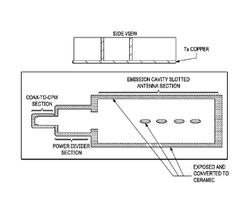
[0011] FIG. 2 shows a miniature air cavity slotted antenna.
[0012] FIG. 3 shows a cross section miniature air cavity slotted antenna.
[0013] FIG. 4A shows a prior art moderate size CNC machined metal air cavity
slotted
antenna.
[0014] FIG. 4B shows a prior art small CNC machined metal air cavity slotted
antenna.
[0015] FIGS. 5A to 5L show an example of a method for making a single wafer
slotted
waveguide antenna structure with matched ground plane and/or RF isolation
structure, and
FIG. 6L shows a cross-sectional view of the final matched ground plane and/or
RF isolation
structure.
[0016] FIGS. 6A to 61 show an example of a method for making a two wafer
slotted
waveguide antenna structure with matched ground plane and/or RF isolation
structure, and
FIG. 6J shows a cross-sectional view of the final, two wafer matched ground
plane and/or
RF isolation structure.
[0017] FIG. 7 is a flow chart of another method of the present invention for
making a slotted
waveguide antenna structure with matched ground plane and/or RF isolation
structure.
DETAILED DESCRIPTION OF THE INVENTION
[0018] While the making and using of various embodiments of the present
invention are
discussed in detail below, it should be appreciated that the present invention
provides many
applicable inventive concepts that can be embodied in a wide variety of
specific contexts.
The specific embodiments discussed herein are merely illustrative of specific
ways to make
and use the invention and do not delimit the scope of the invention.
[0019] To facilitate the understanding of this invention, a number of terms
are defined
below. Terms defined herein have meanings as commonly understood by a person
of
ordinary skill in the areas relevant to the present invention. Terms such as
"a", "an" and
"the" are not intended to refer to only a singular entity, but include the
general class of which
Date Recue/Date Received 2021-08-19
10a
a specific example may be used for illustration. The terminology herein is
used to describe
specific embodiments of the invention.
[0020] The present invention relates to creating a compact air cavity slotted
antenna with a
50 Ohm launch and mini coaxial cable connector. Compact low loss air cavity
slotted
antennae are critical elements for high efficiency RF communication systems.
Compact air
cavity slotted antenna is a cornerstone technological requirement for future
RF systems for
portable systems, base station, test equipment and point-to-point
communication.
[0021] Photosensitive glass structures have been suggested for a number of
micromachining
and microfabrication processes such as integrated electronic elements in
conjunction with
other elements systems or subsystems. Semiconductor microfabrication using
thin film
additive and subtractive processes on semiconductor, insulating or conductive
substrates is
expensive with low yield and a high variability in performance. This invention
provides a
cost effective glass ceramic air cavity slotted antenna device or as an array
of air cavity
slotted antenna for RF frequencies with low loss.
[0022] FIG. 1 shows a typical layout for a slotted antenna. FIG 2 shows a
miniature air
cavity slotted antenna. FIG 3 shows a cross section miniature air cavity
slotted antenna. FIG
4A shows a moderate size CNC machined metal air cavity slotted antenna. FIG 4B
shows a
Date Recue/Date Received 2021-08-19
11
small CNC machined metal air cavity slotted antenna. FIGS. 4A and 4B show a
classic air
cavity slotted antenna that could made using classic CNC machining. FIG. 2
shows the top
view of a theoretical structure for a compact air cavity slotted antenna.
FIGS. 3 shows the
cross section view of a theoretical structure for a compact air cavity slotted
antenna a
theoretical structure of a compact air cavity slotted antenna. The external
dimensions of the
compact air cavity slotted antenna are: 8 (1) x 5.0 (w) x 0.4 (h) mm3. FIGS.
4A and 4B
shows images of commercial slotted air cavity slotted antennas.
[0023] Traditional slotted air cavity slotted antenna use traditional
machining and finishing
techniques because of the relatively large spacing slotted air cavity antenna.
Traditional
slotted air cavity slotted antenna used precision machining metal and
electropolished for
surface finish easily produce and are self-supporting antenna due to the
thickness of the
metal structures. Thin film or additive/subtractive manufacturing technology
produce
resonate elements that are not mechanically or dimensionally stable. This
mechanical or
dimensional instability forced the use of a solid dielectric
substrate/cavities creating large
losses. This large amount of loss has precluded the development and production
of a slotted
air cavity antenna for commercial markets.
[0024] The width is a multiple of the free space wavelength of the emission
frequency. The
center-to-center spacing between the slots of 212.
[0025] The present invention includes a method to fabricate to compact slotted
air cavity
antenna photodefinable glass ceramic substrate. To produce the present
invention the
inventors developed a glass ceramic (APEX Glass ceramic) as a novel packaging
and
substrate material for semiconductors, RF electronics, microwave electronics,
and optical
imaging. APEX Glass ceramic is processed using first generation semiconductor
equipment
in a simple three step process and the final material can be fashioned into
either glass,
ceramic, or contain regions of both glass and ceramic. Photo-etchable glasses
have several
advantages for the fabrication of a wide variety of microsystems components.
Although the
current embodiment has been demonstrated in APEX glass due to it superior
processing
attributes but could be practice on other forms of photodefinable glass or by
additive and
subtractive thin film processes. The APEX glass approach has the lowest cost
highest
preforming slotted antennas.
[0026] Microstructures have been produced relatively inexpensively with these
glasses using
conventional semiconductor processing equipment. In
general, glasses have high
temperature stability, good mechanical and electrically properties, and have
better
Date Recue/Date Received 2021-03-11
12
chemical resistance than plastics and many metals. Photoetchable glass is
comprised of
lithium-aluminum-silicate glass containing traces of silver ions. When exposed
to UV-light
within the absorption band of ceriumoxide, the ceriumoxide acts as
sensitizers, absorbing a
photon and losing an electron that reduces neighboring silver oxide to form
silver atoms,
e. g. ,
3+ + 4+ 0
Ce +Ag = Ce +Ag
[0027] The silver atoms coalesce into silver nanoclusters during the baking
process and
induce nucleation sites for crystallization of the surrounding glass. If
exposed to UV light
through a mask, only the exposed regions of the glass will crystallize during
subsequent heat
treatment.
[0028] This heat treatment must be performed at a temperature near the glass
transformation
temperature (e.g., greater than 465 C. in air). The crystalline phase is more
soluble in
etchants, such as hydrofluoric acid (HF), than the unexposed dvitreous,
amorphous regions.
The crystalline regions etched greater than 20 times faster than the amorphous
regions in
10%HF, enabling microstructures with wall slopes ratios of about 20:1 when the
exposed
regions are removed. See T.R.Dietrichetal., "Fabrication Technologies for
Microsystems
utilizing Photoetchable Glass", Microelectronic Engineering 30,497 (1996).
[0029] In general, photoetchable glass and is composed of silicon oxide (SiO2)
of 75-85% by
weight, lithium oxide (Li2O) of 7-11% by weight, aluminum oxide (A1203) of 3-
6% by
weight, sodium oxide (Na2O) of 1-2% by weight, 0.2-0.5% by weight antimonium
trioxide
(5b203) or arsenic oxide (As203), silver oxide (Ag2O) of 0.05-0.15% by weight,
and cerium
oxide (Ce02) of 0.01- 0.04% by weight. As used herein the terms "APEX Glass
ceramic",
"APEX glass" or simply "APEX" is used to denote one embodiment of the glass
ceramic
composition of the present invention.
[0030] The APEX composition provides three main mechanisms for its enhanced
performance: (1) The higher amount of silver leads to the formation of smaller
ceramic
crystals which are etched faster at the grain boundaries, (2) the decrease in
silica content (the
main constituent etched by the HF acid) decreases the undesired etching of
unexposed
material, and (3) the higher total weight percent of the alkali metals and
boronoxide produces
a much more homogeneous glass during manufacturing.
[0031] The present invention includes a method for fabricating a low loss RF
Filter structure
in APEX Glass structure for use in forming interdigitated structures with
mechanical
Date Recue/Date Received 2021-03-11
13
stabilization and electrical isolation in a glass ceramic material used. The
present invention
includes metal structures to create in multiple planes of a glass-ceramic
substrate, such
process employing the (a) exposure to excitation energy such that the exposure
occurs at
various angles by either altering the orientation of the substrate or of the
energy source, (b) a
bake step and (c) an etch step. The slotted structures can be either symmetric
or asymmetric.
The mechanically stabilized structures are difficult, if not infeasible to
create in most glass,
ceramic, silicon substrates or other substrates. The present invention has
created the
capability to create such structures in both the vertical as well as
horizontal plane for glass-
ceramic substrates.
[0032] Ceramicization of the glass is accomplished by exposing a region of the
APEX Glass
substrate to approximately 20J/cm2 of 310nm light. In one embodiment, the
present
invention provides a quartz/chrome mask containing a variety of concentric
circles with
different diameters.
[0033] The present invention includes a method for fabricating a compact
efficient RF filters
using mechanically stabilized interdigitated resonate structures connect
different electronic
devices fabricated in or attached to the photosensitive glass. The
photosensitive glass
substrate can have a wide number of compositional variations including but not
limited to:
60 - 76 weight % silica; at least 3 weight % K20 with 6 weight % - 16 weight %
of a
combination of K20 and Na2O; 0.003-1 weight % of at least one oxide selected
from the
group consisting of Ag2O and Au20; 0.003-2 weight % Cu2O; 0.75 weight % - 7
weight %
B203, and 6 - 7 weight % Al2O3; with the combination of B203; and A1203 not
exceeding 13
weight %; 8-15 weight % Li2O; and 0.001 ¨ 0.1 weight % Ce02. This and other
varied
compositions are generally referred to as the APEX glass.
[0034] The exposed portion may be transformed into a crystalline material by
heating the
glass substrate to a temperature near the glass transformation temperature.
When etching the
glass substrate in an etchant such as hydrofluoric (HF) acid, the anisotropic-
etch ratio of the
exposed portion to the unexposed portion is at least 30:1 when the glass is
exposed to a
broad spectrum mid-ultraviolet (about 308-312nm) flood lamp to provide a
shaped glass
structure that have an aspect ratio of at least 30:1, and to provide a lens
shaped glass
structure. The exposed glass is then baked typically in a two-step process.
Temperature range
heated between of 420 C-520 C for between 10 minutes to 2 hours, for the
coalescing of
silver ions into silver nanoparticles and temperature range heated between 520
C-620 C for
between 10 minutes and 2 hours allowing the lithium oxide to form around the
silver
nanoparticles. The glass plate is then etched. The glass substrate is etched
in an etchant, of
Date Recue/Date Received 2021-03-11
14
HF solution, typically 5% to 10% by volume, where in the etch ratio of exposed
portion to
that of the unexposed portion is at least 30:1. Create the mechanically and
thermally
stabilized slot antenna resonate structure through thin film additive and
subtractive processes
requires the general processing approach.
[0035] There are multiple methods considered by the inventors to achieve a
slotted antenna
in photodefinable glass. One such embodiment uses a single wafer to create the
slotted
antenna. A second embodiment considered by the inventors uses a dual wafer
structure to
create the slotted antenna.
[0036] The present inventors used a photo-definable glass ceramic (APEX )
Glass Ceramic
or other photo definable glass as a novel substrate material for
semiconductors, RF
electronics, microwave electronics, electronic components and/or optical
elements. In
general, a photo definable glass is processed using first generation
semiconductor equipment
in a simple three step process and the final material can be fashioned into
either glass,
ceramic, or contain regions of both glass and ceramic to create a slotted
waveguide antenna
structure with a matched ground plane comprising: forming in a photosensitive
glass
substrate a coaxial-to-coplanar waveguide (CPW) section connected to a power
divider that
is connected to an emission cavity while retaining one or more solder bumps at
the vias that
connect to an integrated ground plane.
[0037] Single Wafer.
[0038] A single wafer method of making the slotted antenna section of a
compact slotted air
cavity antenna (CSACA) starts with a lap and polished photodefinable glass
substrate is
shown in FIGS. 5A to 5L. Where the substrate between 150 and 300 pm thick with
a
surface roughness less than or equal to 50nm and surface to surface parallel
less than or
equal to 10% with an RMS roughness < 100A.
[0039] On a backside of the lapped and polished photodefinable glass wafer
from, use a
photomask to image at 310 nm light at a at least an intensity of 2 J/cm2 to
expose the
sidewalls of the slotted antenna and support elements of the emission section
of the slotted
antenna.
[0040] The bottom of the substrate that has been coated with Ta and Copper.
Where Ta is
deposited by sputter deposition at a thickness between 50A and 750A preferably
250A.
Where the copper is deposited by electroplating deposition at a thickness
between 1pm and
100 p.m but preferably 30 p.m. There are many RF CSACA die on a single 6"
wafer. The
Date Recue/Date Received 2021-03-11
15
specific number of die per wafer is a function of the wafer diameter and CSACA
device
design.
[0041] The wafer is then coated with a photoresist and the via and ground
plane sidewall
pattern for the CSACA is exposed and developed. The substrate is 6" in
diameter is exposed
with approximately 20J/cm2 of 310nm light with a photo mask has a pattern of
through hole
via and ground plane sidewalls of the emission section CSACA device. The
through hole
via are between 30 [tin and 1201,t preferably 80 p.m in diameter with a center-
to-center
spacing between 2,000 p.m and 100 p.m preferably at a 500 tm center-to-center
spacing.
Where the ground plane sidewalls are between 500 p.m and 5 p.m preferably at a
50 mm
thick. The photoresist is then removed using a standard photoresist stripper.
[0042] The wafer is then annealed at temperature range heated between of 420 C-
520 C for
between 10 minutes to 2 hours, for the coalescing of silver ions into silver
nanoparticles and
temperature range heated between 520 C-620 C for between 10 minutes and 2
hours
allowing the lithium oxide to form around the silver nanoparticles. The wafer
is then cooled
and placed into an HF bath to etch the ceramic portion of the wafer.
[0043] Then the via and ground plane sidewalls are filled using a copper
electroplating
process. The copper electroplating process grows the via and ground plane
sidewalls from
the backside copper rough the substrate.
[0044] The contact area between via and bottom ground plane is about 5% of the
surface
area contact to the final metal CSACA structure. The greater the number of
stabilization
structures, the higher the RF losses. As such we elect not to make the
stabilization structure
greater than 50% of the contact area of the CSACA structure and preferably
less than 5%.
The front of the wafer is then planarized using a CMP process to remove any
excess copper.
[0045] The top of the is flood exposed with approximately 20J/cm2 of 310nm
lightõ The
wafer is then annealed at temperature range heated between of 420 C-520 C in
argon for
between 10 minutes to 2 hours, for the coalescing of silver ions into silver
nanoparticles and
temperature range heated between 520 C-620 C in argon for between 10 minutes
and 2
hours allowing the lithium oxide to form around the silver nanoparticles. This
enables the
formation of the ceramic phase of the photodefinable glass.
[0046] The wafer is then cooled and covered with a photoresist where it is
exposed with the
desired slot pattern for the CSACA using a standard photoresist process. This
leaves a
photoresist pattern where the slots will be in the CSACA. The wafer is placed
in a
sputtering chamber where a thin layer of Ta between 50A and 750A preferably
250A and a
Date Recue/Date Received 2021-03-11
16
seed layer of copper between 0.5 p.m and 5 p.m preferably 2 p.m of copper. The
substrate is
the placed into a photoresist stripper to leave the pattern of slots
surrounded and outlined by
a thin film of copper. The wafer is placed into a copper
electroplating/electroless plating
bath where an addition 15 p.m to 50 p.m preferably 25 p.m is deposited on
copper thin film.
The wafer is then placed in a 10% HF solution where the ceramic portion is
removed from
the emission sections cavity. The wafer is then placed in a DI water rinse to
neutralize/dilute
the HF fluid. Then the wafer is placed into, e.g., a Isopropyl Alcohol (IPA)
rinse to do a
fluid exchange with any water. The wafer is then placed into a vacuum bake
oven to remove
any residual IPA. The bake oven is at 40 C to 70 C at a preferably 50 C
pressure ranging
between 1 mtorr and 750 mtorr preferable 400 mtorr.
[0047] Processing the micro-coaxial cable to coplanar waveguide and power
divider section
are accomplished in a similar manner the emission section of the slotted
antenna. The first
processing step is to expose the interior of microcoaxial cable and power
divider sections of
the CSACA with a photo mask has a pattern of through hole via and ground plane
sidewalls
CSACA device.
[0048] The wafer is then placed into a copper electroplating bath where cooper
is deposited
at a thickness between 0.5 p.m and 10 p.m.
[0049] The ceramic portion of the exposed/converted glass is then etched away
using 10%
HF solution leaving the interdigitated, ground plane and input and output
structures. The
wafer is then rinsed and dried using DI water and IPA.
[0050] The wafer is then annealed at temperature range heated between of 420 C-
520 C for
between 10 minutes to 2 hours, for the coalescing of silver ions into silver
nanoparticles and
temperature range heated between 520 C-620 C for between 10 minutes and 2
hours
allowing the lithium oxide to form around the silver nanoparticles. The wafer
is then cooled
and placed into a 10% HF bath to etch the ceramic portion of the wafer. The
wafer is then
placed into a CVD deposition system for a deposition between 200 A and 10,000
A thick of
titanium. The wafer is then coated with a photoresist and the via pattern is
exposed and
developed. The wafer is then placed into a copper-electroplating bath where
between 25 m
and 35 p.m of copper are deposited. The photoresist is then removed lifting
off the majority
of the cooper and leaving the cooper filled via. The wafer is then lapped and
polished to
remove any excess copper and planarize the surface of the glass and cooper
filled via.
[0051] The wafer is then exposed with approximately 20J/cm2 of 310nm light to
a photo
mask consisting of a rectangular pattern of ¨5.3 mm by ¨2.2 mm. As can be seen
in FIG 7.
Date Recue/Date Received 2021-03-11
17
The wafer is then annealed, in Argon at temperature range heated between of
420 C-520 C
for between 10 minutes to 2 hours, for the coalescing of silver ions into
silver nanoparticles
and temperature range heated between 520 C-620 C for between 10 minutes and 2
hours
allowing the lithium oxide to form around the silver nanoparticles. The wafer
is then cooled.
A photoresist is then coated on the front of the wafer and the lid pattern is
exposed and
developed. The remaining photoresist covers the exposed and converted ceramic.
Both
sides of the wafer are coated with 200 A and 10,000 A thick of titanium using
CVD process.
The wafer is then placed into a copper-electroplating bath where cooper is
deposited at a
thickness between 0.5 p.m and 20 p.m. The photoresist is then removed lifting
off the
majority of the cooper and leaving the converted ceramic exposed and any
unwanted
remaining seed layer is removed using any number of well-established
techniques. The
ceramic portion of the exposed/converted glass is then etched away using 10%
HF solution
leaving the ground plane structures. The wafer is then rinsed and dried using
DI water and
IPA. Table 1 is a detailed step-by-step example of a protocol for
manufacturing the slotted
antenna using in a single wafer.
[0052] Table 1. A single wafer slotted waveguide antenna structure with
matched ground
plane and/or RF isolation structure is created creating by:
Step 1. Start with lapped and polished photodefinable glass preferably APEX
glass of
between 150 and 300 um thick with a surface roughness less than or equal to
50nm and surface to surface parallel less than or equal to 10% with an RMS
roughness < 100A. See FIG. 5A
Step 2. On backside of the photodefinable glass wafer from Step 1, use a
photomask
to image at 310 nm light at at least an intensity of 2 J/cm2 to expose the
sidewalls
and support elements of the structure.
Step 3. Thermal cycle above the glass transition temperature to convert the UV
exposed glass to ceramic phase for outside, inside walls and the via of the
entire
structure section.
Step 4. Uniformity deposit 250A of Ta and 2 p.m Copper by sputtering on the
front
side of the wafer/substrate.
Step 5. Coat the substrate with photoresist to interior of the coax to CPW and
power
divider section.
Step 6. Etch the sidewalls and via in the substrate in 10% HF.
Step 7. Electroplate the sidewalls and support via from the sputtered copper
layer.
Step 8. Apply a photoresist and using a photomask cover everything but the
coax to
Date Recue/Date Received 2021-03-11
18
CPW and power Divider sections.
Step 9. Exposing the photodefinable glass wafer image at 310 nm light at a at
least an
intensity of 2 J/cm2 to expose the emission cavity of the structure.
Step 10. Remove photoresist using a standard photoresist stripper.
Step 11. Using a different mask expose the coax to CPW and power
Divider
sections to an intensity of 2 J/cm2 to expose for approximately 50% of the
time.
Step 12. Remove photoresist using a standard photoresist stripper.
Step 13. Thermal cycle above the glass transition temperature covert
the UV
exposed glass to ceramic phase for of step 8 and Step 11. See FIG. 5B
Step 14. Coat the front of the wafer with photoresist exposing and
developing
the slots for the antenna by cover the slots regions with photoresist
Step 15. Deposit 250A of Ta and 2 um Copper by sputtering on the front
side
of the wafer/substrate on the center part of the antenna form Step 14.
Step 16. Remove photoresist
Step 17. Electroplate 20um of copper on both sides of substrate on top
of the
sputtered copper in Step 15.
Step 18. Coat the wafer with photoresist except for the field of the
slotted
antenna resonator cavity exposing the power divider and coax to CPW sections.
Step 19. Etch the substrate in 10% HF half way through the substrate
of the
ceramic phase material created in Step 11 and Step 13.
Step 20. Rinse the wafer with DI water. See FIG. 5C
Step 21 Using a projection aligner expose the region a pattern of
glass pillars
and pillar regions.
Step 22 Coat the wafer with a silver nitrate. Reduce the silver
nitrate using IR
source to produce a pattern of reduced silver on the power divider and coax to
CPW sections. See FIG. 5D
Step 23 Electroless plate copper on to the metallic silver
Step 24 Heat the structure to 250 C in argon to promote adhesion of
silver
copper structure. See FIG. 5E
Step 25 Using a spin on glass 5i02 lightly etch the using a standard
plasma
etching process to expose the copper sidevvalls around the power divider and
coax to CPW sections. See FIG. 5G
Step 26 Plasma etch down to the copper sidewalls.
Step 27 Coat the wafer with photoresist and open the region over the
spin on
Date Recue/Date Received 2021-03-11
19
glass over where the contact is the tab for power divider and coax to CPW
sections.
Step 28 Plasma etch down to the copper contact/tab.
Step 29 Remove the photoresist using a standard stripper the rinse
with DI
water
Step 30 Using a photoresist to coat the wafer clearing a pattern over
the power
divider sections.
Step 31 Sputter coat the wafer with 250A of Ta the 21,tm of Copper.
See FIG.
5H
Step 32 Electroless plate copper on the exposed sputtered copper to
20 um
See FIG. 51
Step 33 Remove Photoresist using a standard Photoresist stripper
Step 34 Rinse the wafer with DI water
Step 35 Deposit solder bump bond by an ink jet printer. This solder
bump is
to make contact with the center electrode of the micro coaxial connector to
the coax to CPW element. This solder ball may require repeated applications
to fill the by to the copper tab of the coax to CPW element.
Step 36 The wafer is the heat to allow the solder to flow making a
solid
electrical and mechanical connection to the tab of the coax to CPW element.
This is generally between 225 C and 235 C for 30 secs.
Step 37 Rinse the wafer in 10% HF, to remove all of the remain
ceramic
material and spin on glass from the cavity of the antenna.
Step 38 Rinse the wafer in DI water and the IPA. Vacuum dry the wafer
at
120 C at 1 torr for 1 hour.
Step 39 Deposit solder bump bond via an ink jet deposition process in
5 sites,
four sites on the perimeter to make contact the ground plane and attach the
micro coaxial connector to the substrate. The fifth solder bump is to make
contact with the center electrode of the micro coaxial connector to the coax
to
CPW element. This solder ball may require repeated applications to fill the
via to the copper tab of the coax to CPW element. See FIG. 5J
Step 40 Attach the commercially available surface mount micro coaxial
connector to the solder bumps See FIG. 5k
Step 41 Dice the wafer into individual die.
Date Recue/Date Received 2021-03-11
20
[0053] Two Wafer method.
[0054] A two wafer method of making the slotted antenna section of a compact
slotted air
cavity antenna (CSACA) starts with a lap and polished photodefinable glass
substrate is
shown in FIGS. 6A to 6J. Where the substrate between 150 and 300 pm thick with
a
surface roughness less than or equal to 50nm and surface to surface parallel
less than or
equal to 10% with an RMS roughness < 100A. Table 2 is one example of a two
wafer
transmission structure with matched ground plane and/or RF isolation
structure.
[0055] Table 2. In an example of Step-by-step method of making a slotted
antenna of the
present invention.
First Wafer
Step 1. Start with two lapped and polished photodefinable glass preferably
APEX glass
of between 150 and 150 um thick with a surface roughness less than or equal to
50nm and surface to surface parallel less than or equal to 10% with an RMS
roughness < 100A.
Place photoresist or wax on the substrate's topside.
Step 2. Expose the pattern to the right in the side one of the first wafer
glass wafer from
Step 1, use a photomask to image at 310 nm light at a at least an intensity of
2 J/cm2
to expose the emission cavity's sides and support elements of the structure.
Step 3. Thermally cycle the substrate to convert the exposed material to a
ceramic
Step 4. Coat the First/Top substrate with photoresist, expose and develop the
slots for
RF emissions in the form to the right.
Step 5. Expose and develop the pattern seen to the right into the substrates
of the top
substrate from step 4.
Step 6. Deposit 250A of Ta and lum of Copper by sputtering on the top of the
first
wafer.
Step 7. Electroplate 20um of copper
Step 8. Coat the front of the wafer with wax, photoresist or other protective
coating
Step 9. Etch the via and support structures created in Step 3 and Step 2.
Step 10. Electroplate the copper pillars and sidewalls from the copper
layer in
Step 7.
Step 11. CMP the backside to be flat from Step 10.
Step 12. Expose the cavity to the right in the side one of the first
wafer glass
wafer from Step 1, use a photomask to image at 310 nm light at a at least an
Date Recue/Date Received 2021-03-11
21
intensity of 2 J/cm2 to expose the emission cavity, power divider and coax to
CPW
sections.
Step 13. Thermally cycle the substrate to convert the exposed material
to a
ceramic phase from the exposure in Step 12. This will be etched after the two
wafers have been bonded together.
Second Wafer
Step 1 On the front surface of the 2nd wafer in the micro coaxial connector
and power
divider section use a photo mask to shield the areas that are identified as
glass. Use
310 nm light at a at least an intensity of 2 J/cm2 to expose the emission
cavity's
sidewalls and support elements structure.
Step 2 Thermally cycle the substrate to convert the exposed material to a
ceramic phase
in Step 1.
Step 3 Coat the First/Bottom substrate with photoresist expose and develop the
pattern
seen to the right into the substrate's bottom side of the top substrate
creating a
pattern for the external copper slotted antenna. See the second figure.
Step 4 Deposit 250A of Ta and lum of Copper by sputtering on the top of the
first
wafer.
Step 5 Remove the photoresist using a standard stripper
Step 6 Electroplate 20um of copper
Step 7 Coat the backside of the wafer with wax, photoresist or other
protective coating
from Step 6.
Step 8 Etch the sidewalls and support pillar ceramic phase out created in Step
2 and
Step 1.
Step 9 Electroplate copper pillars and sidewalls from the copper on the front
side of the
second wafer
Step 10 Rise with DI water and dry
Step 11 CMP the backside to be flats
Step 12 On the front surface of the 211d wafer in the micro coaxial
connector
power divider section use a photo mask to shield the areas that are identified
as
glass. Seen to the Right. At the same time accomplish a flood expose antenna
emission section. Use 310 nm light at a at least an intensity of 2 J/cm2.
Step 13 Thermally cycle the substrate to convert the exposed material
to a
ceramic phase in Step 1.
Step 14 Deposit a photoresist on the front surface, using a mask
create the image
Date Recue/Date Received 2021-03-11
22
identified in light grey by exposing that pattern into the photoresist.
Step 15 Then sputter deposit 250A of Ta and 2 p.m of Copper.
Step 16 Remove photoresist using a standard photoresist stripper
leaving the
pattern in light grey.
Step 17 Deposit 20 p.m of copper using a electroless plate process
Step 18 Place solder balls on the on the copper elements of the front
surface of
the first wafer
Step 19 Accomplish wafer-to-wafer bonding using alignment fiducials
and
etched keyed structures.
Step 20 Keep the wafers in compression and wafer is the heat them to
allow the
solder to flow making a solid electrical and mechanical connection to the tab
of
the coax to CPW element. This is generally between 225 C and 235 C for 30
secs.
Step 21 Coat the joined substrates with photoresist exposing the slot
patterns
Coat the back side with wax or other material to protect the structure
Place the joined wafer into 10% HF to etch the exposed substrate through the
slots using to remove the ceramic phase from the resonator, power divider and
coax to CPW sections.
Rinse with DI water
Remove Photoresist using a standard Photoresist stripper
Rinse with DI water
Place substrate into a vacuum bake oven to remove any remaining fluid from the
internal sections of slotted antenna.
Step 22 Coat the substrate with photoresist exposing the slot
patterns
Etch the exposed substrate through the slots
Rinse with DI water
Remove Photoresist using a standard Photoresist stripper
Rinse with DI water
Place substrate into a vacuum bake oven to remove any remaining fluid from the
internal sections of slotted antenna
Step 23 Cross Section View of the cavity
[0056] FIG. 7 shows a flowchart 100 of the method of the present invention, in
which Step
102 includes make a ceramic for outside and inside via in the cavity section.
Next, in step
104, bake the vias. In step 106, etch the vias. In step 108, Pattern cavity at
100% intensity
Date Recue/Date Received 2021-03-11
23
and pattern CPW area at 50%, bake, no etch at this time. In step 110, pattern
the backside
metal for the ground plane. In step 112, plate though glass and polish topside
to remove
overburden. In step 114, pattern topside metal and plate thick conductive
metal (e.g.,
copper) with slots. And in step 116, etching out the cavity to form the
slotted antenna in a
single wafer.
[0057] It is contemplated that any embodiment discussed in this specification
can be
implemented with respect to any method, kit, reagent, or composition of the
invention, and
vice versa. Furthermore, compositions of the invention can be used to achieve
methods of
the invention.
[0058] It will be understood that particular embodiments described herein are
shown by way
of illustration and not as limitations of the invention. The principal
features of this invention
can be employed in various embodiments without departing from the scope of the
invention.
Those skilled in the art will recognize, or be able to ascertain using no more
than routine
experimentation, numerous equivalents to the specific procedures described
herein. Such
equivalents are considered to be within the scope of this invention.
[0059] All publications and patent applications mentioned in the specification
are indicative
of the level of skill of those skilled in the art to which this invention
pertains.
[0060] The use of the word "a" or "an" when used in conjunction with the term
"comprising" herein may mean "one," but it is also consistent with the meaning
of "one or
more," "at least one," and "one or more than one." The use of the term "or" in
the claims is
used to mean "and/or" unless explicitly indicated to refer to alternatives
only or the
alternatives are mutually exclusive, although the disclosure supports a
definition that refers
to only alternatives and "and/or." Throughout this application, the term
"about" is used to
indicate that a value includes the inherent variation of error for the device,
the method being
employed to determine the value, or the variation that exists among the study
subjects.
[0061] As used herein the words "comprising" (and any form of comprising, such
as
"comprise" and "comprises"), "having" (and any form of having, such as "have"
and "has"),
"including" (and any form of including, such as "includes" and "include") or
"containing"
(and any form of containing, such as "contains" and "contain") are inclusive
or open-ended
and do not exclude additional, unrecited elements or method steps. In
embodiments of any
of the compositions and methods provided herein, "comprising" may be replaced
with
"consisting essentially of' or "consisting of'. As used herein, the phrase
"consisting
essentially of' requires the specified integer(s) or steps as well as those
that do not materially
Date Recue/Date Received 2021-08-19
24
affect the character or function of the claimed invention. As used herein, the
term
"consisting" is used to indicate the presence of the recited integer (e.g., a
feature, an element,
a characteristic, a property, a method/process step or a limitation) or group
of integers (e.g.,
feature(s), element(s), characteristic(s), property(ies), method/process steps
or limitation(s))
only.
[0062] The term "or combinations thereof' as used herein refers to all
permutations and
combinations of the listed items preceding the term. For example, "A, B, C, or
combinations
thereof' is intended to include at least one of: A, B, C, AB, AC, BC, or ABC,
and if order is
important in a particular context, also BA, CA, CB, CBA, BCA, ACB, BAC, or
CAB.
Continuing with this example, expressly included are combinations that contain
repeats of
one or more item or term, such as BB, AAA, AB, BBC, AAABCCCC, CBBAAA,
CABABB, and so forth. The skilled artisan will understand that typically there
is no limit on
the number of items or terms in any combination, unless otherwise apparent
from the
context.
[0063] As used herein, words of approximation such as, without limitation,
"about",
"substantial" or "substantially" refers to a condition that when so modified
is understood to
not necessarily be absolute or perfect but would be considered close enough to
those of
ordinary skill in the art to warrant designating the condition as being
present. The extent to
which the description may vary will depend on how great a change can be
instituted and still
have one of ordinary skill in the art recognize the modified feature as still
having the
required characteristics and capabilities of the unmodified feature. In
general, but subject to
the preceding discussion, a numerical value herein that is modified by a word
of
approximation such as "about" may vary from the stated value by at least 1,
2, 3, 4, 5, 6, 7,
10, 12 or 15%.
[0064] All of the compositions and/or methods disclosed herein can be made and
executed
without undue experimentation in light of the present disclosure. While the
compositions
and methods of this invention have been described in terms of preferred
embodiments, it will
be apparent to those of skill in the art that variations may be applied to the
compositions
and/or methods and in the steps or in the sequence of steps of the method
described herein
without departing from the scope of the invention.
Date Recue/Date Received 2021-08-19