Note: Descriptions are shown in the official language in which they were submitted.
CA 03113121 2021-03-17
WO 2020/058332 PCT/EP2019/075000
1
Antifouling system with inductive power transfer for use in protecting a
surface against
biofouling.
FIELD OF THE INVENTION
The present disclosure relates to antifouling systems having inductive power
transfer systems for powering a load of the antifouling system. The disclosure
further
relates to an object subject to fouling when in use and having such
antifouling system.
BACKGROUND OF THE INVENTION
Biofouling or biological fouling is the accumulation of microorganisms,
plants, algae, and/or animals on surfaces and especially those that are
exposed to moist or
watery environment such as sea, lake or river. The variety among biofouling
organisms is
highly diverse and extends far beyond attachment of barnacles and seaweeds.
According to
some estimates, over 1700 species comprising over 4000 organisms are
responsible for
biofouling. Biofouling is divided into microfouling which includes biofilm
formation and
bacterial adhesion, and macrofouling which is the attachment of larger
organisms. Due to
the distinct chemistry and biology that determine what prevents organisms from
settling,
these organisms are also classified as hard or soft fouling types.
Calcareous (hard) fouling organisms include barnacles, encrusting
bryozoans, mollusks, polychaete and other tube worms, and zebra mussels.
Examples of
non-calcareous (soft) fouling organisms are seaweed, hydroids, algae and
biofilm "slime".
Together, these organisms form a fouling community.
In several circumstances, biofouling creates substantial problems such as for
example . Machinery stops working, water inlets get clogged, and hulls of
ships suffer
from increased drag and thus increased fuel consumption. It is estimated that
an increase of
up to 40% in fuel consumption can be attributed to biofouling. As large oil
tankers or
container transport ships can consume up to Ã200,000 a day in fuel,
substantial savings are
possible with an effective method of antifouling. Hence the topic of
antifouling, i.e. the
process of removing or preventing fouling from forming, is well known.
In industrial processes, bio-dispersants can be used to control biofouling. In
less controlled environments, organisms are killed or repelled with coatings
using biocides,
CA 03113121 2021-03-17
WO 2020/058332 PCT/EP2019/075000
2
thermal treatments or pulses of energy. Nontoxic mechanical strategies that
prevent
organisms from attaching include choosing a material or coating with a
slippery surface, or
creation of nanoscale surface topologies similar to the skin of sharks and
dolphins which
only offer poor anchor points.
WO 2014/188347 discloses a system for preventing biofouling in which all
of a surface, or a significant amount of a surface, to be kept clean from
fouling (e.g. the
hull of a ship) is covered with a layer that emits germicidal light, in
particular UV light.
Thus, it is known to adopt a light based method, in particular using ultra-
violet (UV) light
to reduce or prevent fouling. It is well-known that most micro-organisms are
killed,
rendered inactive or unable to reproduce with sufficient UV light. This effect
is mainly
governed by the total dose of UV light. A typical dose to kill 90% of a
certain micro-
organism is 10 mW-hours per square meter. A particularly effective type of
light in this
respect is UVC light with a wavelength in the approximate wavelength range of
100 to 280
nm. In WO 2014/188347 lower power UV LEDs are used to provide the necessary UV
light. LEDs can generally be included in small packages and consume less power
than
other types of light sources. LEDs can be manufactured to emit (UV) light of
various
desired wavelengths and their operating parameters, most notably the output
power, can be
controlled to a high degree. A suitable germicidal dose can easily be achieved
with existing
UV LEDs.
SUMMARY OF THE INVENTION
In the know system it is necessary to deliver power to the light sources
disposed in the layer applied to the ship. This is problematic in the sense
that the system
needs to be designed so that it allows application to a large irregularly
shaped surface of an
object (e.g. a ships hull) and is operable in conditions where it is at least
partly submerged
in water potentially giving rise to electrical hazards as well as issues of
corrosion.
There is therefore a need for an improved antifouling system that is
electrically powered.
It is an object of the invention to at least partly foresee in the
aforementioned need.
CA 03113121 2021-03-17
WO 2020/058332 PCT/EP2019/075000
3
It was realized by the inventors that the aforementioned conditions under
which such system must be applied and operated require a number of design
choices to be
made in order to cope with such conditions. A single element system with
protected
galvanic power provision circuitry would be preferred. But such system will be
really
.. difficult to design and mount to a large object.
According to a first aspect of the invention there is provided an antifouling
system as defined in the claims.
The inventors have recognized that an antifouling system with a modular
design including multiple antifouling panels for covering an area of a surface
of an object
would at least partly fulfill the aforementioned object. In particular this
would allow to cover
a large surface of an object (e.g. a ship's hull) by applying the antifouling
panels to different
areas of such surface. This will not only make mounting of the system easier,
but will make
the system more flexible in terms of shape (e.g. curved) and sizes of surfaces
that can be
covered. In order to make such a system a robustly operating one, the power
provision
strategy was chosen to be partly based on wireless power transfer with the
power
transmission system as defined in the claims. With such transfer system a
central power
inductive power emitter may be used to provide power to multiple inductive
power receivers.
Thus each panel can have one such receiver and thus be powered by the central
inductive
power emitter. This provides an effective way to deliver power to a load
(plurality of
antifouling devices) which extends over a large area. In particular, a grid of
at least one and
preferably more power delivery transmitters each one associated with multiple
power
receiving panels may be formed, to cover a large area. The inductive power
receivers and
transmitter(s) may be encapsulated in panels so that they are protected
against the
environmental conditions (e.g. water). Thus corrosion problems may be reduced
while power
can be transferred as needed. Furthermore, central power provision from a
power source (e.g.
ships generators or batteries or the like) to the inductive power emitter(s)
may be established
above the waterline of the object, so that galvanic connections may be used
for this purpose
without introducing e.g. problems of corrosion, while power transfer below the
waterline
can occur wirelessly. The use of wireless power transfer using inductive
elements such as
.. coils not only simplifies making a watertight arrangement by encapsulation
with no openings
to the environment, but also makes application of the antifouling system
easier. After all,
slight differences in alignment of emitter and receiver elements of different
across a
CA 03113121 2021-03-17
WO 2020/058332 PCT/EP2019/075000
4
generally irregular surface of an object, which would otherwise lead to
differences in power
transfer, can be tolerated to some extent with such inductive design.
With the power transfer system, the antifouling devices can be provided with
power to be driven to provide the antifouling radiation. The driving need not
be continuous
during use of the antifouling system. The driving may be periodic. In some
embodiments all
of the transferred power is used for this driving. In other embodiments only
part of this power
is used to drive the antifouling devices. Thus in such cases there may be more
power
transferred than needed for the driving of the antifouling devices. Hence
other devices, such
as sensors or data transfer devices may be driven using the excess power. In
variations to
these embodiments, the power may be used to drive the antifouling devices
discontinuously,
i.e. during one time period, while they are not driven (or at lower power
level) at another
time period different from the one time period. In this non-driven period
power may either
cease to be transferred or it may be used for driven other devices such as
sensors or data
transfer systems. Such may be convenient for example when there is not enough
power
transferred for driving all power requiring devices at the same time.
Preferably the antifouling devices of the antifouling system comprise UV
light sources and in particular comprise UV-C light sources. In such cases the
UV or UV-C
light provides the antifouling radiation.
The antifouling system is a modular system made of inductive power emitters
and inductive power receivers physically separated from each other in which
multiple
receivers may be provided with power by one emitter.
In an embodiment the antifouling system comprises a first panel (power
provision panel) including the inductive power emitter and a plurality of
second panels
(antifouling panels), separate from the first panel, each second panel
comprising at least one
of the plurality of inductive power receivers and at least one of the
plurality of antifouling
devices. The antifouling panels may cover a larger area than the power
provision panels. In
particular, each antifouling panel distributes the power received from the
power provision
panels to the antifouling devices within an antifouling panel. These devices
if there are more
than one are preferably distributed across the area of the antifouling panel.
Each one of the plurality of second panels preferably includes one or more
water resistant materials by which any of the plurality of inductive power
receivers and any
of the plurality of the antifouling devices present within that particular
second panel are
CA 03113121 2021-03-17
WO 2020/058332 PCT/EP2019/075000
encapsulated. The encapsulation serves to protecting the plurality of
inductive power
receivers and the plurality of antifouling devices against at least liquid
water. Protection
entails at last partial but preferably entire shielding from environmental
water such as sea
water. This may reduce corrosion and short circuit problems of the receivers
and antifouling
5 devices when the system is used in watery conditions, after all they are
electrical devices
susceptible to such deteriorations. One example of water resistant materials
comprise
silicone polymers. Another comprises fluoroethylene polymers (FEP). The
encapsulation
may take many forms, one of which is comprises the devices embedded in at
least one of the
materials. The material may be one single type of material, but may also be a
composite in
mixed form or in layered form or both. There may thus be a system of layers
for example
comprising silicone polymers and FEP polymer. The devices may then be embedded
in the
silicone polymers while the FEP polymer serves as a further cover layer on top
of the silicone
polymer.
In an embodiment of the antifouling system the one or more inductive emitter
elements each comprise or consist of power emitter coils and the one or more
inductive
receiver elements each comprise or consist of power receiver coils and the
inductive power
emitter and the inductive power receivers are configured such that each one of
the one or
more power receiver coils at least partly overlaps with at least one of the
one or more power
emitter coils when the system is mounted to the object. Coils can serve as
efficient power
transfer elements providing an internal (enclosed) cross sectional area in
which magnetic
field flux is concentrated to be used for inductive coupling. A coil may have
one or more
windings such as for example more than 2, more than 3, more than 5 windings.
An emitter
coil may have less or more windings than a receiver coil. A coil (emitter
and/or receiver
coil) may have a core for further concentrating magnetic flux, but this is not
needed per se.
Emitter coil and receiver coil may have a same cross sectional area or
different cross
sectional area. For example an emitter coil may have a larger cross sectional
area than a
receiver coil. This is for example advantageous when multiple receiver coils
need to draw
power from one and the same emitter coil.
In an embodiment each one of the plurality of inductive power receivers are
configured such that the at least one power emitter element of a respective
inductive power
receiver element at least partly overlaps with the at least one power emitter
element when
the system is mounted to the object and wherein each one of the plurality of
second panels
CA 03113121 2021-03-17
WO 2020/058332 PCT/EP2019/075000
6
comprises one or more edge regions in which its at least one power receiver
element is
disposed. This overlap is advantageous for optimizing the inductive coupling.
Preferably any
emitting or receiving elements are then coils as disclosed herein before or
herein after. In
case there are second panels comprising the inductive power receivers each one
of the
plurality of second panels comprises one or more edge regions (22) in which
its at least one
power receiver element is disposed. Each of the secondary panels are for
example mounted
over the inductive power emitter. The inductive power emitter is for example
for mounting
over the surface of the object and the inductive power receiver panels overlap
the inductive
power emitter. Thus, the power receiver elements, for example in the form of
coils, take up
a relatively small area of the panels and the overlap areas of panels with
inductive power
transmitter parts only needs to be small so that the overall system may
generally be kept thin.
Also the area inductive power transmitters take up, for example when part of a
primary panel,
may be kept small in relation to the area covered by secondary panels.
The inductive power transmitter can comprise a power feed line and a power
return line for electrically connecting to the at least one power emitter
element. A pair of
power feed line and power return line may be referred to as a power
transmission line. The
inductive power emitter can be designed with a low AC transmission line
impedance leading
to low losses. Such line is referred to as partially or entirely balanced
transmission line. To
this end, the power feed line and return line may run side by side at defined
constant distance
along the lines with an isolator in between. They may be arranged side by side
in a single
layer multi conductor track setup or be arranged one on top of the other in a
multi conductor
layer setup. The latter may provide a nearly complete balancing of the power
transmission
line.
In an advantageous embodiment of the antifouling system the at least one
inductive emitter elements comprises a plurality of inductive emitter elements
each one
electrically connected in parallel configuration to the power feed line and to
the power return
line and positioned in series with respect to each other within the inductive
power emitter,
each one of the plurality of inductive emitter elements being arranged to
inductively couple
to at least one of the at least one inductive receiver elements of one of the
plurality of
inductive power receivers. Again the emitter and receiver elements preferably
are coils as
defined herein after or before. Each inductive power receiver may be
inductively coupled to
at least one and preferably one of the power emitter elements of the inductive
power emitter.
CA 03113121 2021-03-17
WO 2020/058332 PCT/EP2019/075000
7
Positioned in series means that the elements are spatially distributed in a
side by side fashion
with respect to each other such that there is at least some non-overlapping
part. This is a way
to deliver current to each power receiver element in an efficient way such
that power receiver
elements can be located side by side in an optimum alignment for covering a
large surface
of an object. Such system may be voltage driven. The use of emitter elements
in series (which
would mean the same current at all points) would make it more difficult to
maintain a total
voltage within a safety voltage limit, such as 50Vrms.
The inductive power emitter may have a power feed line extending from one
end of the inductive power transmitter to the at least one inductive emitter
element and a
power return line extending from the at least one inductive emitter element to
the one end of
the inductive power transmitter, wherein the power feed line and the power
return line are
located on one side of the at least one inductive emitter elements. Thus, for
each one of a
plurality of inductive emitter elements, the power feed line and the power
return line are
located on one side of such inductive power emitter. Preferably the lines run
along the same
side of the plurality of inductive power transmitters. In this way, the
magnetic fields caused
at the location of an inductive emitter element by the power feed line and
power return line,
which fields are of different strengths along the length of these lines as a
result of the tapping
off of current of successive coils due to the parallel electrical
configuration) are at least
partially or substantially cancelled, so that a more uniform magnetic field
strength is
achieved going from one inductive emitter element to another within an
inductive power
emitter.
In another arrangement of the antifouling system the inductive power emitter
comprises at least one inductive emitter element for inductive coupling to a
plurality of
power receiver elements, the plurality of power receiving elements being
comprised of the
at least one power receiver elements of at least two of the plurality of
inductive power
receivers. Preferably the inductive power emitter comprises a single inductive
emitter
element for coupling to each and every one of the power receiver elements of
the plurality
of inductive power receivers. Thus, a single power emitter element is used to
inductively
couple to a set of inductive power receivers. In this way, the inductive
coupling and therewith
power transfer to each inductive power receiver may be the same or close to
the same.
In an embodiment of the antifouling system the inductive power emitter
includes a power feed line and a power return line and each one of the at
least one inductive
CA 03113121 2021-03-17
WO 2020/058332 PCT/EP2019/075000
8
emitter elements comprises a section of the power feed line and a section of
the power return
line. No actual coils are now present but merely sections of the lines that
are near each other
to provide a sum field in between that can be used to inductively couple with
a power receiver
element. This is a simpler design.
In an embodiment of an antifouling system the system further comprises a
further one of the inductive power emitter and at least one connection member
wherein the
power feed line of the inductive power emitter is connected to the power
return line of the
further inductive power emitter via the connection member. In such an
arrangement, the
system comprises a set of inductive power emitters and each one is associated
with a
respective plurality of inductive power receivers. Each of the inductive power
transmitters
comprises a power feed line and a power return line and the power feed line of
one of the
inductive power emitters is connected to the power return line of the further
one of the
inductive power transmitters.
In this design, the individual inductive power transmitters do not have a
closed power transmission line. Instead, they define one half of one power
emitter coil and
one half of another power emitter coil. There is again one power emitter coil
which extends
over the full length of the strip.
Connecting members are then preferably provided between the second ends
of, for example, adjacently arranged inductive power emitters, to connect the
power feed
line of one transmitter with the power return line of an adjacent one to one
side and to connect
the power return line of said one transmitter with the power feed line of an
adjacent strip to
the other side.
The inductive power emitter may comprise a ferrite material for example in
the form of layer or sheet below the inductive emitter elements, hence between
the surface
of an object and the elements when the system is mounted to the object. The
system
efficiency can thus be kept high, e.g. close to 50% even if the surface over
which the system
is to be mounted is electrically conductive such as e.g. is the case with a
ships metal hull.
The ferrite material is between the surface, e.g. a ship's hull, and the
inductive transformer
primary windings, to prevent Eddy currents through the conductive layer which
defines the
surface. Such ferrite material may be dispensed with when the surface is made
of non-
conducting materials such as wood or plastic.
CA 03113121 2021-03-17
WO 2020/058332 PCT/EP2019/075000
9
A coating or paint material may be provided for application to the surface,
such that the system is for mounting over a layer of the coating or paint
material, wherein
the coating or paint material has a relative permeability (iLtr) greater than
20, for example
greater than 100, for example greater than 200. The coating or paint material
preferably is
thus located between the system and the surface.
The purpose is to prevent or attenuate the existence of Eddy currents in the
hull that will lead to losses. The higher the value the better the
performance. This
improves the coupling factor for example even if a polyester or aluminum hull
is used.
The high relative permeability for example may also give rise to a high
dielectric permittivity.
This provides an alternative way to reduce Eddy currents in the metal hull
(giving rise to losses) and may avoid the need for a ferrite material. The
coating or paint
material for example has embedded ferromagnetic particles.
The inductive power receivers for example have a thickness of less than 5
mm, for example less than 4 mm, for example less than 3 mm. This thickness
typically
includes a printed circuit board (PCB).
The secondary panels including the inductive power receivers may have
thickness of less than 2 cm, for example less than 1,5 cm or even less than 1
cm. This may
include the encapsulating material defined herein before.
The plurality of antifouling devices for example comprises one or more light
sources for providing antifouling light as described herein before. The
inductive power
transfer system may thus be part of a light based antifouling system to be
applied to the
surface. The light sources may be part of a light source arrangement for
example comprising
an array of UV-C LEDs for emitting UV light with a wavelength between 270nm
and 280nm.
The antifouling system can comprise a power source for delivering power to
the inductive power emitter. The power source for example comprises a resonant
circuit with
a resonant frequency of 50kHz to 1MHz, for example 50kHz to 200kHz, for
example 60kHz
to 90kHz.
The inductive power receivers and the inductive power transmitters may be
comprised in respective first and second panels each of these including a
silicone material
having a protective function and optionally also an optical function, e.g.
light guiding.
CA 03113121 2021-03-17
WO 2020/058332 PCT/EP2019/075000
A second panel may have many shapes such as triangular or rectangular. They
may have an area of 0.5 m2 or larger. Preferably they have an area of 2.5 m2
or larger. The
sides of such panels may be of dimensions (length and width) larger than 0.1
or 0.2 meter,
preferably larger than 0.5 meter. Not all sides of a panel, or of different
panels in case there
5 are more in a system, need to have the same dimensions.
The shapes and sizes (area) or dimensions (length, width) of the first panels
may be any as long as suitable for use in an antifouling system to be able to
protect ore even
cover the surface. They shapes and sizes may be chosen according to size and
shape of the
surface they need to be applied to. Since the surface preferably is one of a
marine object such
10 as vessel, ship etc., such surfaces are in general quite large, i.e.
larger or much larger than 1
m2
The first panel and therewith the inductive power transmitter may have any
shape, but preferably is elongate and more preferably is also rectangular. It
preferably has a
length larger than 0.2 meter, or larger than 0.5 meter. Even more preferable
is a length larger
than 1 meter. The width of a first panel may be any dimension as long as its
electrical
components can be housed. They could have a width of 0.1 meter or larger such
as for
example 0.5 meter or larger.
The system as described herein before is intended to be mounted to an
object that under normal use conditions is exposed to fouling. This in general
means that
also the system will be exposed to such conditions at least partially.
In a further aspect of the invention there is thus provided an object exposed
to fouling conditions when in normal use, the object comprising an antifouling
system as
described herein before wherein the inductive power emitter and the plurality
of inductive
power receivers are mounted on the object in a fixed configuration with
respect to each
other thereby to provide the inductive coupling. Fixed configuration means
that during use
of the object the parts of the system are not displaceable. This does not mean
that they
cannot be removed from the object such as for example would occur during
repair or
replacement of parts of the system. Fixation can be done in many ways such as
for example
with screws, clamps or gluing of any kind.
Each one of the plurality of antifouling devices preferably comprises a UV
light source for providing UV light as the antifouling radiation. The UV light
works on DNA
CA 03113121 2021-03-17
WO 2020/058332 PCT/EP2019/075000
11
level of the microorganisms and the system based on such sources may thus work
for a wide
variety of antifouling.
In an embodiment of the object the antifouling system comprises
- a first panel including the inductive power emitter (10) and
- a plurality of second panels, separate from the first panel, each second
panel
comprising at least one of the plurality of inductive power receivers (20) and
at least one of
the plurality of antifouling devices,
wherein the first panel and the plurality of second panels are mounted to the
object such that different ones of the plurality of second panels are mounted
at least partially
to different areas of the object. The modularity of the system allows covering
of the area of
the object to which the system is mounted such that first and second panels
are fixed to the
object next to each other to cover a large area while power can be efficiently
provided by a
first panel to multiple second panels. The first panels preferably have an
elongate shape for
this purpose where second panels extend laterally from the elongate shape
along the length
direction to form a scheme such as herring bone.
In an embodiment the object is for partial or complete submersion in water
when in normal use and wherein each one of the plurality of second panels
includes one or
more water resistant materials by which any of the plurality of inductive
power receivers and
any of the plurality of the antifouling devices present within that particular
second panel are
encapsulated for protecting them against water. The object preferably is one
that during use
is exposed to water and especially sea water. Such objects include for example
buildings
such as sluices, oil drilling platforms, pumping stations or buoys and vessels
such as ships.
A marine object may be any object as described hereinbefore or hereinafter
such as for
example a vessel or ship. Preferably the object is a ship. In all cases the
system is mounted
to the outside surface of the object such that at least the inductive power
receivers (or the
second panels they are part of) are mounted to this surface. Preferably also
the inductive
power emitters (or the first panels they are part of) are mounted to the
outside surface.
In an embodiment the object has a waterline and a part of the first panel is
mounted such that it remains above the waterline when the object is in use so
that a power
source for providing power to the inductive power emitter can be connected to
the inductive
power transmitter via a galvanic connection disposed above the waterline. The
power source
may be configured to provide the power to the inductive power emitter via a
galvanic
CA 03113121 2021-03-17
WO 2020/058332 PCT/EP2019/075000
12
connection disposed above the waterline of the marine object. The inductive
power emitter,
preferably in the form of a strip as discussed above, may extend to above the
waterline so
that a galvanic contact may be made to the power source at a location outside
the water, and
the system can be fully enclosed and encapsulated below the waterline when it
comes to the
power provision of the load.
Thus the object comprises a surface and the antifouling system is mounted
over the surface.
The object may have a coating material as defined herein above applied to its
surface and between its surface and the antifouling system. This is
advantageous for objects
made of conductive materials near the surface such as ships with a metal hull
or other
constructions as defined herein that have metal parts near the surface to
which the system is
applied.
The invention also provides a method of mounting an antifouling system as
disclosed to an object. Any of the features of the antifouling system and/or
object may be
used to define such method of mounting. For example there may be a method of
mounting
wherein at least part of the system and in particular an inductive power
emitter is mounted
above the waterline of an object. In an embodiment there may be applied a
ferrite material
and/or coating material with permittivity higher than 20 between the object
and at least the
inductive power transmitter.
These and other aspects of the invention will be apparent from and elucidated
with reference to the embodiment(s) described hereinafter.
BRIEF DESCRIPTION OF THE DRAWINGS
For a better understanding of the invention, and to show more clearly how it
may be carried into effect, reference will now be made, by way of example
only, to the
accompanying schematic drawings, in which:
Figure 1 shows an antifouling system of the invention applied to a ship for
protecting the surface of the ship in contact with water, i.e. the hull
surface;
Figure 2 shows a cross section (in a horizontal plane) of the system of
Figure 1 through the inductive power emitters, panels and part of the ship's
surface;
Figure 3 shows the coil arrangements in more detail;
CA 03113121 2021-03-17
WO 2020/058332 PCT/EP2019/075000
13
Figure 4 shows an example of the structure of the panel;
Figure 5 shows one possible electrical configuration of the primary and
power receiver coils;
Figure 6 shows a first way of arranging power emitter coils and power
transmission line within an inductive power emitter;
Figure 7 shows a second way of arranging power emitter coils and power
transmission line within an inductive power emitter;
Figure 8 shows a third way of arranging a power emitter coil using power
feed line and power return line of an inductive power emitter;
Figure 9 shows a way of arranging a power return line of one inductive
power emitter and a power feed line of another inductive power emitter such
that they
together form a inductive emitter element; and
Figure 10 shows an arrangement in which the inductive power emitter and
inductive power receiver panels are provided over a high magnetic permeability
paint
layer.
DETAILED DESCRIPTION OF THE EMBODIMENTS
Examples of the antifouling system as defined by the claims will be
described with reference to the Figures.
It should be understood that the detailed description and specific examples,
while indicating exemplary embodiments of the apparatus, systems and methods,
are
intended for purposes of illustration only and are not intended to limit the
scope of the
invention. These and other features, aspects, and advantages of the apparatus,
systems and
methods of the present invention will become better understood from the
following
description, appended claims, and accompanying drawings. It should be
understood that
the Figures are merely schematic and are not drawn to scale. It should also be
understood
that the same reference numerals are used throughout the Figures to indicate
the same or
similar parts.
Figure 1 shows such an antifouling system mounted to an object in the form
of a ship 1. The system is for protecting the object against fouling when the
ship is used.
This means that the system is at least capable of reducing fouling compared to
a ship
CA 03113121 2021-03-17
WO 2020/058332 PCT/EP2019/075000
14
without the system. The surface in this case is the outside surface of the
ship's hull parts of
which below the waterline 30 of the ship may become submerged in water upon
use of the
ship and therewith are exposed to fouling.
In general, the waterline is the line where the surface of the object, such as
for example the hull of a ship, meets the surface of the water when the object
is in normal
use.
The antifouling system comprises a set of (plurality of) first panels 10 each
of which includes (or in the simplest embodiment is) an inductive power
emitter. The first
panels (and therewith the power transmitters) in this case have an elongate
rectangular
shape with a length longer than the width. They are mounted over the surface
such that
their length direction makes a non-zero angle with regard to a waterline 30 of
the ship. In
the Figure this angle is about 90 degrees so that the first panels extend in a
vertical
direction over the height of the ship. They are spatially distributed along
the length
direction (parallel to the waterline of the ship) of the ship.
The inductive power emitters and thus also the panels include power
transmission lines such as power feed lines and power return lines. They run
at least partly
from one of the distal ends of the panels to the other distal ends of the
panel. At the upper
distal ends of the panels 10, which in this case is above the waterline 30,
the power
transmission lines are connected to one or more sources of electric power (not
shown).
Such sources may be generators of any kind or batteries etc.
The inductive power emitters each comprise one or more sets of inductive
emitter elements with which electrical power can be transmitted via magnetic
induction. In
this case these inductive emitter elements take the form of power emitter
coils each having
1 to 5 windings. However, others may be used.
In general inductive emitter elements and inductive receiver elements are
meant to include any conductive element capable of carrying an alternating
current so as to
generate a magnetic field or capture a magnetic field by which energy may be
transmitted.
The coupling between two wires can be increased by winding such conductors
into coils
and placing them close together on a common axis, so the magnetic field of one
coil passes
through the other coil. Coupling can also be increased by a magnetic core of a
ferromagnetic material like iron or ferrite in the coils, which increases the
magnetic flux.
The two coils may be physically contained in a single unit, as in the primary
and secondary
CA 03113121 2021-03-17
WO 2020/058332 PCT/EP2019/075000
windings of a transformer, or may be separated. A set of primary windings can
have one or
more windings of wire. A set of primary windings is referred to as a power
emitter coil in
this document. Thus the inductive power emitter includes one or more power
emitter coils.
The antifouling system further includes a set (a plurality) of second panels
5 20, which may be called antifouling panels. They are mounted over the
surface in a
spatially distributed way so that each one covers a different area of the
surface of the hull
of the ship. In this case all of them are mounted below the waterline 30, but
there may also
be some of them mounted above the waterline to account for waves when the
object is
used. The panels 20 in this case have an elongated rectangular shape with a
length
10 direction parallel to the waterline and a width direction perpendicular
to that. They are
mounted to the surface such that different panels cover at least partially
different areas of
the surface. In this case they do not overlap with each other at all. They
have a first panel
surface facing the ship with which they are attached to the ships surface and
opposed to
that have a second panel surface that faces the water.
15 These second panels each comprise at least one inductive power
receiver for
receiving power from one or more of the first panels 10 with which they are
associated.
Each of the panels 20 comprises a plurality of UV light sources for providing
antifouling
light by driving them with power received by the one or more inductive power
receivers
and transmitted by one or more of the inductive power emitters with which a
panel 20 is
associated. The antifouling light in this example is directed at least towards
the panel
surface facing the water so that at this surface, which during use of the ship
is exposed to
fouling, fouling may be reduced or prevented. The light sources are arranged
in a light
source arrangement so that they are spatially distributed over the area of a
panel 20
covering part of the surface of the ship. With such an antifouling system the
surface of the
ship is in effect at least partly made up of the surface of the panels 20.
Since the latter are
protected from fouling the ship's hull surface is indirectly also protected.
It is noted that
the panels and sources may be configured such that the antifouling light is
also provided to
the ship surface for example by exiting the panels 20 at their surface facing
the ship's hull
surface. Thus, the light is then provided such that the surface of the ship a
panel is applied
to, and/or the surface of a second panel exposed to fouling (since it is now
this panel
surface that is exposed to water) are illuminated to reduce or prevent
fouling.
CA 03113121 2021-03-17
WO 2020/058332 PCT/EP2019/075000
16
Further details of how such an antifouling panel 20 can be designed and
what light sources can be used to provide antifouling light are known in the
art and for
example described in WO 2014/188347. Therein are disclosed methods and systems
for
preventing biofouling in which all of a surface, or a significant amount of a
surface, to be
kept clean from fouling (e.g. the hull of a ship) is covered with a panel
having a layer that
emits germicidal light, in particular UV light such as UV C light. It is well-
known that
most micro-organisms are killed, rendered inactive or unable to reproduce with
sufficient
UV light. Thus, the light sources can be for providing Ultraviolet (UV)
antifouling light.
UV light is that part of electromagnetic light bounded by the lower wavelength
extreme of
the visible spectrum and the X-ray radiation band. The spectral range of UV
light is by
definition between 100 and 400 nm and is invisible to human eyes. Using the
CIE
classification the UV spectrum is subdivided into three bands:
UVA (long-wave) from 315 to 400 nm
UVB (medium- wave) from 280 to 315 nm
UVC (short-wave) from 100 to 280 nm
Various light sources for generating UV are known, such as low-pressure
mercury discharge lamps, medium pressure mercury discharge lamps and
dielectric barrier
discharge lamps. A preferred option, for example as proposed in WO 2014/188347
is low
cost, lower power UV LEDs. LEDs can generally be included in smaller packages
and
consume less power than other types of light sources. LEDs can be manufactured
to emit
(UV) light of various desired wavelengths and their operating parameters, most
notably the
output power, can be controlled to a high degree. A suitable germicidal dose
can easily be
achieved with existing UV LEDs.
The inductive power receivers of the panels 20 each include one or more
inductive receiver elements for receiving power from the coils of the
inductive power
emitters. In this case such inductive receiver elements take the form of power
receiver coils
with a number of windings for example in between 1 and 5 windings per coil.
These power receiver coils are so located in the panels 20 that they are
aligned with one or
more of the power emitter coils of one or more of the first panels so that
power may be
transmitted inductively between them. Thus a power emitter coil may be seen as
one side
of a transformer while an aligned power receiver coil then forms the other
side of the
CA 03113121 2021-03-17
WO 2020/058332 PCT/EP2019/075000
17
transformer. Or, in different wording, a pair of aligned primary and power
receiver coils
may form a transformer for power transfer.
The system of Figure 1 is advantageous as it provides a modular system
including of one or more panels 10 and a plurality of (antifouling) panels 20
with which
the surface of a ship can be covered for a multitude of ships surface shapes
and sizes. At
the same time efficient and reliable power transfer may be provided wirelessly
from a
quasi-central power provision panel to the plurality of antifouling panels
associated with
such power provision panel. The system and power provision setup preserves or
allows the
modular setup and at the same time prevents or reduces effects of corrosion
and
consequential possible electrical short-circuiting by open electrical
connections between
panels. The modularity also provides the required robustness of the system as
each panel
is powered in a parallel connectivity scheme to a power provision panel.
Furthermore,
the design and setup of the system allows the power panels 10 to extend above
the
waterline so that the quasi central power panels 10 may be connected to a
power source via
15 high current galvanic connections above the waterline.
In the example shown, the surface 18 of the ship is essentially fully covered
by the antifouling panels at least below the waterline. The antifouling panels
do not overlap
with each other, but neighboring ones may overlap if necessary. In this case
the panels are
mounted to the surface such that water cannot be present between the panels
and the surface
20 of the ship. To this end they are glued with water resistant glue to the
surface. Thus, the
surface 18 is directly protected by the panels while the surface of the panels
now exposed to
the fouling are protected because of the antifouling radiation being provided
to that surface.
Thus, the antifouling radiation provided by the panels aims to prevent the
formation of
fouling organisms on the surface of the panels exposed to the fouling. This is
still to be
understood as forming a system for protecting the hull surface against
biofouling (in that
without the antifouling system, the hull surface will suffer from biofouling).
Alternatively
or additionally, there may be panels mounted such that water can reach the
surface of the
ship between that surface and the panel. In such cases the panels may be
configured to
provide the antifouling radiation also the ship surface and the panel surface
facing the ship
surface.
As will be clear from the description below, there may be multiple coils
connected to a power transmission line. Many configurations of combining power
emitter
CA 03113121 2021-03-17
WO 2020/058332
PCT/EP2019/075000
18
coils and power receiver coils can then be used each having its specific
advantages. For
example there may be one power emitter coil per panel or there may be multiple
power
emitter coils per panel. In each case each panel can have one or multiple
power receiver
coils to be aligned with the power emitter coils available at its location
near the panel 10.
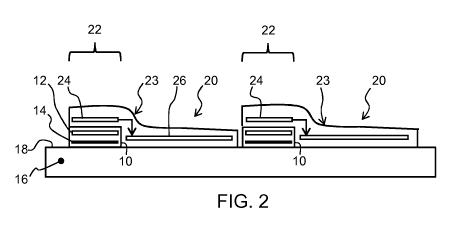
Figure 2 shows a cross section (in a horizontal plane) through a part of the
ships' hull 16 and part of the system including two of the first panels 10 and
two of the
second panels 20. The surface 18 of the hull is the surface to be protected
from fouling and
to this end the first panels 10 and the second panels 20 are mounted against
this surface 18.
As indicated hereinabove, this means that the surfaces 23 of the panels 20 now
effectively
have become the surface exposed to antifouling. Water between the system and
surface is
ignored for now as in this example the panels 20 are attached to the surface
in a
substantially watertight fashion.
The first panels 10 each have an inductive power emitter 10 of which in turn
each comprises at least one power emitter coil 12 the windings of which extend
in a plane
vertical to the plane of drawing. The power transmission lines of the
inductive power
emitters in panels 10 to which the power emitter coils 12 are connected are
not drawn in
the Figure but in this case would run vertical to the plane of drawing.
Each of the panels 20 comprises an inductive power receiver 20 of which
each one comprises a power receiver coil the windings of which also extend in
a plane
vertical to the plane of drawing. The power receiver coils are located in edge
regions 22 of
the panels 20 and the first and second panels are mounted to the surface such
that the edge
regions 22 of second parts 20 overlap with the second parts 10 so that power
emitter coils
12 overlap with power receiver coils 24. This may give a good inductive power
transfer
between the first and power receiver coils and therewith between power
transmitter and
receiver.
In this case counted from the surface of the ship, the panels 20 are
overlapping over the panels 10 in the edge regions. This may also be the other
way around.
The panels 20 each have one or more light sources arranged in a light source
arrangement 26 so arranged as to provide antifouling light at least to the
surfaces 23. The
wirelessly transmitted power by the panels 10 is used by the panels 20 to
power the light
sources in the arrangements 26.
CA 03113121 2021-03-17
WO 2020/058332 PCT/EP2019/075000
19
In the current example the ships' hull is made of steel in which Eddy
currents may occur at the locations of coils during power transfer. Such Eddy
currents may
reduce efficiency of power transfer. To reduce or prevent such loss of
efficiency, the
second panels 10 have a ferrite material in the form of a ferrite sheet 14
between the power
emitter coil and the metal of the hull 16 of the ship. The ferrite material
reduces or even
prevents Eddy currents in the metal of the ship's hull 16 thereby increasing
the efficiency
of energy transfer. High permittivity materials could also be used for this
purpose. It will
be clear that when Eddy currents do not significantly occur, such ferrite
material or other
solutions are not needed. For example when the hull is made of non-conducting
material
such as plastic or wood.
The power emitter coils may be formed on or within a printed circuit board
(PCB) which in turn may be part of the inductive power emitter and/or power
transmission
lines. Likewise, the power receiver coils may be formed on or within a PCB of
an
inductive power receiver. The light source arrangement may also be formed on a
PCB,
which may be separate to, or the same as, the PCB of the power receiver coils.
The PCBs
are not shown in the figures, to keep the shown structure simple. The PCBs are
thus also
parts of the respective panels.
There may be a single shared flexible PCB in a panel for example having the
coils and the light sources as well as other parts of the electronic power
provision circuit
within a panel. Such flexible panel is then capable to adapt to the contour of
the surface they
are mounted on. Instead, there may be separate PCBs in the panel and an
electrical
connection between them.
Electrical circuits in the form of PCBs are convenient, but need not be used
perse. Other ways of making the electrical circuits can be used as well.
Parts of the panel circuits may be made using PCB while other parts may be
made with different methods. For example, the light source arrangement may be
formed as
a wire grid structure instead of a PCB having distributed light sources. This
reduces the PCB
area since a PCB is needed only for the power receiver coils. In further
variants, the entire
panel circuits are devoid of PCB and made with other techniques.
The power emitter coils of the inductive power emitters 10 may for example
be supplied with a 100 kHz to 150 kHz AC supply (sinewave) during operation of
the
system. To compensate for a capacitive leakage current to the hull 16 at the
position of the
CA 03113121 2021-03-17
WO 2020/058332 PCT/EP2019/075000
power transmission lines, these (and therewith the inductive power emitter)
may further be
provided with a capacitor to implement a low pass filter. This is for example
of interest if
high efficiency switched amplifiers are used to generate the AC supply. In
such a case, the
low pass filter is used to filter out residual higher frequency harmonics of
the amplifiers.
5 An alternative is to use a resonant circuit to generate the AC
supply. For
example, each power transmission line (inductive power emitter) may comprise a
resonant
circuit, based on a capacitive resonant circuit, with a resonance in the range
60kHz to
90kHz.
Generally, the frequency of operation (resonant or driven) may be in the
10 range 50kHz to 1MHz, for example 50kHz to 200kHz, for example 60kHz to
90kHz.
Figure 3 shows exemplifying arrangements of panels and their overlap.
The example of Figure 2 has the panels 10 overlapping an associated panel
10 at one lateral edge. In Figure 3, the panels 20 overlap panels 10 at both
lateral edges,
and each panel 10 has pairs of power emitter coils, e.g. horizontally
neighboring 12a and
15 12b, arranged along its length (length is vertical in the plane of the
drawing). One coil of a
pair, e.g. 12a, is for powering a second panel 20 to one side and the other
coil of the pair,
e.g. 12b, is for powering a second panel 20 to the other side. In this way,
each second panel
20 is supplied by power from two sides and thus from two different first
panels. This
principle may be extended to more than two sides when a grid of first panels
is used
20 instead of a set of more or less parallel extending first panels 10.
This may make the
system more redundant against damage of first panels 10 and or of second
panels 20.
All power emitter coils of the first panels 10 can have the same phase,
which contributes to electric redundancy of the system. The light source
arrangements 26
can still function in their entirety if a power transmission line in the
inductive power
emitter of a first panel is broken. In that respect, the inductive power
emitters and the
power transmission lines may be designed to deliver electric power at an
increased level of
two times a normal level.
Thus, there may be one coil assembly (i.e. power emitter coil and power
receiver coil) per panel (Figure 2) or two coil assemblies per panel (Figure
3). There may
even be more than two with assemblies on yet further sides of panels (not
shown).
The first panel and the second panels of the antifouling system comprise
encapsulation material for protecting parts and especially electrical parts of
the system
CA 03113121 2021-03-17
WO 2020/058332 PCT/EP2019/075000
21
involved in powering of the system. That is, all parts of the system that are
normally
exposed to the water when the system is in use have such encapsulation. Thus,
in the
example described herein above, a panel includes such encapsulation which
encapsulates
its electrical circuits responsible for receiving power and driving of the
light sources. The
encapsulation in this case is for all of the electrical parts including for
example the coils,
power conduction lines and PCBs. An exception could possibly be a sensor
device in a
panel or at least those parts of the sensor device that need galvanic contact
with water to be
able to provide a sensory function. Preferably however in the system sensors
that operate
on a sensory principle that does not require galvanic electrical contact are
employed (e.g.
capacitive or other). The encapsulation prevents or at least reduces water
reaching these
electrical power provision parts and driving circuits of the system. The
encapsulation may
have the form of material in which all electrical components are embedded. The
material
may be called a water tight material having at least a reduced water
penetration
characteristic. The panel may thus be called a water tight panel. Suitable
materials for this
purpose will be described herein below but one type is based on silicone
polymers.
The panels 10 of the system also comprise encapsulation material to
encapsulate the inductive power emitter including coils, power transmission
lines and
PCB's or other. However, there may be a galvanic connector for connection to a
power
source that is to the outside of a panel 10. Such connector or connection is
then preferably
at a location of such panel 10 that is positioned on a surface part that is
not submerged in
water during use of the ship thus for example above the waterline.
With such encapsulated modular system there are no galvanic electrical
contacts for providing power from the strip to a panel or vice versa (if
needed) or between
panels. Hence while the encapsulation may reduce or prevent corrosion, power
can be
conveniently provided to the different watertight parts of the modular system.
At the same
time the systems modularity is preserved to provide an advantageous setup for
efficient
coverage of surface areas to be protected such as the ship's hull.
As shown in for example Figure 1, the antifouling system has multiple first
panels 10 and panels 20 for covering a surface of the ship. For example there
may be more
than 2, more than 5 more than 10 more than 20 or even more than 50 panels 20
coupled to
an inductive power emitter of a first panel 10. In a simplest arrangement to
cover a surface
there is only one first panel 10 and a plurality of second panels 20 each
associated with the
CA 03113121 2021-03-17
WO 2020/058332 PCT/EP2019/075000
22
single first panel 10 to be powered by that panel. However in the example of
Figure 1 there
are multiple first panels 10 and a plurality of second panels 20 is coupled to
each of these
multiple first panels 10.
With such a modular system application of the system to a surface may be
facilitated or more convenient in relation to a single element system. Also
irregular and or
non-flat shaped surfaces such as curved surfaces (as may happen with a ship's
hull) can be
more easily covered. The freedom in alignment of coils of a transformer
(alignment of
primary and power receiver coils) will be beneficial in this respect. It is
noted however that
such freedom is needed only during application of the system to the surface or
object as
once applied it is to be retained in a fixed position or configuration (apart
from situations
of repair). The number of second panels 20 per first panel 10 and/or number of
panels 10
and 29 per surface area may be chosen as desired based on the one hand on
shape, area and
dimensions of panels and on the other hand on the areas and dimensions of the
surface to
be covered. With the system a flexible design option for the antifouling
system can be
realized.
In the example shown, the first panels 10 and thus the inductive power
emitters 10 and the included power transmission lines extend in a
substantially vertical
orientation along the side of the ship. The second panels 20 are arranged
successively
along the length direction of such a first panel 10 and extend substantially
laterally with
respect to this length direction. However, any suitable arrangement of panels
is possible.
The first panels may be parallel to each other, but this need not be the case.
They may
make an angle of less than 90 degrees with the water line of the ship. They
may even be
parallel to the waterline of the ship. They do not need to be straight, but
may have one or
more curves or bends. This may be advantages for application to surfaces that
are not
inherently flat. In such case the panels may also have a shape adapted to
fulfill this purpose
of coverage of inherently non-flat surfaces. The panels 10 may for example
cover welding
seams and/or other surface irregularities of the ship's hull. In all cases it
may be
advantages to have a first panel extend to above the water line to allow a
contact to a
general power source such as the ships generators to be located in a non-
submerged area
when the ship is in use.
Figure 4 shows a cross section of an example of the structure of the second
panel 20 having a plurality of light sources 40 which in this example are side-
emitting UV-
CA 03113121 2021-03-17
WO 2020/058332 PCT/EP2019/075000
23
C LEDs, wherein the light is emitted primarily from a side of the LED, and
more or less
parallel to the surface 52. Other configurations may work too. The light
sources 40 are
encapsulated and in this case, although not needed per se, embedded in an
optical medium
or material 42 to guide at least part of the light 44 emitted from the light
sources 40 via
total internal reflection through the optical medium or material. The light is
guided at least
towards the surface 52 of the panels exposed to water but may also be guided
to other
surfaces or parts such as the surface opposing the surface 52. This medium or
material may
be and preferably is the same as the water tight encapsulation material
mentioned herein
before. Again suitable materials will be described herein below.
Optical structures 46 are provided to disrupt the total internal reflection
and
scatter light, and then guide the scattered light 48 out of the optical medium
42 towards a
target for the light, which is an area where a biofouling organism is present.
These optical
structures are not needed per se.
A biofouling organism on the surface 52 will directly receive the scattered
light 48 before it enters the water so that the light may exerts its
antifouling effect by
disrupting important biochemical growth mechanisms of the organisms as
described in the
art. Especially UV-C light has been found to be effective in this respect.
The optical medium is relatively thin so that the panel may be considered to
be a two-dimensional structure having a thickness of for example less than 3
cm or
preferably less than 2 cm or even less than 1 cm. The optical structures 46 to
scatter light
may be spread in one or more portions of the optical medium material, possibly
throughout
all of it, and the light output may be generally homogeneous or else
localized.
Internal scattering centers with different structural properties may be
combined to provide optical and well as structural characteristics, such as
resistance to
wear and/or impact. Suitable scatterers comprise opaque objects but largely
translucent
objects may be used as well, e.g. small air bubbles, glass and/or silica; a
requirement is
merely that a change in refractive index occurs for the wavelength(s) used.
The principle of light guiding and spreading light over a surface is well-
known and widely applied in various fields. Here, the principle is applied to
UV light for
the purpose of antifouling.
To maintain the conditions for total internal reflection, the index of
refraction of the light guiding material should be higher than that of the
surrounding
CA 03113121 2021-03-17
WO 2020/058332 PCT/EP2019/075000
24
medium. However, the use of (partly) reflecting coatings on the light guide
and/or the use
of the reflective properties of the protected surface, e.g. the hull of a
ship, itself can also be
used to establish the conditions for guiding the light through the optical
medium.
In the example above, the panels form a new surface over the surface to be
protected (the surface of the object which in this case is the outer surface
of the hull of a
ship), and light is directed outwardly from the surface to be protected.
However, an
alternative is for the panel to be spaced over the surface to be protected and
to direct light
back towards the surface to be protected. A combination of the two is also
possible in that
the panels may direct their emitted light to its opposing surfaces one of
which will face the
water and one of which will face the hull surface.
A small air gap may then be introduced between the light source
arrangement of the panel and the surface to be protected. UV light may travel
better, with
less absorption, in air than in an optical medium, even when this optical
medium is
designed as a light guiding material.
As most materials have a (very) limited transmittance for UV light, care has
to be taken in the design of the optical medium. As a result, a relatively
fine pitch of low
power LEDs can be chosen, to minimize the distance light has to travel through
the optical
medium.
In one example, the optical medium 42 comprises a silicone based material,
and one which is designed to have good UV-C transparency.
A solid encapsulation may be used in which case parts of the panel are
embedded in the encapsulation material, as shown in Figure 4. However, a
hollow
structure may instead be used, such as a silicone mat with spacers that keep
it a small
distance away from the protected surface. This creates air channels, through
which the UV
.. light can propagate with higher efficiency. Use of gas filled channels
provided by such
structures allows distributing the UV light over significant distances in an
optical medium
of material that would otherwise absorb the UV light too strongly to be useful
for
antifouling. Similarly, separate pockets may be formed.
Figure 5 shows an electrical configuration of an antifouling system, for
example the one of the system of Figure 1.
The system includes a power source for delivering power to the inductive
power emitter. The power source comprises an AC driver 60, a tuning coil 62
and a tuning
CA 03113121 2021-03-17
WO 2020/058332 PCT/EP2019/075000
capacitor 64. The power source connects to the inductive power emitter 10 of
the system by
a cable 66. In particular the cable leads connect to the power feed line 70
and the power
return line 72 of the power transmission line. This connection between the
power transmitters
and the power source can now be made galvanic and above the waterline of a
ship where
5 such galvanic connections are less prone to corrosion in watery
conditions. In the
arrangement shown, the inductive power emitter 10 comprises a set of power
emitter coils
12 (5 are shown) arranged physically in a line along the power transmission
line, but
electrically connected in parallel.
The panel (only one of which is shown for clarity) includes the power receiver
10 coil 24, aligned with and therefore magnetically coupled to one of (the
top shown one) the
power emitter coils 12. The coils are shown next to each other in the drawing
and although
this may in practice be a real situation, preferably the coils are designed
and arranged such
that they are on top of each other as described herein before.
For long power transmission lines for driving many second panels, such as
15 e.g. more than 10, the power transmission line is preferably at least
partly balanced and more
preferably fully balanced. A balanced transmission line may be a transmission
line consisting
of two conductors of the same type, each of which have equal impedances along
their lengths
and equal impedances to ground and to other circuits. The power transmission
line then
behaves as a balanced transmission line and can then be driven with a balanced
driver such
20 as an H-bridge. This has advantages for electromagnetic compatibility
(EMC) and for the
driver, for example because both PCB leads, i.e both the power feed line lead
and power
return line lead of the power transmission line, can see the same impedance
(e.g. same
capacitance) to the ship's hull and to the water. In a balanced situation the
EMC stray fields,
which deteriorate the emission behavior at the driving frequency, will balance
out. This
25 improves antenna efficiency.
The balanced power transmission line can be made in the form of a twin lead
with two conductor strips held at a precise constant mutual distance along the
transmission
line and with an insulator in between the conductor strips. This allows use of
a single metal
layer PCB and may provide a thin solution for the system. Alternatively, or
additionally, the
power transmission line can be a twin lead including two metal conductors on
top of each
other with an insulator layer in between. Again the distance between them is
kept at a
constant value along the conductors lengths. In such case the power feed line
may be on top
CA 03113121 2021-03-17
WO 2020/058332 PCT/EP2019/075000
26
of the power return line of a power transmission line or vice versa with
reference to the
systems' surface attached to the object surface when in use.
A two layer PCB design may also be used to enable cross overs in conductors
to be formed for example close to the coils as there will be windings
connected to the power
transmission line.
Figure 6 is shows an arrangement in which the power feed line 70 is down
one side of the power emitter coils and the power return line 72 is down an
opposite side of
the power emitter coils. Less crossovers may be needed for connections.
However, the
magnetic field in the coils is now dependent on the current through the power
power power
feed lines as the current through a power feed line and a power return line
both generate a
magnetic field which fields add up at the inner coil areas, i.e. they add to
the magnetic flux
of the coils. As current passes along the power feed line, current is tapped
off by each coil
in turn (thus coil Cl tapps of before coil C2) and, as a result, the total
current flowing thus
depends on the position along the power feed line. For example, at one
location, the current
is NIcom where Icom is the current drawn by each power emitter coil, and there
are N coils
still to be supplied with current. Past the next coil, the current is (N-1)
Icon,. Thus, the
current generating a magnetic field in a particular coil is a function of
position of the coil.
As a result, the power transmission within a particular coil is a function of
position of that
particular coil along the inductive power emitter (or panel it is part of).
This means the
different power receiver coils driven by different power emitter coils may be
driven to
different voltages or currents. In some cases this is an advantage but in
others it may be a
disadvantage.
Figure 7 shows a first approach to address this disadvantage. The inductive
power emitter 10 again comprises a plurality of power emitter coils 12 (C1 and
C2 are
shown) electrically in parallel positioned physically series along the length
of the power
transmission line. The power feed line 70 extends from one end of the feeding
line to the
plurality of power emitter coils and the power return line 72 extends from the
plurality of
power emitter coils to the one end of the feeding line. The power feed line
and the power
return line in this case are side by side and in this case at one side of a
power emitter coil. In
this case even to the same side of multiple power emitter coils, but this is
not necessary per
se. In this way, the magnetic fields caused by the power feed line and power
return line
(which are of different strengths along their length as a result of the
tapping off of current
CA 03113121 2021-03-17
WO 2020/058332 PCT/EP2019/075000
27
between coils) are substantially cancelled at the power emitter coil location.
Consequently a
more uniform magnetic field strength is achieved within the power emitter
coils.
The arrangement may for example be driven with a voltage controlled driver
to ensure the voltage does not exceed safety levels.
Figure 8 shows a second approach to address the non-uniform power
transmission of Figure 6. The inductive power emitter 10 comprises a single
coil extending
along the length of the transmitter or panel. It is as if the coil also
performs the function of
feeding line. The single coil is then for magnetic coupling to the power
receiver coils of the
plurality of inductive power receiver panels to be associated or driven by
this inductive
power emitter. Thus, a single power emitter coil, formed of a power feed line
70 and power
return line 72 with a connecting bridge 74 at the end of the feeding line is
used to
magnetically couple to a set of power receiver coils. In this way, the
magnetic field coupling
to each power receiver coil is the same or close to the same.
The use of a single coil relaxes the vertical and/or angular accuracy with
which the power receiver coils need to be aligned with the power emitter
coils. The
arrangement may for example be driven with a voltage current controlled driver
or current
controlled driver. The use of one power emitter coil only means the voltage is
more easily
controlled so that current driving is also an option. The power emitter coil
again may have
multiple windings such as 1 to 5.
Figure 9 shows a third approach to address the non-uniform driving
disadvantage indicated herein before in relation to the example of Fig. 6. In
this third
approach the inductive power emitter comprises a set of conductive elements in
the form of
power transmission lines 10a, 10b. Each feeding line is associated with a
respective plurality
of inductive power receiver panels which each extend laterally from a
respective position
along the feeding line. Feeding line 10a is associated with (and provides
power to) panel 20a
and also other panels forming other rows (not shown). Feeding line 10b is
associated with
(and provides power to) panel 20b and also other panels forming other rows
(not shown).
Each feeding line 10a, 10b comprises a power feed line 70a, 70b and a power
return line 72a, 72b. The power power feed lines and power return lines each
extend from a
first end of the feeding line (the top in Figure 9) to a second end of the
feeding line (the
bottom in Figure 9). The power feed line and the power return line of any
given power
CA 03113121 2021-03-17
WO 2020/058332 PCT/EP2019/075000
28
transmission line form parts of a conductive element capable of transferring
power. After
all, their neighboring parts generate magnetic fields between them that may
add up.
Thus, in this implementation the individual feeding lines do not have coils.
Instead, they define one half (e.g. the feed part) of one power emitter coil
and one half (e.g.
the return part) of another power emitter coil. There is again one quasi power
emitter coil
(no actual windings are formed) which extends over the full length of the pair
of feeding
lines.
Connecting members 76 are provided between the second ends of adjacent
feeding lines, to connect the power feed line e.g. 70a of one feeding line 10a
with the power
return line e.g. 72b of an adjacent feeding line 10b to one side (the right in
Figure 9) and to
connect the power return line 72a of said one feeding line 10a with the power
feed line an
adjacent feeding line to the other side (the left in Figure 9, not shown). The
connecting
members are away from the panels. The leakage inductance caused by the
connecting
members 76 can be tuned with a capacitor at the first (top) end of the feeding
line to make
the overall arrangement function as a resistive load, thereby improving
efficiency by
cancelling blind currents.
A first current Ii flows down power feed line 70a and back via power return
line 72b. The power receiver coil 24 overlaps the pair of adjacent feed and
power return
lines at the location where the magnetic field of these power power feed lines
add up. Thus,
the current flows in large loops, but the magnetic coupling to the power
receiver coils 24 is
by means of the local oppositely flowing currents.
To ensure the local currents (e.g. TO and II) flow in opposite directions to
make the magnetic fields of power power feed lines add up at the desired
locations, adjacent
large loops are driven out of phase with each other.
This third option arrangement may be easier to mount to a surface.
In the examples above, the second panels 20 overlap the first panel 10 in
order
to have power receiver coils overlap power emitter coils. This provides
galvanic isolation
between the power supply and the structure which is exposed to the water. The
panel also
protects the underlying feeding line. Instead, or in addition the first panels
may be provided
over the second panels. A separate electrical isolation may be provided (e.g.
at the top of
the feeding lines). The surface of the strips may then be susceptible to
biofouling, so it
should then be ensured that light reaches the surface of the feeding lines,
either by
CA 03113121 2021-03-17
WO 2020/058332 PCT/EP2019/075000
29
transmission through the feeding lines or by reflection or waveguide
transmission within the
panels or by adding a light sources to the first parts.
Thus in the above examples, the inductive power emitter and the panel are
both for mounting over the surface, but in either order.
Alternatively, only the panels are mounted over the surface. The strips are
still applied to the object such that power emitter coils align with power
receiver coils, but
not to the same surface. For example, the strips are applied to the inside of
the ship's hull
and power is then transferred through the ship's hull. A wooden or plastic
hull could work
in that way. Alternatively, the hull could have holes for harboring the power
emitter coils.
As mentioned, some of the examples above makes use of a ferrite sheet 14
below the windings to reduce Eddy currents. An alternative shown in Figure 10
is to provide
the inductive power emitter 10 and inductive power receiver 20 over a paint
material 100 on
the surface. The paint material includes ferromagnetic or other high
permeability particles
such that it has a relative magnetic permeability greater than 20, for example
greater than
100 or even greater than 200. The additional layer for preventing the eddy
currents may also
be omitted. For example when a ship's hull is less prone to providing such
currents. This
could be in case of wooden or plastic type hulls.
A high permeability paint can function as a replacement for a ferrite layer.
It
has good insulation properties but conducts magnetic field. Thus, it functions
to shape the
magnetic field but prevent induced currents in the underlying conducting
layer, such as a
ship's hull.
For the application of the invention to a biofouling prevention system, a
typical secondary side current is 0.1A and a typical desired secondary side
voltage is
around 40V. For safety, a maximum voltage of 50V rms (by way of example only)
may be
considered. The system is designed or operate below the maximum voltage,
taking into
accout all the characteristics of the inductive coupling and the spreading of
currents. For a
given operating voltage, the required current depends on the required power. A
higher
voltage enables a lower current and vice versa.
The feeding lines for example make use of a PCB with thickness of less than
1 mm, for example 0.5 mm, created a molded structure thickness of around 3 mm.
The panels for example have a PCB thickness of 0.8 mm, and the total
thickness with the silicone of below 5 mm, for example in the range 2 mm to 4
mm.
CA 03113121 2021-03-17
WO 2020/058332 PCT/EP2019/075000
A panel may have many shapes such as triangular or rectangular. They may
have an area of 0.5 m2 or larger. Preferably they have an area of 2.5 m2 or
larger. The sides
of such panels may be of dimensions (length and width) larger than 0.1 or 0.2
meter,
preferably larger than 0.5 meter. Not all sides of a panel, or of different
panels in case there
5 are more in a system, need to have the same dimensions. The panels for
example have a
length (along the horizontal row direction) in the range 1 m to 5 m and a
height (along the
vertical column direction) in the range 50 cm to 150 cm. For example a small
panel
dimension may be 600 mm x 1200 mm and a large panel dimension may be 1 m x 4
m. An
example area to be covered, e.g. one side of a ship hull, may be of the order
of 100 m
10 length by 10 m height. But this may all depend on the size of the
surface to be covered and
thus the size of the object.
The shapes and sizes (area) or dimensions (length, width) of the strip and
panels may be any as long as suitable for use in an antifouling system to be
able to protect
ore even cover the surface. They shapes and sizes may be chosen according to
size and shape
15 of the surface they need to be applied to. Since the surface preferably
is one of an object such
as a vessel, and ship, etc., such surfaces are in general quite large, i.e.
larger or much larger
than 1 m2
The first panel 10 may have any shape, but preferably is elongate and more
preferably is also rectangular. It preferably has a length larger than 0.2
meter, or larger than
20 0.5 meter. Even more preferable is a length longer than 1 meter or
longer than 5 meters. The
width of a first panel may be any dimension as long as its electrical
components such as e.g.
coils and/or power transmission lines can be housed. They could have a width
wider than
any one of the following values: 0.1 meter, 0.2 meter, 0.3 meter, 0.4 0.5
meter or larger.
The antifouling implementation is of interest for objects to be at least
partly
25 submerged in water, where water means any type of water known to host
biofouling
organisms such as river, lake or sea water. Examples of marine objects include
ships and
other vessels, marine stations, sea-based oil or gas installations, buoyancy
devices, support
structures for wind turbines at sea, structures for harvesting wave/tidal
energy, sea chests,
underwater tools, etc. and parts of all of these. For biofouling prevention,
the system may
30 be applied to lock doors, silo tanks in the food industry, and drinking
water vessels.
The antifouling use of the invention can be applied to a wide variety of
fields. Almost any object coming into contact with natural water, will over
time be subject
CA 03113121 2021-03-17
WO 2020/058332 PCT/EP2019/075000
31
to biofouling. This can hinder e.g. water inlets of desalination plants, block
pipes of
pumping stations, or even cover the walls and bottom of an outdoor pool. All
of these
applications would benefit from the presently provided method, lighting
modules and/or
system, i.e. an effective thin additional surface layer, which prevents
biofouling on the
.. entire surface area.
In preferred examples, the light sources are UV LEDs as explained above. A
grid of UV LEDs may be encapsulated in a liquid-tight encapsulation, of which
silicone is
only one example. The UV LEDs may be electrically connected in a series and/or
parallel
arrangement. The UV LEDs are for example packaged surface mount LEDs, in which
case
they already may include an optical element to distribute the light emitted
from the LED
package across a wide emission angle. In other embodiments, the UV LEDs may be
LED
dies, typically not comprising optical elements but being significantly
thinner than
packaged LEDs. As an example, LED dies could be picked and placed onto a
surface of
the optical medium
The silicone material that can be used as encapsulation material and/or
optical material can be selected to provide optical transmission for UV light
with little loss
compared to other materials. This is in particular the case for shorter
wavelength light, e.g.
UV light with wavelengths below 300 nm. A particularly efficient group of
silicone
materials is, or at least comprises, so-called methyl silicones, according to
the general
chemical formula CH3[Si(CH3)20].Si(CH3)3, with "n" indicating any suitable
integral.
Silicone materials are also flexible and resilient so that they are robust,
durable and capable of withstanding compression such as due to bumps,
collisions etc. of
objects against the surface, e.g. bumping of a ship against a quay.
Furthermore,
deformation due to temperature fluctuation, pounding by waves, flexion of the
ship over
swell etc. may be accommodated.
The encapsulation may have multiple materials that may be layered as
known in the contemporary art in this new light based antifouling systems
field.
At least part of light emitted by the one or more light sources may be spread
in a direction having a component substantially parallel to the surface to be
protected. This
facilitates distributing the light over significant distances along the
protected surface, or the
application surface of the foil, which assists in obtaining a suitable
intensity distribution of
the antifouling light.
CA 03113121 2021-03-17
WO 2020/058332 PCT/EP2019/075000
32
A wavelength conversion material may be comprised in the optical medium
and at least part of the antifouling light may be generated by photo-exciting
the wavelength
conversion material with light having a first wavelength causing the
wavelength
conversion material to emit the antifouling light at another wavelength. The
wavelength
conversion material may be provided as an up-conversion phosphor, quantum
dots,
nonlinear media such as one or more photonic crystal fibers etc. Since
absorption and/or
scattering losses in the optical medium for light of different, mostly longer,
wavelengths
than UV light tend to be less pronounced in the optical media, it may be more
energy-
efficient to generate non-UV light and transmit that through the optical
medium and to
generate UV antifouling light at or near the desired location of use thereof
(i.e. emission
form the surface into the liquid environment).
One example described above makes use of side-emitting LEDs and optical
scattering sites. However, light spreading arrangements may be used to create
the sideways
light. For example, a cone may be arranged in the optical medium and
positioned opposite
the light source, where the opposing cone has a surface area with a 45 angle
perpendicular
to the protected surface for reflecting light emitted by the light source
perpendicular to said
surface in a direction substantially parallel to said surface.
The LEDs may be DC driven. However, a pair of back to back parallel
LEDs may be driven by an AC drive signal.
As mentioned above the LEDs are preferably mounted on a PCB, and PCB
tracks (on the PCB surface or internally within layers of the PCB) form the
receiver coil.
However, the LED grid may instead be formed by connecting LEDs to a connection
nodes
of a freestanding wire structure by soldering, gluing or any other known
electrical
connection technique. This may be combined with a power receiver coil on a
smaller PCB.
Although UV light is the preferred solution, other wavelengths are
envisaged as well. Non-UV light (visible light) is also effective against
biofouling. Typical
micro- organisms are less sensitive to non-UV light than to UV light, but a
much higher
dose can be generated in the visible spectrum per unit input power to the
light sources.
UV LEDs are an ideal source for thin light emitting surfaces. However, UV
sources other than LEDs can also be used, such as low pressure mercury vapor
lamps. The
form factor of these light sources are quite different; mainly the source is
much bigger.
This results in different optical designs, to distribute all the light from a
single source over
CA 03113121 2021-03-17
WO 2020/058332 PCT/EP2019/075000
33
a large area. Further, a significant contribution of light in desired
wavelengths and/or
wavelength combinations may be produced. Instead of using a thin layer that
emits UV
light outward in a direction away from the protected surface in order to avoid
bio-fouling,
biofouling could potentially also be removed by applying UV light from the
outside in the
direction of the protected surface, as explained above. The panel may instead
emit
antifouling light both in directions towards and away from the surface to be
protected.
The antifouling system exemplified are based on providing antifouling light
used for protecting a surface against biofouling while the surface is
submerged in water.
While this is a preferred application area where the system may have its
profound
advantages, the use of the system is not necessarily limited to such
circumstances as
submergence in water as biofouling may also occur on surfaces exposed to the
atmospheric
environment.
Variations to the disclosed embodiments can be understood and effected by
those skilled in the art in practicing the claimed invention, from a study of
the drawings,
the disclosure and the appended claims. In the claims, the word "comprising"
does not
exclude other elements or steps, and the indefinite article "a" or "an" does
not exclude a
plurality. The mere fact that certain measures are recited in mutually
different dependent
claims does not indicate that a combination of these measures cannot be used
to advantage.
If the term "adapted to" is used in the claims or description, it is noted the
term "adapted
to" is intended to be equivalent to the term "configured to". Any reference
signs in the
claims should not be construed as limiting the scope.