Note: Descriptions are shown in the official language in which they were submitted.
CA 03115263 2021-03-31
WO 2020/077100
PCT/US2019/055655
DEVICE WITH DISPOSABLE ELEMENT
CROSS REFERENCE TO RELATED APPLICATIONS
[0001] This application claims the benefit of U.S. Provisional Application No.
62/744,513,
filed October 11, 2018, and U.S. Provisional Application No. 62/804,095, filed
February 11,
2019, the contents of each of which are herein incorporated by reference in
their entireties
and for all purposes.
FIELD
[0002] The present disclosure provides apparatus and methods for a device for
detecting
tissue damage through measurement of Sub-Epidermal Moisture (SEM). The present
disclosure further provides apparatus and methods for a device for detecting
tissue damage
through measurement of SEM, where the device includes a printed circuit board
(PCB)
assembled into a molded frame.
BACKGROUND
[0003] A printed circuit board (PCB) is employed in medical devices as a flat
base that
physically supports and electronically connects electronic components and
conductors. PCBs
may be single-sided, double-sided, and multilayered. PCBs are currently
retained in device
frames by either adhesive or provision of a lip in the frame that captures the
edge of the PCB.
SUMMARY
[0004] In an aspect, the present disclosure provides for, and includes, a
detachable element
for use with a reusable component having a retention groove and an alignment
guide and a
planar contact surface parallel to the retention groove, the detachable
element comprising: a
body comprising a retention feature configured to engage the retention groove,
and an
electrical contactor coupled to the body, where the contactor comprises a
cantilever element
that is configured to touch the planar contact surface when the retention
feature is engaged
with the retention groove, where the cantilever element is configured to slide
along the
contact surface as the detachable element is brought together with the
reusable component.
[0005] In an aspect, the present disclosure provides for, and includes, a
connector
comprising: a reusable component comprising a retention groove and an
electrical contact
surface that is parallel to the retention groove; and a detachable element
comprising a body
1
CA 03115263 2021-03-31
WO 2020/077100
PCT/US2019/055655
with a retention feature configured to engage the retention groove and an
electrical contactor
coupled to the body, where the contactor comprises a compliant element that is
configured to
touch the contact surface of the reusable element when the retention feature
of the detachable
element is engaged with the retention groove of the reusable component and to
slide along
the contact surface as the detachable element is brought together with the
reusable
component.
[0006] In an aspect, the present disclosure provides for, and includes, a
detachable element
comprising: a body comprising a hole and a retention pocket, where the
retention pocket
comprises a reference surface; and a printed circuit board assembly (PCBA)
comprising a
printed circuit board (PCB) having an outer edge and a contactor coupled to
the PCB, where
a portion of the contactor extends beyond the outer edge of the PCB, where the
portion of the
contactor that extends beyond the outer edge of the PCB is in contact with the
reference
surface. In an aspect, an external surface of a PCB is flush with a surface of
a frame without
a protruding lip or the use of adhesive.
[0007] In an aspect, the present disclosure provides for, and includes, a
detachable element
comprising: a body comprising upper and lower sections joined by a flexible
arm, where the
upper section comprises an opening and the lower section is attached on its
underside to a
compressible spring; and a printed film having tabbed and non-tabbed areas,
where the
tabbed area comprises a sensor comprising two electrodes on one first face,
and where the
tabbed area is inserted between the upper and lower sections so that the
sensor is aligned with
the opening.
BRIEF DESCRIPTION OF THE DRAWINGS
[0008] Aspects of the disclosure are herein described, by way of example only,
with
reference to the accompanying drawings. With specific reference now to the
drawings in
detail, it is stressed that the particulars shown are by way of example and
are for purposes of
illustrative discussion of aspects of the disclosure. In this regard, the
description and the
drawings, considered alone and together, make apparent to those skilled in the
art how
aspects of the disclosure may be practiced.
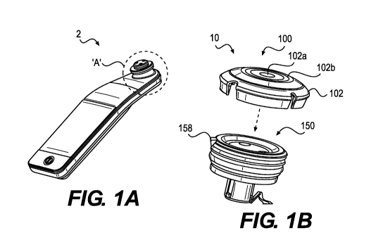
[0009] Fig. lA depicts a medical scanner, in accordance with the present
disclosure.
[0010] Fig. 1B depicts a connector comprising a reusable component, which is
part of the
medical scanner of Fig. lA in the region "A," and a detachable element, in
accordance with
the present disclosure.
2
CA 03115263 2021-03-31
WO 2020/077100
PCT/US2019/055655
[0011] Fig. 2 is a perspective view of the underside of the detachable element
of Fig. 1B, in
accordance with the present disclosure.
[0012] Fig. 3 is a perspective view of the top surface of the reusable
component, in
accordance with the present disclosure.
.. [0013] Fig. 4 is a side view of the reusable component, in accordance with
the present
disclosure.
[0014] Fig. 5 is a side view of the detachable element mated with the reusable
component, in
accordance with the present disclosure.
[0015] Fig. 6 is a cross-section of the side view of Fig. 5, in accordance
with the present
disclosure.
[0016] Fig. 7A is another perspective view of the underside of the detachable
element of Fig.
1B, in accordance with the present disclosure.
[0017] Fig. 7B is a partially exploded view of the detachable element of Fig.
7A, in
accordance with the present disclosure.
[0018] Fig. 8 is an enlarged cross-section of the region marked "B" in Fig.
7A, in accordance
with the present disclosure.
[0019] Fig. 9 is a second cross-section showing the configuration of the
region "B" after a
heat staking operation has been completed, in accordance with the present
disclosure.
[0020] Fig. 10 is an exploded view of an assembly comprising a frame, a PCB,
and a retainer.
[0021] Fig. 11A is a cross-section of a body, a PCB, and a retainer.
[0022] Fig. 11B depicts the items of Fig. 11A after assembly.
[0023] Fig. 12 depicts dimensions of an example sensor in accordance with the
present
disclosure.
[0024] Fig. 13A depicts an exploded view of an assembly comprising a flexible
frame with
one end of a printed film inserted between upper and lower sections of the
frame and the
other end of the printed film wrapped around the underside of a compressible
spring attached
to the bottom of the frame, in accordance with the present disclosure.
[0025] Fig. 13B depicts a top view of one face of an unfolded, printed film,
in accordance
with the present disclosure.
3
CA 03115263 2021-03-31
WO 2020/077100
PCT/US2019/055655
DETAILED DESCRIPTION
[0026] This description is not intended to be a detailed catalog of all the
different ways in
which the disclosure may be implemented, or all the features that may be added
to the instant
disclosure. For example, features illustrated with respect to one embodiment
may be
incorporated into other embodiments, and features illustrated with respect to
a particular
embodiment may be deleted from that embodiment. Thus, the disclosure
contemplates that,
in some embodiments of the disclosure, any feature or combination of features
set forth
herein can be excluded or omitted. In addition, numerous variations and
additions to the
various embodiments suggested herein will be apparent to those skilled in the
art in light of
the instant disclosure, which do not depart from the instant disclosure. In
other instances,
well-known structures, interfaces, and processes have not been shown in detail
in order not to
unnecessarily obscure the invention. It is intended that no part of this
specification be
construed to effect a disavowal of any part of the full scope of the
invention. Hence, the
following descriptions are intended to illustrate some particular embodiments
of the
disclosure, and not to exhaustively specify all permutations, combinations,
and variations
thereof.
[0027] Unless otherwise defined, all technical and scientific terms used
herein have the same
meaning as commonly understood by one of ordinary skill in the art to which
this disclosure
belongs. The terminology used in the description of the disclosure herein is
for the purpose
of describing particular aspects or embodiments only and is not intended to be
limiting of the
disclosure.
[0028] All publications, patent applications, patents, and other references
cited herein are
incorporated by reference in their entireties for the teachings relevant to
the sentence and/or
paragraph in which the reference is presented. References to techniques
employed herein are
intended to refer to the techniques as commonly understood in the art,
including variations on
those techniques or substitutions of equivalent techniques that would be
apparent to one of
skill in the art.
[0029] U.S. Patent Application Serial No. 14/827,375 ("the '375 application")
discloses an
apparatus that measures the sub-epidermal capacitance using a bipolar sensor,
where the
sub-epidermal capacitance corresponds to the moisture content of the target
region of skin of
a patient. The '375 application also discloses an array of these bipolar
sensors of various
sizes.
4
CA 03115263 2021-03-31
WO 2020/077100
PCT/US2019/055655
[0030] U.S. Patent Application Serial No. 15/134,110 discloses an apparatus
for measuring
sub-epidermal moisture (SEM), where the device emits and receives an RF signal
at a
frequency of 32 kHz through a single coaxial sensor and generates a
bioimpedance signal,
then converts a biocapacitance signal to a SEM value.
[0031] U.S. Patent Application Serial No. 13/942,649 discloses a compact
perfusion scanner
and method of characterizing tissue heath status incorporating optical sensors
to monitor
tissue blood perfusion measurements and oximetry.
[0032] U.S. Patent Application Serial Nos. 14/827,375, 15/134,110, and
13/942,649 are
incorporated herein by reference in their entireties.
[0033] Unless the context indicates otherwise, it is specifically intended
that the various
features of the disclosure described herein can be used in any combination.
Moreover, the
present disclosure also contemplates that in some embodiments of the
disclosure, any feature
or combination of features set forth herein can be excluded or omitted.
[0034] The methods disclosed herein include and comprise one or more steps or
actions for
achieving the described method. The method steps and/or actions may be
interchanged with
one another without departing from the scope of the present disclosure. In
other words, unless
a specific order of steps or actions is required for proper operation of the
embodiment, the
order and/or use of specific steps and/or actions may be modified without
departing from the
scope of the present disclosure.
[0035] As used in the description of the disclosure and the appended claims,
the singular
forms "a," "an," and "the" are intended to include the plural forms as well,
unless the context
clearly indicates otherwise.
[0036] As used herein, "and/or" refers to and encompasses any and all possible
combinations
of one or more of the associated listed items, as well as the lack of
combinations when
interpreted in the alternative ("or").
[0037] The terms "about" and "approximately" as used herein when referring to
a measurable
value such as a length, a frequency, or a SEM value and the like, is meant to
encompass
variations of 20%, 10%, 5%, 1%, 0.5%, or even 0.1% of the specified
amount.
[0038] As used herein, phrases such as "between X and Y" and "between about X
and Y"
.. should be interpreted to include X and Y. As used herein, phrases such as
"between about X
and Y" mean "between about X and about Y" and phrases such as "from about X to
Y" mean
"from about X to about Y."
5
CA 03115263 2021-03-31
WO 2020/077100
PCT/US2019/055655
[0039] As used herein, the term "sub-epidermal moisture" or "SEM" refers to
the increase in
tissue fluid and local edema caused by vascular leakiness and other changes
that modify the
underlying structure of the damaged tissue in the presence of continued
pressure on tissue,
apoptosis, necrosis, and the inflammatory process.
[0040] As used herein, the term "biocapacitance" refers to the physical
property that reflects
the relative dielectric permittivity of the tissue, i.e. how much resistance
to electrical fields is
encountered in tissues.
[0041] As used herein, a "patient" may be a human or animal subject.
[0042] As used herein, the term "parallel" describes configurations where best-
fit lines or
planes of two objects have an approximately constant separation over a
distance meaningful
to the application. In certain embodiments, these best-fit lines or planes may
have an
included angle of 1 degree, 5 degrees, or 10 degrees.
[0043] As used herein, the term "planar" describes configurations where the
actual surface of
an object varies from a best-fit ideal plane by a distance that is not
significant in the function
of the object. In certain embodiments, the distance between the actual surface
and the ideal
plane may be 0.254 mm (0.010 inches), 1.27 mm (0.050 inches), or 2.54 mm
(0.100 inches).
[0044] As used herein, the term "diameter" refers to the length of a straight
line segment that
passes through the center of a circle and whose endpoints lie on the circle.
The diameter is
equal to twice the radius of the circle.
[0045] As used herein, the term "toroid" refers to a circular surface of
revolution with a hole
or an opening in its center. As used herein, the term "concentric" refers to
two or more
objects having the same center or axis.
[0046] As used herein, the term "printed film" refers to a segment of a
polymeric film upon
which conductive elements have been printed.
[0047] As used herein, the term "pogo pin" refers to a spring-loaded
electrical connector
mechanism.
[0048] Fig. lA depicts a medical scanner 2, in accordance with the present
disclosure. In an
aspect, medical scanner 2 is an SEM scanner. In an aspect, medical scanner 2
is an SEM
scanner that measures biocapacitance. In an aspect, the nose of the device,
indicated by the
dashed line circle 'A,' is pressed against the skin of a patient to make an
SEM measurement.
In an aspect, the nose of the device, indicated by the dashed line circle 'A,'
is pressed against
the skin of a patient to make a biocapacitance measurement.
6
CA 03115263 2021-03-31
WO 2020/077100
PCT/US2019/055655
[0049] Fig. 1B depicts a connector 10 comprising a reusable component 150,
which is part of
the medical scanner of Fig. lA in the region 'A,' and a detachable element
100, in
accordance with the present disclosure. In an aspect, detachable element 100
comprises a
body 102 and a sensor formed from a center electrode 102a and a toroidal
electrode 102b,
where center electrode 102a and toroidal electrode 102b are concentric with
respect to one
another. Center electrode 102a has an outer-facing surface (visible in Fig.
1B) and an inner-
facing surface (not visible in Fig. 1B). Similarly, toroidal electrode 102b
has an outer-facing
surface (visible in Fig. 1B) and an inner-facing surface (not visible in Fig.
1B).
[0050] In an aspect, detachable element 100 comprises a sensor formed from a
plurality of
electrodes such as up to two electrodes, up to three electrodes, up to four
electrodes, up to
five electrodes, up to six electrodes, up to seven electrodes, up to eight
electrodes, up to nine
electrodes, up to ten electrodes, up to eleven electrodes, or up to twelve
electrodes. In an
aspect, detachable element 100 comprises a plurality of sensors formed from a
plurality of
electrodes, where each sensor is formed from up to twelve electrodes, such as
up to two
electrodes, up to three electrodes, up to four electrodes, up to five
electrodes, up to six
electrodes, up to seven electrodes, up to eight electrodes, up to nine
electrodes, up to ten
electrodes, or up to eleven electrodes. In an aspect, a sensor is formed from
an annular ring
disposed around an inner circular electrode. In an aspect, a sensor is formed
from two
parallel bar electrodes. In an aspect, a sensor is formed from electrodes in
the form of
interdigitating fingers. In an aspect, detachable element 100 comprises a body
102 and a
plurality of sensors selected from the group consisting of a plurality of
bioimpedance sensors,
a plurality of pressure sensors, a plurality of light sensors, a plurality of
temperature sensors,
a plurality of pH sensors, a plurality of perspiration sensors, a plurality of
ultrasonic sensors,
a plurality of bone growth stimulator sensors, and a plurality of a
combination of these
sensors. In an aspect, detachable element 100 comprises a body 102 and a
plurality of light
sensors. In an aspect, detachable element 100 further comprises one or more
light emitting
sources comprising dual emitters configured for emitting 660 nm and 880 nm
light. In an
aspect, reusable component 150 comprises an alignment guide 158, the function
of which is
described in greater detail with reference to Fig. 5. In this example,
detachable element 100
is mated to a reusable component by a linear movement, as indicated by the
dashed line. In
an aspect, the mating motion comprises a rotation perpendicular to the dashed
line or twists
about the dashed line. In an aspect, detachable element 100 comprises an
insulating cover
layer on top of its electrodes, forming a barrier between the electrodes and
the patient's skin
while measurements are being taken.
7
CA 03115263 2021-03-31
WO 2020/077100
PCT/US2019/055655
10051] In an aspect, a sensor formed from an annular ring disposed around an
inner circular
electrode as depicted in Fig. 12. In an aspect, an inner circular electrode is
defined by a
diameter Dl. In an aspect, D1 is about 4.318 mm (0.17 inches). In an aspect,
the annular
ring is defined by an inner diameter D2 and an outer diameter D3. In an
aspect, D2 is about
10.16 mm (0.4 inches). In an aspect, D3 is about 12.7 mm (0.5 inches). In an
aspect, D3 is
greater than 12.7 mm (0.5 inches), such as about 20.32 mm (0.8 inches). In an
aspect, the
gap between an inner circular electrode and an outer annular ring is about
2.921 mm (0.115
inches). In an aspect, the gap between an inner circular electrode and an
outer annular ring is
defined by the formula (D2 - D1)/2.
.. 10052] In an aspect, a ground plane is provided. In an aspect, a sensor is
separated from a
ground plane by a distance D4. In an aspect, D4 is about 0.4064 mm (0.016
inches). In an
aspect, a ground plane has a diameter D5. In an aspect, D5 is equal to D3. In
an aspect, D5
is greater than D3. In an aspect, D5 is about 28.575 mm (1.125 inches).
100531 In an aspect, the diameter of center electrode 102a is 2.54 mm (0.1
inches). In an
aspect, the diameter of center electrode 102a is 2.794 mm (0.11 inches). In an
aspect, the
diameter of center electrode 102a is 3.048 mm (0.12 inches). In an aspect, the
diameter of
center electrode 102a is 3.302 mm (0.13 inches). In an aspect, the diameter of
center
electrode 102a is 3.556 mm (0.14 inches). In an aspect, the diameter of center
electrode 102a
is 3.81 mm (0.15 inches). In an aspect, the diameter of center electrode 102a
is 4.064 mm
.. (0.16 inches). In an aspect, the diameter of center electrode 102a is 4.318
mm (0.17 inches).
In an aspect, the diameter of center electrode 102a is 4.572 mm (0.18 inches).
In an aspect,
the diameter of center electrode 102a is 4.826 mm (0.19 inches). In an aspect,
the diameter
of center electrode 102a is 5.08 mm (0.2 inches). In an aspect, the diameter
of center
electrode 102a is 5.588 mm (0.22 inches). In an aspect, the diameter of center
electrode 102a
is 6.096 mm (0.24 inches). In an aspect, the diameter of center electrode 102a
is 6.604 mm
(0.26 inches). In an aspect, the diameter of center electrode 102a is 7.112 mm
(0.28 inches).
In an aspect, the diameter of center electrode 102a is 7.62 mm (0.3 inches).
In an aspect, the
diameter of center electrode 102a is 8.89 mm (0.35 inches). In an aspect, the
diameter of
center electrode 102a is 10.16 mm (0.4 inches). In an aspect, the diameter of
center electrode
102a is 11.43 mm (0.45 inches). In an aspect, the diameter of center electrode
102a is 12.7
mm (0.5 inches).
[00541 In an aspect, the diameter of center electrode 102a is at least 2.54 mm
(0.1 inches). In
an aspect, the diameter of center electrode 102a is at least 2.794 mm (0.11
inches). In an
aspect, the diameter of center electrode 102a is at least 3.048 mm (0.12
inches). In an aspect,
8
CA 03115263 2021-03-31
WO 2020/077100
PCT/US2019/055655
the diameter of center electrode 102a is at least 3.302 mm (0.13 inches). In
an aspect, the
diameter of center electrode 102a is at least 3.556 mm (0.14 inches). In an
aspect, the
diameter of center electrode 102a is at least 3.81 mm (0.15 inches). In an
aspect, the
diameter of center electrode 102a is at least 4.064 mm (0.16 inches). In an
aspect, the
diameter of center electrode 102a is at least 4.318 mm (0.17 inches). In an
aspect, the
diameter of center electrode 102a is at least 4.572 mm (0.18 inches). In an
aspect, the
diameter of center electrode 102a is at least 4.826 mm (0.19 inches). In an
aspect, the
diameter of center electrode 102a is at least 5.08 mm (0.2 inches). In an
aspect, the diameter
of center electrode 102a is at least 5.588 mm (0.22 inches). In an aspect, the
diameter of
center electrode 102a is at least 6.096 mm (0.24 inches). In an aspect, the
diameter of center
electrode 102a is at least 6.604 mm (0.26 inches). In an aspect, the diameter
of center
electrode 102a is at least 7.112 mm (0.28 inches). In an aspect, the diameter
of center
electrode 102a is at least 7.62 mm (0.3 inches). In an aspect, the diameter of
center electrode
102a is at least 8.89 mm (0.35 inches). In an aspect, the diameter of center
electrode 102a is
at least 10.16 mm (0.4 inches). In an aspect, the diameter of center electrode
102a is at least
11.43 mm (0.45 inches). In an aspect, the diameter of center electrode 102a is
at least 12.7
mm (0.5 inches).
[00551 In an aspect, the diameter of center electrode 102a is between 2.54 mm
and 3.81 mm
(between 0.1 inches and 0.15 inches). In an aspect, the diameter of center
electrode 102a is
between 3.81 mm and 5.08 mm (between 0.15 inches and 0.2 inches). In an
aspect, the
diameter of center electrode 102a is between 5.08 mm and 6.35 mm (between 0.2
inches and
0.25 inches). In an aspect, the diameter of center electrode 102a is between
6.35 mm and
7.62 mm (between 0.25 inches and 0.3 inches). In an aspect, the diameter of
center electrode
102a is between 7.62 mm and 8.89 mm (between 0.3 inches and 0.35 inches). In
an aspect,
the diameter of center electrode 102a is between 8.89 mm and 10.16 mm (between
0.35
inches and 0.4 inches). In an aspect, the diameter of center electrode 102a is
between 2.54
mm and 5.08 mm (between 0.1 inches and 0.2 inches). In an aspect, the diameter
of center
electrode 102a is between 2.54 mm and 7.62 mm (between 0.1 inches and 0.3
inches). In an
aspect, the diameter of center electrode 102a is between 2.54 mm and 10.16 mm
(between 0.1
inches and 0.4 inches). In an aspect, the diameter of center electrode 102a is
between 2.54
mm and 12.7 mm (between 0.1 inches and 0.5 inches). In an aspect, the diameter
of center
electrode 102a is between 5.08 mm and 7.62 mm (between 0.2 inches and 0.3
inches). In an
aspect, the diameter of center electrode 102a is between 7.62 mm and 10.16 mm
(between 0.3
inches and 0.4 inches). In an aspect, the diameter of center electrode 102a is
between 10.16
9
CA 03115263 2021-03-31
WO 2020/077100
PCT/US2019/055655
mm and 12.7 mm (between 0.4 inches and 0.5 inches). In an aspect, the diameter
of center
electrode 102a is between 2.54 mm and 7.62 mm (between 0.1 inches and 0.3
inches). In an
aspect, the diameter of center electrode 102a is between 5.08 mm and 10.16 mm
(between 0.2
inches and 0.4 inches). In an aspect, the diameter of center electrode 102a is
between 7.62
mm and 12.7 mm (between 0.3 inches and 0.5 inches). In an aspect, the diameter
of center
electrode 102a is between 2.54 mm and 12.7 mm (between 0.1 inches and 0.5
inches).
[0056] In an aspect, an annular or toroidal electrode has an inner diameter
and an outer
diameter. In an aspect, the inner diameter of toroidal electrode 102b is 2.54
mm (0.1 inches).
In an aspect, the inner diameter of toroidal electrode 102b is 5.08 mm (0.2
inches). In an
aspect, the inner diameter of toroidal electrode 102b is 7.62 mm (0.3 inches).
In an aspect,
the inner diameter of toroidal electrode 102b is 10.16 mm (0.4 inches). In an
aspect, the
inner diameter of toroidal electrode 102b is 12.7 mm (0.5 inches). In an
aspect, the inner
diameter of toroidal electrode 102b is 15.26 mm (0.6 inches). In an aspect,
the inner diameter
of toroidal electrode 102b is 17.78 mm (0.7 inches). In an aspect, the inner
diameter of
toroidal electrode 102b is 20.32 mm (0.8 inches). In an aspect, the inner
diameter of toroidal
electrode 102b is 22.86 mm (0.9 inches). In an aspect, the inner diameter of
toroidal
electrode 102b is 25.4 mm (1.0 inches). In an aspect, the inner diameter of
toroidal electrode
102b is 30.48 mm (1.2 inches). In an aspect, the inner diameter of toroidal
electrode 102b is
35.56 mm (1.4 inches). In an aspect, the inner diameter of toroidal electrode
102b is 40.64
mm (1.6 inches). In an aspect, the inner diameter of toroidal electrode 102b
is 45.72 mm (1.8
inches). In an aspect, the inner diameter of toroidal electrode 102b is 50.8
mm (2.0 inches).
In an aspect, the inner diameter of toroidal electrode 102b is 63.5 mm (2.5
inches). In an
aspect, the inner diameter of toroidal electrode 102b is 76.2 mm (3.0 inches).
[0057] In an aspect, the inner diameter of toroidal electrode 102b is at least
2.54 mm (0.1
inches). In an aspect, the inner diameter of toroidal electrode 102b is at
least 5.08 mm (0.2
inches). In an aspect, the inner diameter of toroidal electrode 102b is at
least 7.62 mm (0.3
inches). In an aspect, the inner diameter of toroidal electrode 102b is at
least 10.16 mm (0.4
inches). In an aspect, the inner diameter of toroidal electrode 102b is at
least 12.7 mm (0.5
inches). In an aspect, the inner diameter of toroidal electrode 102b is at
least 15.26 mm (0.6
inches). In an aspect, the inner diameter of toroidal electrode 102b is at
least 17.78 mm (0.7
inches). In an aspect, the inner diameter of toroidal electrode 102b is at
least 20.32 mm (0.8
inches). In an aspect, the inner diameter of toroidal electrode 102b is at
least 22.86 mm (0.9
inches). In an aspect, the inner diameter of toroidal electrode 102b is at
least 25.4 mm (1.0
inch). In an aspect, the inner diameter of toroidal electrode 102b is at least
30.48 mm (1.2
CA 03115263 2021-03-31
WO 2020/077100
PCT/US2019/055655
inches). In an aspect, the inner diameter of toroidal electrode 102b is at
least 35.56 mm (1.4
inches). In an aspect, the inner diameter of toroidal electrode 102b is at
least 40.64 mm (1.6
inches). In an aspect, the inner diameter of toroidal electrode 102b is at
least 45.72 mm (1.8
inches). In an aspect, the inner diameter of toroidal electrode 102b is at
least 50.8 mm (2.0
inches). In an aspect, the inner diameter of toroidal electrode 102b is at
least 63.5 mm (2.5
inches). In an aspect, the inner diameter of toroidal electrode 102b is at
least 76.2 mm (3.0
inches).
[0058] In an aspect, the inner diameter of toroidal electrode 102b is between
2.54 mm and
12.7 mm (between 0.1 inches and 0.5 inches). In an aspect, the inner diameter
of toroidal
electrode 102b is between 2.54 mm and 25.4 mm (between 0.1 inches and 1 inch).
In an
aspect, the inner diameter of toroidal electrode 102b is between 2.54 mm and
50.8 mm
(between 0.1 inches and 2.0 inches). In an aspect, the inner diameter of
toroidal electrode
102b is between 2.54 mm and 76.2 mm (between 0.1 inches and 3.0 inches). In an
aspect, the
inner diameter of toroidal electrode 102b is between 12.7 mm and 25.4 mm
(between 0.5
inches and 1.0 inch). In an aspect, the inner diameter of toroidal electrode
102b is between
12.7 mm and 38.1 mm (between 0.5 inches and 1.5 inches). In an aspect, the
inner diameter
of toroidal electrode 102b is between 25.4 mm and 38.1 mm (between 1.0 inch
and 1.5
inches). In an aspect, the inner diameter of toroidal electrode 102b is
between 38.1 mm and
50.8 mm (between 1.5 inches and 2.0 inches). In an aspect, the inner diameter
of toroidal
electrode 102b is between 50.8 mm and 76.2 mm (between 2.0 inches and 3.0
inches).
[0059] In an aspect, the outer diameter of toroidal electrode 102b is 2.54 mm
(0.1 inches). In
an aspect, the outer diameter of toroidal electrode 102b is 5.08 mm (0.2
inches). In an aspect,
the outer diameter of toroidal electrode 102b is 7.62 mm (0.3 inches). In an
aspect, the outer
diameter of toroidal electrode 102b is 10.16 mm (0.4 inches). In an aspect,
the outer diameter
of toroidal electrode 102b is 12.7 mm (0.5 inches). In an aspect, the outer
diameter of
toroidal electrode 102b is 15.26 mm (0.6 inches). In an aspect, the outer
diameter of toroidal
electrode 102b is 17.78 mm (0.7 inches). In an aspect, the outer diameter of
toroidal
electrode 102b is 20.32 mm (0.8 inches). In an aspect, the outer diameter of
toroidal
electrode 102b is 22.86 mm (0.9 inches). In an aspect, the outer diameter of
toroidal
electrode 102b is 25.4 mm (1.0 inches). In an aspect, the outer diameter of
toroidal electrode
102b is 30.48 mm (1.2 inches). In an aspect, the outer diameter of toroidal
electrode 102b is
35.56 mm (1.4 inches). In an aspect, the outer diameter of toroidal electrode
102b is 40.64
mm (1.6 inches). In an aspect, the outer diameter of toroidal electrode 102b
is 45.72 mm (1.8
inches). In an aspect, the outer diameter of toroidal electrode 102b is 50.8
mm (2.0 inches).
11
CA 03115263 2021-03-31
WO 2020/077100
PCT/US2019/055655
In an aspect, the outer diameter of toroidal electrode 102b is 63.5 mm (2.5
inches). In an
aspect, the outer diameter of toroidal electrode 102b is 76.2 mm (3.0 inches).
[0060] In an aspect, the outer diameter of toroidal electrode 102b is at least
2.54 mm (0.1
inches). In an aspect, the outer diameter of toroidal electrode 102b is at
least 5.08 mm (0.2
inches). In an aspect, the outer diameter of toroidal electrode 102b is at
least 7.62 mm (0.3
inches). In an aspect, the outer diameter of toroidal electrode 102b is at
least 10.16 mm (0.4
inches). In an aspect, the outer diameter of toroidal electrode 102b is at
least 12.7 mm (0.5
inches). In an aspect, the outer diameter of toroidal electrode 102b is at
least 15.26 mm (0.6
inches). In an aspect, the outer diameter of toroidal electrode 102b is at
least 17.78 mm (0.7
inches). In an aspect, the outer diameter of toroidal electrode 102b is at
least 20.32 mm (0.8
inches). In an aspect, the outer diameter of toroidal electrode 102b is at
least 22.86 mm (0.9
inches). In an aspect, the outer diameter of toroidal electrode 102b is at
least 25.4 mm (1.0
inch). In an aspect, the outer diameter of toroidal electrode 102b is at least
30.48 mm (1.2
inches). In an aspect, the outer diameter of toroidal electrode 102b is at
least 35.56 mm (1.4
inches). In an aspect, the outer diameter of toroidal electrode 102b is at
least 40.64 mm (1.6
inches). In an aspect, the outer diameter of toroidal electrode 102b is at
least 45.72 mm (1.8
inches). In an aspect, the outer diameter of toroidal electrode 102b is at
least 50.8 mm (2.0
inches). In an aspect, the outer diameter of toroidal electrode 102b is at
least 63.5 mm (2.5
inches). In an aspect, the outer diameter of toroidal electrode 102b is at
least 76.2 mm (3.0
inches).
[0061] In an aspect, the outer diameter of toroidal electrode 102b is between
2.54 mm and
12.7 mm (between 0.1 inches and 0.5 inches). In an aspect, the outer diameter
of toroidal
electrode 102b is between 2.54 mm and 25.4 mm (between 0.1 inches and 1 inch).
In an
aspect, the outer diameter of toroidal electrode 102b is between 2.54 mm and
50.8 mm
(between 0.1 inches and 2.0 inches). In an aspect, the outer diameter of
toroidal electrode
102b is between 2.54 mm and 76.2 mm (between 0.1 inches and 3.0 inches). In an
aspect, the
outer diameter of toroidal electrode 102b is between 12.7 mm and 25.4 mm
(between 0.5
inches and 1.0 inch). In an aspect, the outer diameter of toroidal electrode
102b is between
12.7 mm and 38.1 mm (between 0.5 inches and 1.5 inches). In an aspect, the
outer diameter
of toroidal electrode 102b is between 25.4 mm and 38.1 mm (between 1.0 inch
and 1.5
inches). In an aspect, the outer diameter of toroidal electrode 102b is
between 38.1 mm and
50.8 mm (between 1.5 inches and 2.0 inches). In an aspect, the outer diameter
of toroidal
electrode 102b is between 50.8 mm and 76.2 mm (between 2.0 inches and 3.0
inches).
12
CA 03115263 2021-03-31
WO 2020/077100
PCT/US2019/055655
[0062] In an aspect, D4 is 0.254 mm (0.01 inches). In an aspect, D4 is 0.2794
mm (0.011
inches). In an aspect, D4 is 0.3048 mm (0.012 inches). In an aspect, D4 is
0.3302 mm
(0.013 inches). In an aspect, D4 is 0.3556 mm (0.014 inches). In an aspect, D4
is 0.381 mm
(0.015 inches). In an aspect, D4 is 0.4064 mm (0.016 inches). In an aspect, D4
is 0.4318
mm (0.017 inches). In an aspect, D4 is 0.4572 mm (0.018 inches). In an aspect,
D4 is
0.4826 mm (0.019 inches). In an aspect, D4 is 0.508 mm (0.02 inches). In an
aspect, D4 is
0.635 mm (0.025 inches). In an aspect, D4 is 0.762 mm (0.03 inches).
[0063] In an aspect, D4 is at least 0.254 mm (0.01 inches). In an aspect, D4
is at least 0.2794
mm (0.011 inches). In an aspect, D4 is at least 0.3048 mm (0.012 inches). In
an aspect, D4
is at least 0.3302 mm (0.013 inches). In an aspect, D4 is at least 0.3556 mm
(0.014 inches).
In an aspect, D4 is at least 0.381 mm (0.015 inches). In an aspect, D4 is at
least 0.4064 mm
(0.016 inches). In an aspect, D4 is at least 0.4318 mm (0.017 inches). In an
aspect, D4 is at
least 0.4572 mm (0.018 inches). In an aspect, D4 is at least 0.4826 mm (0.019
inches). In an
aspect, D4 is at least 0.508 mm (0.02 inches). In an aspect, D4 is at least
0.635 mm (0.025
inches). In an aspect, D4 is at least 0.762 mm (0.03 inches).
[0064] In an aspect, D4 is between 0.254 mm and 0.508 mm (between 0.01 inches
and 0.02
inches). In an aspect, D4 is between 0.254 mm and 0.762 mm (between 0.01
inches and 0.03
inches). In an aspect, D4 is between 0.381 mm and 0.508 mm (between 0.015
inches and
0.02 inches). In an aspect, D4 is between 0.381 mm and 0.762 mm (between 0.015
inches
and 0.03 inches). In an aspect, D4 is between 0.508 mm and 0.762 mm (between
0.02 inches
and 0.03 inches).
[0065] In an aspect, D5 is between 2.54 mm and 12.7 mm (between 0.1 inches and
0.5
inches). In an aspect, D5 is between 2.54 mm and 25.4 mm (between 0.1 inches
and 1 inch).
In an aspect, D5 is between 2.54 mm and 50.8 mm (between 0.1 inches and 2.0
inches). In
an aspect, D5 is between 2.54 mm and 76.2 mm (between 0.1 inches and 3.0
inches). In an
aspect, D5 is between 12.7 mm and 25.4 mm (between 0.5 inches and 1.0 inch).
In an aspect,
D5 is between 12.7 mm and 38.1 mm (between 0.5 inches and 1.5 inches). In an
aspect, D5
is between 25.4 mm and 38.1 mm (between 1.0 inch and 1.5 inches). In an
aspect, D5 is
between 38.1 mm and 50.8 mm (between 1.5 inches and 2.0 inches). In an aspect,
D5 is
between 50.8 mm and 76.2 mm (between 2.0 inches and 3.0 inches).
[0066] Fig. 2 is a perspective view of the underside of detachable element 100
of Fig. 1B, in
accordance with the present disclosure. In an aspect, detachable element 100
comprises a
body 102 having, in this example, four wings 104 separated by gaps 106 and
alignment
feature 108. In an aspect, body 102 comprises up to twenty wings, such as up
to five wings,
13
CA 03115263 2021-03-31
WO 2020/077100
PCT/US2019/055655
up to six wings, up to seven wings, up to eight wings, up to nine wings, up to
ten wings, up to
eleven wings, up to twelve wings, up to thirteen wings, up to fourteen wings,
up to fifteen
wings, up to sixteen wings, up to seventeen wings, up to eighteen wings, or up
to nineteen
wings. In an aspect, alignment feature 108 is configured to mate with the
alignment guide
158 of reusable component 150 (e.g. shown in Fig. 3). In an aspect, gaps 106
cannot mate
with alignment guide 158, for example, because gaps 106 are narrower than
alignment
feature 108.
[0067] In an aspect, contactors 124 are attached to a printed circuit board
(PCB) 120 that is
coupled to the body 102. In one aspect, a plurality of contactors are coupled
to body 102,
such as up to one hundred contactors, up to ninety contactors, up to eighty
contactors, up to
seventy contactors, up to sixty contactors, up to fifty contactors, up to
forty contactors, up to
thirty contactors, up to twenty contactors, up to fifteen contactors, up to
ten contactors, up to
nine contactors, up to eight contactors, up to seven contactors, up to six
contactors, up to five
contactors, up to four contactors, or up to three contactors. In this example,
each
contactor 124 has two cantilever elements 126 that are independently movable.
In an aspect,
each contactor 124 comprises up to ten cantilever elements, such as up to nine
cantilever
elements, up to eight cantilever elements, up to seven cantilever elements, up
to six cantilever
elements, up to five cantilever elements, up to four cantilever elements, or
up to three
cantilever elements. In an aspect, the inside surface of at least some of
wings 104 have a
retention feature 110 that, in this example, extends out from the inside
surface of the
wing 104. In an aspect, each of wings 104 has a retention feature 110. In an
aspect, retention
feature 110 is a recess. In an aspect, each contactor 124 provides an
electrical connection
between an electrode of body 102 and PCB 120.
[0068] Fig. 3 is a perspective view of the top surface of reusable component
150, in
accordance with the present disclosure. In an aspect, the reusable component
150 comprises
a body 152 to which is coupled to a PCB having a top surface 162. In an
aspect, a plurality
of planar contact surfaces are coupled to surface 162, such as up to 100
planar contact
surfaces, up to 90 planar contact surfaces, up to 80 planar contact surfaces,
up to 70 planar
contact surfaces, up to 60 planar contact surfaces, up to 50 planar contact
surfaces, up to 40
planar contact surfaces, up to 30 planar contact surfaces, up to 20 planar
contact surfaces, up
to 10 planar contact surfaces, up to 9 planar contact surfaces, up to 8 planar
contact surfaces,
up to 7 planar contact surfaces, up to 6 planar contact surfaces, up to 5
planar contact
surfaces, up to 4 planar contact surfaces, or up to 3 planar contact surfaces.
14
CA 03115263 2021-03-31
WO 2020/077100
PCT/US2019/055655
[0069] In an aspect, three planar contact surfaces 160a, 160b, and 160c are
coupled to surface
162. In an aspect, contact surfaces 160a, 160b, 160c are formed as copper
layers on the
surface 162 and are generally coplanar (within a few thousands of an inch)
with the surface
162. Contact surfaces 160a, 160b, 160c are conductive and, in an aspect,
connected to
circuits that are electrically isolated from each other. In an aspect, contact
surfaces 160a,
160b, 160c comprise a surface coating of a noble metal, for example, gold,
that may be mixed
with other materials to improve physical properties, for example, abrasion
resistance.
[0070] In an aspect, contact surfaces 160a, 160b, 160c are each planar and lie
on a common
plane that is parallel to the retention groove.
[0071] In an aspect, a contactor 124 comprises conductive material. In an
aspect, a contactor
124 comprises a conductive compressible foam. In an aspect, a contactor 124 is
conductively
attached to PCB 120 and is configured to compress against any one of three
planar contact
surfaces 160a, 160b, and 160c when detachable element 100 (e.g. shown in Fig.
2) is installed
on reusable component 150. In an aspect, a contactor 124 is configured to
compress against
any one of three planar contact surfaces 160a, 160b, and 160c when detachable
element 100
(e.g. shown in Fig. 2) is installed on reusable component 150.
[0072] In an aspect, a contactor 124 comprises a non-conductive material. In
an aspect, a
contactor 124 comprises a non-conductive compressible foam. In an aspect, a
contactor 124
comprises a non-conductive spring element and a separate conductive element,
where the
conductive element is conductively attached to PCB 120 on one end and to a
free end of the
non-conductive spring element. In an aspect, a conductive element exposed on a
free end of
a non-conductive spring element is held against any one of three planar
contact surfaces
160a, 160b, and 160c by the non-conductive spring element when detachable
element 100
(e.g. shown in Fig. 2) is installed on reusable component 150. In an aspect, a
conductive
element is a conductive wire.
[0073] In an aspect, a cantilever element 126 comprises a conductive material.
In an aspect,
a cantilever element 126 comprises a conductive compressible foam. In an
aspect, a
cantilever element 126 comprise a metallic coil spring.
[0074] In an aspect, a cantilever element 126 comprises a non-conductive
material. In an
aspect, a cantilever element 126 comprises a non-conductive compressible foam.
[0075] In an aspect, a contactor 124 comprises a compressible pogo pin, where
the pogo pin
is of suitable height in its compressed state to conductively join PCB 120 to
planar contact
surfaces 160a, 160b, and 160c when detachable element 100 (e.g. shown in Fig.
2) is installed
on reusable component 150.
CA 03115263 2021-03-31
WO 2020/077100
PCT/US2019/055655
[0076] Fig. 4 is a side view of the reusable component 150, in accordance with
the present
disclosure. In an aspect, reusable component 150 comprises a retention groove
154 and
alignment guide 158. In an aspect, the retention groove 154 extends around
only a portion of
a circumference of reusable component 150. Likewise, in an aspect, retention
feature 110
(e.g. shown in Fig. 2) extends around only a portion of a circumference of
detachable element
100 (e.g. shown in Fig. 2). In an aspect, retention groove 154 is partially
configured as a
flush or protruding element. In an aspect, retention groove 154 may have any
geometry
selected to interact with one or more of retention feature 110 (e.g. shown in
Fig. 2), each
having a complementary geometry, so as to retain detachable element 100 (e.g.
shown in Fig.
2) on the reusable component 150 under determined loads.
[0077] Fig. 5 is a side view of detachable element 100 mated with reusable
component 150,
in accordance with the present disclosure. In an aspect, alignment feature 108
is mated with
alignment guide 158.
[0078] Fig. 6 is a cross-section of the side view of Fig. 5, in accordance
with the present
disclosure. Retention feature 110 is engaged with retention groove 154. In an
aspect,
contactor 124 is coupled to the underside surface 122 of the PCB 120. In an
aspect, free
length of contactor 124 is greater than the separation distance between
underside surface 122
and top surface 162 of PCB 164.
[0079] Fig. 7A is another perspective view of the underside of the detachable
element 100 of
Fig. 1B, in accordance with the present disclosure. An enlarged view of region
'13' is shown
in Fig. 8.
[0080] Fig. 7B is a partially exploded view of the detachable element 100 of
Fig. 7A, in
accordance with the present disclosure. In an aspect, body 102 has a center
hole 190 with
several retention pockets 180 around perimeter 192. In an aspect, each
retention pocket 180
has a staking post 182 and a reference surface 184.
[0081] In an aspect, PCB 120 has an underside surface 122 with an outer edge
122a. In an
aspect, outer edge 122a is circular. In an aspect, outer edge 122a may be of
any shape. In an
aspect, the contactors 124 have flanges 128 that extend beyond the outer edge
122a. In an
aspect, each flange 128 has a center hole 128a and a top surface 128b. In an
aspect, when
.. PCB 120 is brought into contact with body 102, center holes 128a will fit
over posts 182 as
indicated by the dashed-line arrows and top surfaces 128b will contact
reference surfaces
184.
[0082] In an aspect, the arrangement of PCB 120 fits closely into hole 190,
where
flanges 128 extending beyond the edge of outer edge 122a, and the reference
surfaces
16
CA 03115263 2021-03-31
WO 2020/077100
PCT/US2019/055655
adjacent to hole 190 allow PCB 120 to be inserted into hole 190 from below. In
an aspect, by
selection of an appropriate offset distance from reference surface 184 to top
surface 153 (not
visible in Fig. 7B, shown in Fig. 3) of body 102, surface 162 (not visible in
Fig. 7B, shown in
Fig. 3) of PCB 120 can be held coplanar with top surface 153 or at a
determined offset above
or below top surface 153. In an aspect, the distance from reference surface
184 to top surface
153 may be equal to, greater than, or less than the thickness of PCB 120. In
an aspect, one or
more of the flanges 128 may be functionally replaced with other elements that
are not integral
with contactors 124, for example, a formed sheet metal tab, that is coupled to
PCB 120 and
extends beyond outer edge 122a.
[0083] Fig. 8 is an enlarged cross-section of the region marked 'B' in Fig.
7A, in accordance
with the present disclosure. In an aspect, top surface 128b is shown in
contact with reference
surface 184 and post 182 passing through center hole 128a.
[0084] In Fig. 8, cantilever element 126 is formed by base segment 126e that
is coupled, for
example, by soldering, to PCB 120, a cantilever element comprising a first
linear segment
126a, an angled coupler 126b, a second linear segment 126c, and a curved
contact segment
126d. In an aspect, when detachable element 100 (e.g. as shown in Fig. 1B) is
brought
together with reusable component 150, as indicated in Fig. 1B, curved contact
segment 126d
will contact planar contact surface 160a (e.g. as shown in Fig. 3). In an
aspect, as the free
height of contactor 124 is greater than the final gap between surfaces 122 and
166, as seen in
Fig. 6, contactor 124 must compress as detachable element 100 (e.g. as shown
in Fig. 1B) is
seated onto reusable component 150 (e.g. as shown in Fig. 1B). In an aspect,
as this
compression occurs, first linear segment 126a, angled coupler 126b, and second
linear
segment 126c of the cantilever element will elastically deform and the
included angle 127
between segments 126a and 126c will decrease. In an aspect, for example, when
first linear
segment 126a is shorter than second linear segment 126c, the point of contact
between curved
contact segment 126d and planar contact surface 160a (e.g. as shown in Fig. 3)
will move in
an arc having both vertical and horizontal movement, in the reference frame of
Fig. 8. In an
aspect, the horizontal motion creates a desirable sliding contact between
curved contact
segment 126d and planar contact surface 160a (e.g. as shown in Fig. 3), which
improves the
quality and reliability of the electrical contact between contact segment 126d
and planar
contact surface 160a.
[0085] In an aspect, contactor 124 may be formed as any compliant element that
accomplishes the same function of providing an electrical connection between
an element of
PCB 120 and a conductive element of reusable component 150 (e.g. shown in Fig.
3), for
17
CA 03115263 2021-03-31
WO 2020/077100
PCT/US2019/055655
example, a planar contact surface 160a (e.g. shown in Fig. 3), when compressed
between
surfaces 122 and 162 (e.g. shown in Fig. 3). In an aspect, contactor 124 may
be any
compliant element having a conductive portion, for example, a pogo pin, a coil
spring, a
conductive foam pad, or a directionally conductive adhesive.
10086] In an aspect, detachable element 100 and reusable component 150 (e.g.
shown in Fig.
1B) may be configured such that the act of mating detachable element 100 and
reusable
component 150 (e.g. shown in Fig. 1B) induces a twisting or sliding motion
that induces a
scrubbing contact of contactor 124 and planar contact surface 160a (e.g. shown
in Fig. 3).
[00871 Fig. 9 is a second cross-section showing the configuration of the
region 'B' after a
heat-staking operation has been complete, in accordance with the present
disclosure. In an
aspect, post 182 (e.g. shown in Fig. 7B) has been reshaped, for example, by
heat staking, to
form a cap 132a with an enlarged diameter that overlaps flange 128, thereby
retaining
underside surface 122 of PCB 120 to body 102. In an aspect, PCB 120 may be
retained to
body 102 by mechanical attachment, for example, a fastener (not shown in Fig.
9), or by
clamping, for example, by insertion of a retention fitting (not shown in Fig.
9), by bonding,
for example, UV-cured cyanoacrylate (not shown in Fig. 9), or by any
attachment method
known to those of skill in the art.
[00881 Figure 10 is an exploded view of an assembly 200 comprising a body 102,
a PCB 120,
and a retainer 230. In an aspect, body 102 is a portion of a housing of a
device. In an aspect,
assembly 200 is a disposable attachment to a device.
[00891 Body 102 comprises an opening 213 that, in this example, is a circular
through-hole
penetrating from a first surface 212 to a second surface 211. In an aspect,
opening 213 is a
notch or other open shape and may have an arbitrary shape defined by a
perimeter 214. In
this example, there is a lip or surface 216 recessed from a second surface
211. In this
example, surface 216 is separated from a first surface 212 by a distance that
is equal to the
thickness of PCB 120. In an aspect, the separation of surfaces 212 and 216 is
dependent
upon the configuration of retainer 230. Surface 216 may have a diameter
defined by a
perimeter 218. In an aspect, surface 216 is coincident with second surface
211. In one
aspect, surface 216 is comprised of multiple separate surfaces (not shown in
Fig. 10) adjacent
to opening 213, wherein multiple separate surfaces may be coplanar or may be
displaced
from each other.
[00901 In an aspect, PCB 120 has a thickness of 0.127 mm (0.005 inches). In an
aspect, PCB
120 has a thickness of 0.254 mm (0.01 inches). In an aspect, PCB 120 has a
thickness of
0.3048 mm (0.012 inches). In an aspect, PCB 120 has a thickness of 0.3556 mm
(0.014
18
CA 03115263 2021-03-31
WO 2020/077100
PCT/US2019/055655
inches). In an aspect, PCB 120 has a thickness of 0.4064 mm (0.016 inches). In
an aspect,
PCB 120 has a thickness of 0.4572 mm (0.018 inches). In an aspect, PCB 120 has
a
thickness of 0.508 mm (0.02 inches). In an aspect, PCB 120 has a thickness of
0.635 mm
(0.025 inches). In an aspect, PCB 120 has a thickness of 0.762 mm (0.03
inches). In an
aspect, PCB 120 has a thickness of 1.016 mm (0.04 inches). In an aspect, PCB
120 has a
thickness of 1.27 mm (0.05 inches).
[0091] In an aspect, PCB 120 has a thickness of at least 0.127 mm (0.005
inches). In an
aspect, PCB 120 has a thickness of at least 0.254 mm (0.01 inches). In an
aspect, PCB 120
has a thickness of at least 0.3048 mm (0.012 inches). In an aspect, PCB 120
has a thickness
of at least 0.3556 mm (0.014 inches). In an aspect, PCB 120 has a thickness of
at least
0.4064 mm (0.016 inches). In an aspect, PCB 120 has a thickness of at least
0.4572 mm
(0.018 inches). In an aspect, PCB 120 has a thickness of at least 0.508 mm
(0.02 inches). In
an aspect, PCB 120 has a thickness of at least 0.635 mm (0.025 inches). In an
aspect, PCB
120 has a thickness of at least 0.762 mm (0.03 inches). In an aspect, PCB 120
has a thickness
of at least 1.016 mm (0.04 inches). In an aspect, PCB 120 has a thickness of
at least 1.27 mm
(0.05 inches).
[0092] In an aspect, PCB 120 has a thickness of between 0.127 mm and 0.254 mm
(between
0.005 inches and 0.01 inches). In an aspect, PCB 120 has a thickness of
between 0.127 mm
and 0.381 mm (between 0.005 inches and 0.015 inches). In an aspect, PCB 120
has a
thickness of between 0.127 mm and 0.508 mm (between 0.005 inches and 0.02
inches). In an
aspect, PCB 120 has a thickness of between 0.127 mm and 0.635 mm (between
0.005 inches
and 0.025 inches). In an aspect, PCB 120 has a thickness of between 0.127 mm
and 0.762
mm (between 0.005 inches and 0.03 inches). In an aspect, PCB 120 has a
thickness of
between 0.127 mm and 1.016 mm (between 0.005 inches and 0.04 inches). In an
aspect, PCB
120 has a thickness of between 0.127 mm and 1.27 mm (between 0.005 inches and
0.05
inches). In an aspect, PCB 120 has a thickness of between 0.254 mm and 0.381
mm
(between 0.01 inches and 0.015 inches). In an aspect, PCB 120 has a thickness
of between
0.254 mm and 0.508 mm (between 0.01 inches and 0.02 inches). In an aspect, PCB
120 has a
thickness of between 0.254 mm and 0.635 mm (between 0.01 inches and 0.025
inches). In an
aspect, PCB 120 has a thickness of between 0.254 mm and 0.762 mm (between 0.01
inches
and 0.03 inches). In an aspect, PCB 120 has a thickness of between 0.254 mm
and 1.016 mm
(between 0.01 inches and 0.04 inches). In an aspect, PCB 120 has a thickness
of between
0.254 mm and 1.27 mm (between 0.01 inches and 0.05 inches). In an aspect, PCB
120 has a
thickness of between 0.381 mm and 0.508 mm (between 0.015 inches and 0.02
inches). In an
19
CA 03115263 2021-03-31
WO 2020/077100
PCT/US2019/055655
aspect, PCB 120 has a thickness of between 0.381 mm and 0.635 mm (between
0.015 inches
and 0.025 inches). In an aspect, PCB 120 has a thickness of between 0.381 mm
and 1.27 mm
(between 0.015 inches and 0.05 inches). In an aspect, PCB 120 has a thickness
of between
0.508 mm and 0.762 mm (between 0.02 inches and 0.03 inches). In an aspect, PCB
120 has a
thickness of between 0.508 mm and 1.27 mm (between 0.02 inches and 0.05
inches). In an
aspect, PCB 120 has a thickness of between 0.762 mm and 1.016 mm (between 0.03
inches
and 0.04 inches). In an aspect, PCB 120 has a thickness of between 0.762 mm
and 1.27 mm
(between 0.03 inches and 0.05 inches). In an aspect, PCB 120 has a thickness
of between
1.016 mm and 1.27 mm (between 0.04 inches and 0.05 inches).
[0093] PCB 120 is, in this example, a flat substrate of a nonconductive
material, for example
FR4, that is typical of printed circuit board fabrication processes. In an
aspect, PCB 120 is a
sensor. In one aspect, a sensor is selected from the group consisting of a
bioimpedance
sensor, a photodetector, a temperature sensor, a pH sensor, a perspiration
sensor, an
ultrasonic sensor, a bone growth stimulator sensor, and a combination thereof.
PCB 120 has
an underside surface 122 and an upper surface 224 that is parallel to the
underside surface
122 and separated from the underside surface 122 by a thickness. PCB 120 has a
perimeter
226 that, in this example, is circular and matches surface 216 of body 102. In
an aspect, the
shape of perimeter 226 is arbitrary. In an aspect, the shape of perimeter 226
is oval-shaped.
In an aspect, the shape of perimeter 226 is square-shaped.
[0094] Retainer 230 comprises a body 232 and a plurality of tabs 234 formed
such that a
portion of retainer 230 extends beyond the perimeter of PCB 120 when retainer
230 is
attached to PCB 120. Tabs 234 are positioned and shaped to contact surface 216
when the
joined PCB-retainer subassembly is inserted into opening 213.
[0095] In an aspect, retainer 230 is strictly a mechanical positioning element
that may be
soldered to PCB 120 or attached via any other method, including adhesives and
mechanical
attachment such as a rivet or screw. In an aspect, a portion of retainer 230
is a conductive
circuit element, such as a spring contactor 124 intended to make conductive
contact with an
external circuit element (not shown in Fig. 10) associated with body 102. In
an aspect,
retainer 230 is an assembly comprising one or more conductive elements and one
or more
non-conductive elements. In an aspect, retainer 230 is formed from metal. In
one aspect,
retainer 230 is formed from a non-metal material such as a plastic.
[0096] Figure 11A is a cross-section of body 102, PCB 120, and retainer 230 of
Fig. 10
aligned while separated from each other in an "exploded" view. In this
example, body 102
CA 03115263 2021-03-31
WO 2020/077100
PCT/US2019/055655
comprises a retention feature 208, formed as part of body 102, whose function
is described
below in [0097].
[0097] Figure 11B is a cross-section of body 102, the PCB 120, and retainer
230 of Fig. 11A
after they have been assembled into assembly 200. In this example, surface 216
is coincident
with a second surface of body 102. In this example, retention feature 208 of
Fig. 11A has
been deformed, for example, by thermal forming or ultrasonic staking, so as to
cover a
portion of retainer 230, in particular a portion of one or more of tabs 234.
In one aspect,
other retention mechanisms, for example, the application of an adhesive or
sealant over one
or more of tabs 234 and a portion of body 102, is used to retain retainer-PCB
subassembly in
.. the frame.
[0098] Figure 13A is an exploded view of an assembly 300 comprising a body 310
having an
upper section 310a and a lower section 310b joined by a flexible arm 310c.
Upper section
310a comprises an opening 313 that, in this example, is a circular through-
hole. Lower
section 310b is attached on its underside surface to a compressible spring
element 320 which
.. allows for movement of both lower section 310b and flexible arm 310c when
downward
pressure is applied. In an aspect, upper section 310a and lower section 310b
may be
reversibly secured by way of a tab or other locking mechanism. In an aspect,
assembly 300 is
formed into a cap as PCB 120 (e.g. shown in Fig. 2) that can be inserted into
body 102.
[0099] Assembly 300 further comprises a printed film 330 having a tabbed
section 330a and
a non-tabbed section 330b. A center electrode 350a and an outer electrode 350b
(e.g. shown
in Fig. 13B) have been printed on the upper face of tabbed section 330a. In
this example,
tabbed section 330a is inserted between upper section 310a and lower section
310b so that,
upon full insertion, electrodes 350a and 350b (e.g. shown in Fig. 13B) are
exposed on the
upper surface of body 310 through opening 313. The non-tabbed section 330b is
folded or
bent so that the end of non-tabbed section 330b is wrapped around, and may be
attached to,
the underside surface of compressible spring element 320. In an aspect, body
310 having
electrodes 350a and 350b (e.g. shown in Fig. 13B) exposed through opening 313
is pressed
against the skin of a patient to make an SEM measurement.
101001 Figure 13B is a top view of one side of printed film 330 prior to
bending or folding.
.. In this example, non-tabbed section 330b of printed film 330 comprises
three contact pads
340a, 340b, and 340c. Center electrode 350a is connected via a conductive
trace 360a to
contact pad 340a. Similarly, outer electrode 350b is connected via a
conductive trace 360b to
contact pad 340b. When upper section of 310a (e.g. shown in Fig. 13A) is
pressed upon a
patient's skin, measurements can be taken by electrodes 350a and 350b.
21
CA 03115263 2021-03-31
WO 2020/077100
PCT/US2019/055655
[0101] In an aspect, printed film 330 comprises a flexible plastic material.
In a related
aspect, the flexible plastic material is selected from the group consisting of
polyethylene
naphthalene (PEN), polycarbonate (PC), polyethylene terephthalate (PET),
polyarylate
(PAR), polyethersulfone (PES), fluorene polyester (FPE), polyimide (PI), and
combinations
thereof. In another aspect, printed film 330 comprises a non-plastic flexible
material.
[0102] In an aspect, printed film 330 has a thickness of 0.5 mm (0.02 inches).
In an aspect,
printed film 330 has a thickness of 0.4 mm (0.016 inches). In an aspect,
printed film 330 has
a thickness of 0.3 mm (0.012 inches). In an aspect, printed film 330 has a
thickness of 0.25
mm (0.01 inches). In an aspect, printed film 330 has a thickness of at least
0.2 mm (0.008
inches). In an aspect, printed film 330 has a thickness of at least 0.5 mm
(0.02 inches). In an
aspect, printed film 330 has a thickness of at least 0.4 mm (0.016 inches). In
an aspect,
printed film 330 has a thickness of at least 0.3 mm (0.012 inches). In an
aspect, printed film
330 has a thickness of at least 0.25 mm (0.01 inches). In an aspect, printed
film 330 has a
thickness of at least at least 0.2 mm (0.008 inches). In an aspect, printed
film 330 has a
thickness that is between 0.4 and 0.5 mm (0.02 and 0.016 inches). In an
aspect, printed film
330 has a thickness that is between 0.3 and 0.4 mm (0.012 and 0.016 inches).
In an aspect,
printed film 330 has a thickness that is between 0.2 and 0.3 mm (0.008 and
0.012 inches). In
an aspect, printed film 330 has a thickness that is between 0.25 and 0.35 mm
(0.01 and 0.014
inches). In an aspect, printed film 330 has a thickness that is between 0.2
and 0.5 mm (0.008
and 0.02 inches).
[0103] In an aspect, printed film 330 is cut from a larger flexible sheet. In
an aspect,
electrodes 350a and 350b, conductive traces 360a and 360b, and contact pads
340a, 340b, and
340c are printed onto one face of a larger flexible sheet prior to cutting. In
an aspect, more
than one printed film 330 is cut from the same flexible sheet. In an aspect,
conductive ink is
used to print electrodes 350a and 350b, conductive traces 360a and 360b, and
contact pads
340a, 340b, and 340c onto one face of a flexible sheet prior to cutting. In an
aspect,
electrodes 350a and 350b, conductive traces 360a and 360b, and contact pads
340a, 340b, and
340c are printed onto one face of a flexible sheet by a 2D or 3D printing
process known in
the art that is suitable for the manufacture of printed electronics. In an
aspect, each printed
film 330 is die-cut from a larger flexible sheet. In an aspect, electrodes
350a and 350b,
conductive traces 360a and 360b, and contact pads 340a, 340b, and 340c are
printed on a pre-
cut piece of film.
[0104] From the foregoing, it will be appreciated that the present invention
can be embodied
in various ways, which include but are not limited to the following:
22
CA 03115263 2021-03-31
WO 2020/077100
PCT/US2019/055655
[0105] Embodiment 1. A detachable element for use with a reusable component
having a
retention groove and an alignment guide and a planar contact surface parallel
to the retention
groove, the detachable element comprising: a body comprising a retention
feature configured
to engage the retention groove; and an electrical contactor coupled to the
body, where the
contactor comprises a cantilever element that is configured to touch the
planar contact surface
when the retention feature is engaged with the retention groove, where the
cantilever element
is configured to slide along the contact surface as the detachable element is
brought together
with the reusable component.
[01061 Embodiment 2. The detachable element of embodiment 1, where the
detachable
element is brought together with the reusable component along a path that is
perpendicular to
the planar contact surface.
[0107] Embodiment 3. The detachable element of embodiment 1, where the
retention
feature extends around a portion of a circumference of the detachable element.
[0108] Embodiment 4. The detachable element of embodiment 1, where the body
comprises
an alignment feature that is configured to mate with the alignment guide of
the reusable
component, where the retention feature cannot engage the retention groove when
the
alignment feature is not mated with the alignment guide.
[01091 Embodiment 5. The detachable element of embodiment 1, where the body
further
comprises a sensor comprising two electrodes, where the sensor is in
electrical connection
with the electrical contactor.
[0110] Embodiment 6. The detachable element of embodiment 5, where the body
further
comprises an insulating cover layer disposed above the sensor.
[0111] Embodiment 7. The detachable element of embodiment 1, where the body
further
comprises a light sensor and a light emitting source, where the light sensor
and light emitting
source are in electrical connection with the electrical contactor.
[0112] Embodiment 8. The detachable element of embodiment 1, where the light
emitting
source comprises dual emitters configured for emitting 660 nm and 880 nm
light.
[0113] Embodiment 9. A connector comprising: a reusable component comprising a
retention groove and an electrical contact surface that is parallel to the
retention groove; and a
detachable element comprising a body with a retention feature configured to
engage the
retention groove and an electrical contactor coupled to the body, where the
contactor
comprises a compliant element that is configured to touch the contact surface
of the reusable
element when the retention feature of the detachable element is engaged with
the retention
23
CA 03115263 2021-03-31
WO 2020/077100
PCT/US2019/055655
groove of the reusable component and to slide along the contact surface as the
detachable
element is brought together with the reusable component.
[0114] Embodiment 10. The connector of embodiment 9, where the body of the
reusable
component comprises an alignment guide; the detachable element comprises an
alignment
feature that is configured to mate with alignment guide when the retention
feature of the
detachable element is engaged with the retention groove of the reusable
component; and the
retention feature cannot engage the retention groove when the alignment
feature is not mated
with the alignment guide.
[0115] Embodiment 11. The connector of embodiment 9, where the compliant
element
.. comprises: a base segment coupled to the body, a first linear segment
coupled to the base
segment, a second linear segment coupled to the first linear segment, and a
contact segment
coupled to the second linear segment, where compression of the compliant
element in a first
direction induces motion of the contact segment in a second direction that is
perpendicular to
the first direction.
[0116] Embodiment 12. A detachable element, comprising: a body comprising a
hole and a
retention pocket, where the retention pocket comprises a reference surface;
and a printed
circuit board assembly (PCBA) comprising a printed circuit board (PCB) having
an outer
edge and a contactor coupled to the PCB, where a portion of the contactor
extends beyond the
outer edge of the PCB, where the portion of the contactor that extends beyond
the outer edge
of the PCB is in contact with the reference surface.
[0117] Embodiment 13. The detachable element of embodiment 12, where the body
comprises a top surface; the PCB comprises a thickness; and the reference
surface is parallel
to the top surface and offset from the top surface by a distance from the
reference surface to
the top surface, and the distance is equal to the thickness of the PCB.
.. [0118] Embodiment 14. The detachable element of embodiment 12, where the
PCB is a
sensor.
[0119] Embodiment 15. The detachable element of embodiment 14, where the PCB
is
selected from the group consisting of a bioimpedance sensor, a photodetector,
a temperature
sensor, a pH sensor, a perspiration sensor, an ultrasonic sensor, a bone
growth stimulator
sensor, and a combination thereof.
[0120] Embodiment 16. The detachable element of embodiment 12, where the PCB
is
inserted into the retention pocket and held in place by a retainer comprising
a plurality of
tabs.
24
CA 03115263 2021-03-31
WO 2020/077100
PCT/US2019/055655
[0121] Embodiment 17. The detachable element of embodiment 16, where the
retainer is a
mechanical positioning element.
[0122] Embodiment 18. The detachable element of embodiment 16, where the
retainer is a
conductive circuit element.
[0123] Embodiment 19. The detachable element of embodiment 16, where the
retainer
comprises one or more conductive elements and one or more non-conductive
elements.
[0124] Embodiment 20. The detachable element of embodiment 16, where the
retainer
comprises a deformable retention feature configured to cover a portion of one
or more tabs of
the retainer.
[0125] Embodiment 21. The detachable element of embodiment 5, where the two
electrodes
consist of one central electrode and one toroidal electrode, wherein the
central electrode and
toroidal electrode have a concentric orientation.
[0126] Embodiment 22. The detachable element of embodiment 21, where the
central
electrode has a diameter of about 4.318 mm (0.17 inches).
[0127] Embodiment 23. The detachable element of embodiment 21, where the
toroidal
electrode has an inner diameter of about 10.16 mm (0.4 inches) and an outer
diameter of
about 12.7 mm (0.5 inches).
[0128] Embodiment 24. The detachable element of embodiment 21, further
comprising a
ground plane, where the distance between the two electrodes and the ground
plane is about
0.4064 mm (0.016 inches).
[0129] Embodiment 25. The detachable element of embodiment 21, where the two
electrodes are separated by a gap of about 2.921 mm (0.0115 inches).
[0130] Embodiment 26. The detachable element of embodiment 24, wherein the
ground
plane has a diameter of about 12.7 mm (0.5 inches).
[0131] Embodiment 27. A detachable element, comprising: a body comprising an
upper
section and a lower section joined by a flexible arm, where the upper section
comprises an
opening and the lower section is attached on its underside to a compressible
spring; and a
printed film having tabbed and non-tabbed areas and first and second faces,
where the tabbed
area comprises a sensor comprising two electrodes on its first face, and where
the tabbed area
is inserted between the upper and lower sections so that the sensor is
visually aligned with the
opening.
[0132] Embodiment 28. The detachable element of embodiment 27, where the non-
tabbed
area comprises at least two contact pads on its first face.
CA 03115263 2021-03-31
WO 2020/077100
PCT/US2019/055655
[0133] Embodiment 29. The detachable element of embodiment 28, where each of
the at
least two contact pads is conductively linked to either of the two electrodes.
[0134] Embodiment 30. The detachable element of embodiment 28, where some of
the at
least two contact pads are conductively linked to either of the two
electrodes.
[0135] Embodiment 31. The detachable element of embodiment 27, where the
second face
of the non-tabbed area is wrapped around the compressible spring.
[0136] Embodiment 32. The detachable element of embodiment 27, where the
second face
of the non-tabbed area is attached to the compressible spring.
[0137] Embodiment 33. The detachable element of embodiment 27, where the upper
and
lower sections are releasably secured to the printed film.
[0138] While the invention has been described with reference to particular
embodiments, it
will be understood by those skilled in the art that various changes may be
made and
equivalents may be substituted for elements thereof without departing from the
scope of the
invention. In addition, many modifications may be made to a particular
situation or material
to the teachings of the invention without departing from the scope of the
invention.
Therefore, it is intended that the invention not be limited to the particular
embodiments
disclosed but that the invention will include all embodiments falling within
the scope and
spirit of the appended claims.
26