Note: Descriptions are shown in the official language in which they were submitted.
CA 03116826 2021-04-16
19F0478P3 - 1 -
DESCRIPTION
TITLE
OPTICAL DISPLAY BODY, PAGE PAIR, PRODUCT, PRINTED PRODUCT,
PASSPORT, CARD, BILL, LABEL, TAG, AND TICKET
FIELD
An embodiment of the present invention relates
generally to an optical display body applied to anti-
counterfeiting and authenticity discrimination of highly
valuable media such as passports, ID cards, bills, tickets,
securities, etc., as well as to a page pair, a product, a
printed product, a passport, a card, a bill, a label, a tag,
and a ticket on which the optical display body is placed.
BACKGROUND
As in, for example, Jpn. Pat. Appin. KOKAI Publication
No. S57-20395, Jpn. Pat. Appin. KOKAI Publication No. S60-
79991, Jpn. Pat. Appin. KOKAI Publication No. 2002-226740,
and Jpn. Pat. Appin. KOKAI Publication No. S49-131142, for
highly valuable media such as passports, ID cards, bills,
tickets, and securities, measures against counterfeit or
forgery, such as special watermarked paper, latent image
intaglio, or a functional ink whose color is not properly
reproduced by a copier, copy-protecting image lines have
conventionally been taken.
However, with the recent prevalence of color copiers
and the advent of high-functionality photographic plate
making machines, for example, as in Jpn. Pat. Appin. KOKAI
Publication No. 2006-123174, techniques in counterfeiting
Date Recue/Date Received 2021-04-16
CA 03116826 2021-04-16
- 2 -
or forgery have become more sophisticated, and the risk of
crime due to counterfeiting and forgery has also been
increasing.
Therefore, recently, in order to prevent
counterfeiting and forgery, in addition to the above
measures, schemes such as placing of an image pattern
formed based on image data and/or an image using an optical
thin film employing a hologram, diffraction grating, or
multilayer interference which realizes an Optical Variable
Device (OVD) on a card substrate such as polyvinyl chloride
have also been taken.
According to the OVD, effects such as color shift can
be obtained through optical engineering, and complicated
optical effects can be realized. The production of such an
optical thin film employing a hologram, diffraction grating,
or multilayer interference which realizes the OVD requires
extremely advanced technology, and reproduction thereof is
difficult.
Therefore, optical thin films employing holograms,
diffraction gratings, or multilayer interference have been
used as effective means for preventing counterfeiting and
forgery.
SUMMARY
However, as color copiers and electronic devices have
rapidly improved in performance in recent years, it has
become difficult to realize a sufficient anti-
counterfeiting effect even by application of the optical
Date Recue/Date Received 2021-04-16
CA 03116826 2021-04-16
- 3 -
thin film employing the hologram, diffraction grating, or
multilayer interference.
An embodiment of the present invention has been made
in view of these circumstances, and has an objective of
providing: an optical display body that attains a
sufficient anti-counterfeiting effect; a page pair; a
product; a printed product; a passport; a card; a bill; a
label; a tag; and a ticket on which the optical display
body is placed.
A first aspect of the present invention is an optical
display body capable of manifesting a visible image, the
optical display body including:
a stripe mask including a transmission part and a
reflection part that is wider than the transmission part,
the transmission part and the reflection part being
alternately arranged so as to form a stripe pattern; and
a printed body including a flattened design that is
the visible image flattened in a first direction, the
flattened design being printed on the printed body two or
more times repeatedly in a second direction orthogonal to
the first direction. The stripe mask includes: a first
stripe pattern region in which a transmission part having a
first width is arranged; and a second stripe pattern region
in which a transmission part having a second width that is
greater than the first width is arranged. The stripe mask,
upon being superimposed on the printed body such that a
stripe direction of the stripe mask will be coincident with
Date Recue/Date Received 2021-04-16
CA 03116826 2021-04-16
- 4 -
the second direction of the printed body, allows the
visible image to be displayed through the stripe mask.
A second aspect of the present invention is the
optical display body of the first aspect of the present
invention, in which a latent image whose shape is defined
by a boundary between the first stripe pattern region and
the second stripe pattern region is to be displayed.
A third aspect of the present invention is the optical
display body of the second aspect of the present invention,
in which the visible image is visually confirmed when the
stripe mask is observed from a first viewing angle range
including a normal direction with respect to the stripe
mask, and the latent image is visually confirmed when the
stripe mask is observed from a second viewing angle range
different from the first viewing angle range.
A fourth aspect of the present invention is the
optical display body of any one of the first to third
aspects, in which the first stripe pattern region has a
stripe pitch which is equal to a stripe pitch in the second
stripe pattern region and which differs from an integral
multiple of an arrangement pitch of the flattened design in
the second direction.
A fifth aspect of the present invention is the optical
display body of any one of the first to fourth aspects, in
which the flattened design is printed on the printed body
two or more times repeatedly further in the first direction.
A sixth aspect of the present invention is a page pair
Date Recue/Date Received 2021-04-16
CA 03116826 2021-04-16
- 5 -
including a first page and a second page so as to realize
the optical display body of any one of the first to fifth
aspects, in which the stripe mask is placed on the first
page, the printed body is placed on the second page, and
when the page pair is closed such that the first page and
the second page are superimposed on each other, the stripe
mask and the printed body are superimposed such that the
stripe direction will be coincident with the second
direction.
A seventh aspect of the present invention is the page
pair of the sixth aspect, in which the page pair is formed
by binding the first page and the second page together.
An eighth aspect of the present invention is the page
pair of the sixth aspect, in which the stripe mask and the
printed body are arranged on the same face, and the same
face when being folded includes one side as the first page
on which the stripe mask is placed, and another side as the
second page on which the printed body is placed, taking the
folding line as a boundary.
A ninth aspect of the present invention is a product
on which the optical display body of any one of the first
to fifth aspects is placed.
A tenth aspect of the present invention is the product
of the ninth aspect, in which the product is a printed
product.
An eleventh aspect of the present invention is a
passport on which the optical display body of any one of
Date Recue/Date Received 2021-04-16
CA 03116826 2021-04-16
- 6 -
the first to fifth aspects is placed.
A twelfth aspect of the present invention is a card on
which the optical display body of any one of the first to
fifth aspects is placed.
A thirteenth aspect of the present invention is a bill
on which the optical display body of any one of the first
to fifth aspects is placed.
A fourteenth aspect of the present invention is a
label on which the optical display body of any one of the
first to fifth aspects is placed.
A fifteenth aspect of the present invention is a tag
on which the optical display body of any one of the first
to fifth aspects is placed.
A sixteenth aspect of the present invention is a
ticket on which the optical display body of any one of the
first to fifth aspects is placed. According to the optical
display body of the first aspect of the present invention,
part of the flattened design printed on the printed body is
hidden with the stripe mask, which makes it possible to
display the visible image, which is an image before
flattening for the flattened design that is difficult to
distinguish with the printed body alone, and the security
thus can be improved.
According to the optical display body of the second
aspect of the present invention, the latent image whose
shape is defined by the boundary between the first stripe
pattern region and the second stripe pattern region can be
Date Recue/Date Received 2021-04-16
CA 03116826 2021-04-16
- 7 -
displayed, and thus, two types of information of the
visible image and the latent image can be displayed, and
thereby the security can be further improved.
According to the optical display body of the third
aspect of the present invention, the image to be visually
confirmed can be selectively switched by changing an angle
in observing the stripe mask, and the security thus can be
further improved.
According to the optical display body of the fourth
aspect of the present invention, the visible image can be
displayed.
According to the optical display body of the fifth
aspect of the present invention, plural identical visible
images can be displayed concurrently.
According to the page pair of the sixth aspect of the
present invention, the optical display body of the first
aspect of the present invention can be realized. Such a
page pair is preferably applied to, for example, a
passport; and when the page pair is applied to a passport,
for example, an immigration officer can easily determine
whether the passport is genuine or not depending on whether
the first page and the second page upon being superimposed
allow the correct visible image to be displayed.
As for the structure of the page pair, even when the
first page and the second page are bound together as in the
page pair of the seventh aspect of the present invention,
the page pair can be configured such that the first page
Date Recue/Date Received 2021-04-16
CA 03116826 2021-04-16
- 8 -
and the second page are placed on the same face that is to
be folded at the time of use, as in the page pair of the
seventh aspect of the present invention.
According to the product of the ninth aspect of the
present invention, the high security attained by the
optical display body of the first aspect of the present
invention can be provided.
According to the product of the tenth aspect of the
present invention, it is possible to realize a printed
product having such high security.
According to the product of the eleventh aspect of the
present invention, it is possible to realize a passport
having such high security.
According to the product of the twelfth aspect of the
present invention, it is possible to realize a card having
such high security.
According to the product of the thirteenth aspect of
the present invention, it is possible to realize a bill
having such high security.
According to the product of the fourteenth aspect of
the present invention, it is possible to realize a label
having such high security.
According to the product of the fifteenth aspect of
the present invention, it is possible to realize a tag
having such high security.
According to the product of the sixteenth aspect of
the present invention, it is possible to realize a ticket
Date Recue/Date Received 2021-04-16
CA 03116826 2021-04-16
- 9 -
having such high security.
As described above, according to the embodiment of the
present invention, there can be provided: the optical
display body that attains the sufficient anti-
counterfeiting effect; and the page pair, the product, the
printed product, the passport, the card, the bill, the
label, the tag, and the ticket on which the optical display
body is placed.
BRIEF DESCRIPTION OF THE DRAWINGS
FIG. 1 is a cross-sectional view of an example
schematic configuration of an optical display body
according to an embodiment of the present invention.
FIG. 2 is a plan view for explaining an example of a
flattened design layer.
FIG. 3 is a plan view of a visible image that is a
design before flattening for a flattened design.
FIG. 4 is a cross-sectional view of another example
schematic configuration of the optical display body
according to the embodiment of the present invention.
FIG. 5 is a plan view of an example stripe mask in
which a design defined by a boundary between different
stripe pattern regions is foimed.
FIG. 6 is a plan view of another example stripe mask
in which a design defined by a boundary between different
stripe pattern regions is formed.
FIG. 7 is a conceptual diagram for explaining a
viewing angle range in which a latent image can be visually
Date Recue/Date Received 2021-04-16
CA 03116826 2021-04-16
- 10 -
confirmed.
FIG. 8 is a conceptual diagram illustrating a latent
image visually confirmed.
FIG. 9 is a conceptual diagram for explaining a
positional relationship between a stripe mask and a printed
body in an XY plane.
FIG. 10 is a conceptual diagram showing in detail a
positional relationship between a stripe mask and a printed
body in the XY plane in order to explain the mechanism for
manifesting a visible image.
FIG. 11 is a conceptual diagram showing in detail a
positional relationship between a stripe mask and a printed
body in the XY plane in order to explain the principles on
which a visible image manifests.
FIG. 12 is an enlarged view of a part of a stripe mask
superimposed on a printed body to schematically illustrate
the mechanism for manifesting a visible image.
FIG. 13 is an enlarged view of a part of a stripe mask
superimposed on a printed body to schematically illustrate
the mechanism for manifesting a visible image.
FIG. 14 is a conceptual diagram for explaining a
viewing angle range in which a visible image can be
visually confirmed.
FIG. 15 is a conceptual diagram illustrating visible
images visually confirmed.
FIG. 16 is a cross-sectional view of an example of
modification 1 of the optical display body according to the
Date Recue/Date Received 2021-04-16
CA 03116826 2021-04-16
- 11 -
embodiment of the present invention.
FIG. 17 is a cross-sectional view of an example of
modification 2 of the optical display body according to the
embodiment of the present invention.
FIG. 18 is a top view (a) and a perspective view (b)
schematically showing an example plane structure of a
passport booklet.
FIG. 19 is a top view (a) and a perspective view (b)
schematically showing an example plane structure of an ID
card.
FIG. 20 is a schematic diagram showing an example
visible image observed when a data page is viewed from its
front side.
FIG. 21 is a conceptual diagram showing an example
configuration of a page pair in which a stripe mask and a
printed body are placed on different pages.
FIG. 22 is a conceptual diagram showing another
example configuration of the page pair.
FIG. 23 is a conceptual diagram showing an example
page pair in which a stripe mask is placed on a transparent
page.
FIG. 24 is a side view of opposing pages folded along
a center line.
FIG. 25 is a schematic diagram showing an example
visible image observed when a data page is viewed from its
front side.
FIG. 26 is a schematic diagram showing an example
Date Recue/Date Received 2021-04-16
CA 03116826 2021-04-16
- 12 -
latent image observed when a data page is viewed from its
oblique side.
FIG. 27 is a cross-sectional view showing an example
configuration of a label.
FIG. 28 is a plan view schematically showing an
example tag to which a label is attached.
FIG. 29 is a plan view schematically showing another
example tag to which the label is attached.
DETAILED DESCRIPTION
Hereinafter, embodiments of the present invention will
be described in detail with reference to the drawings.
Throughout the drawings, structural elements that perform
the same function or similar functions are assigned with
the same reference numeral, and redundant descriptions will
be omitted.
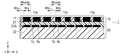
FIG. 1 is a cross-sectional view of an example
schematic configuration of an optical display body
according to an embodiment of the present invention.
An optical display body 1 is configured by stacking a
stripe mask 10 and a printed body 20.
The stripe mask 10 includes a stripe layer 11 in which
linear transmission parts T and reflection parts R
extending in the Y direction are alternately arranged in
the X direction in the drawing, thereby forming a stripe
pattern.
The transmission part T can be the stripe layer 11 as
it is, or can be, for example, a transparent reflection
Date Recue/Date Received 2021-04-16
CA 03116826 2021-04-16
- 13 -
layer. In other words, the transparent reflection layer can
be the transmission part T. When the transparent reflection
layer is taken as the transmission part T, the transmission
part T can be formed by a vacuum film forming method such
as vacuum evaporation or sputtering.
Alternatively, the transmission part T can be a metal
layer having a thickness of less than 20 nm. The metal
layer may be thicker than 5 nm. Material for this metal
layer can be, for example, chromium, nickel, aluminum, iron,
titanium, silver, gold, copper, or an alloy thereof.
For the reflection part R, a metal reflection layer
having a concealing property can be used. In other words,
the metal layer having a concealing property can be the
reflection part R. The reflection part R can be formed by a
vacuum film forming method such as vacuum evaporation or
sputtering. Note that the reflection part R may be printed.
This printing can be performed through gravure printing,
offset printing, or screen printing. An ink for the
printing can be a pigment ink or a dye ink. The ink may
also be pearl ink. Further, the reflection part R may have
a light-scattering property. The light-scattering
reflection part R can be formed through printing, embossing,
or extrusion molding. The light-scattering reflection part
R can be realized by containing a scatterer having an
uneven surface, a low refractive index, or a high
refractive index.
Examples of the material of the metal reflection layer
Date Recue/Date Received 2021-04-16
CA 03116826 2021-04-16
- 14 -
for the reflection part R can include chromium, nickel,
aluminum, iron, titanium, silver, gold, and copper. The
metal reflection layer for the reflection part R typically
has a thickness of from 50 nm to 100 nm. With this
thickness, it is possible to impart a concealing property
appropriate for the stripe mask, and it has excellent
manufacturability.
The stripe layer 11 includes multiple types of stripe
pattern regions that are classified according to a width Wt
of the transmission part T in the X direction. In FIG. 1,
two types of a stripe pattern region ha and a stripe
pattern region lib are illustrated as an example.
The stripe pattern region ha is a region in which the
transmission part T has a smaller width Wt in the X
direction, and the stripe pattern region lib is a region in
which the transmission part T has a larger width Wt in the
X direction. That is, when the transmission part T in the
stripe pattern region lla is taken as a transmission part
Ta and the transmission part T in the stripe pattern region
llb is taken as a transmission part Tb, a width Wta and a
width Wtb have a relationship of Wta < Wtb.
However, in any stripe pattern region 11, the width Wt
of the transmission part T in the X direction is smaller
than the width Wr of the reflection part R in the X
direction, and a relationship of Wt < Wr holds.
Further, regardless of the type of the stripe pattern
region 11, a total width Wtotal (hereinafter, also referred
Date Recue/Date Received 2021-04-16
CA 03116826 2021-04-16
- 15 -
to as "a stripe pitch") of a width Wt of the transmission
part T in the X direction and a width Wr of its adjacent
reflection part R in the X direction is constant in the
region. Therefore, a total width Wtotala (a stripe pitch of
the stripe pattern region 11a) of the width Wta of the
transmission part Ta in the X direction and a width Wra of
its adjacent reflection part Ra in the X direction in the
stripe pattern region 11a, and a total width Wtotalb (a
stripe pitch of the stripe pattern region 11b) of the width
Wtb of the transmission part Tb in the X direction and a
width Wrb of its adjacent reflection part Rb in the X
direction in the stripe pattern region lib have the
following relationships:
Wta + Wra = Wtotala;
Wtb + Wrb = Wtotalb; and
Wtotala = Wtotalb.
Note that although FIG. 1 illustrates only two stripe
pattern regions ha and one stripe pattern region 11b, the
number, size, and layout of the stripe pattern region ha
and the stripe pattern region llb arranged in the stripe
mask 10 can be optionally designed, provided that the
relationships of Wta Wtb, Wt < Wr, Wta + Wra = Wtotala,
Wtb + Wrb = Wtotalb, and Wtotala = Wtotalb are maintained.
Further, although FIG. 1 illustrates only two types of
the stripe pattern region, ha and 11b, the stripe layer 11
can include three or more types of the stripe pattern
region.
Date Recue/Date Received 2021-04-16
CA 03116826 2021-04-16
- 16 -
The stripe layer 11 is translucent and typically
transparent. Material of the stripe layer 11 can be, for
example, a film or sheet made of resin; material of the
resin can be, for example, polyethylene terephthalate (PET),
polypropylene (PP), polycarbonate (PC),
polymethylmethacrylate (PMMA), polyethylene (PE), or the
like.
The stripe layer 11 can also include a diffraction
structure such as at least one of a hologram or a
diffraction grating. For example, a relief structure can be
provided as the diffraction structure on the surface of a
transparent resin forming the stripe layer 11. This allows
a more complicated display; for example, it is possible to
superimpose an image displayed through the diffraction
structure on a latent image or a visible image to be
described later or to arrange them side by side. This
complicated display can enhance the difficulty in
counterfeiting.
When the stripe layer 11 includes the diffraction
structure, material of the stripe layer 11 can be a curable
resin or a thermoplastic resin. Examples of the curable
resin that cures through light can be acrylics,
fluoroacrylics, silicone acrylics, epoxy acrylates,
methylstyrenes, and fluorene polymers. Examples of the
curable resin that cures through heat include thermosetting
resins such as acrylonitrile styrene copolymers, phenols,
melamines, urea resins, and alkyd resins. Examples of the
Date Recue/Date Received 2021-04-16
CA 03116826 2021-04-16
- 17 -
thermoplastic resin include polycarbonate, polypropylene,
polyethylene terephthalate, polystyrene, cycloolefin
polymers, and polyacetals. The diffraction structure can be
formed on the surface of a release layer by shaping the
above resin into a desired structure and then subjecting it
to curing.
Note that the cured resins forming the diffraction
structure are all transparent to light and commonly have a
refractive index of about 1.5; the refractive index can be
greater than 1.4 and less than 1.65.
The printed body 20 is formed of a carrier 22 and a
flattened design layer 21 formed on the carrier 22. The
flattened design layer 21 is composed of material having a
decent adhesion to the carrier 22.
The flattened design layer 21 can be a film or sheet
made of resin. Material of the flattened design layer 21
can be polyethylene terephthalate (PET), polypropylene (PP),
polycarbonate (PC), polymethylmethacrylate (PMMA),
polyethylene (PE), or the like.
FIG. 2 is a plan view for explaining an example of the
flattened design layer 21.
In the flattened design layer 21, as shown in FIG. 2,
a flattened design 21A that is the visible image flattened
in the Y direction in the figure is printed two or more
times repeatedly in the X direction in the figure.
FIG. 3 is a plan view of a visible image that is a
design before flattening for a single flattened design
Date Recue/Date Received 2021-04-16
CA 03116826 2021-04-16
- 18 -
illustrated in FIG. 2.
For example, when a visible image 21B is the
characters "JP" as shown in FIG. 3, the single flattened
design 21A shown in FIG. 2 is a "JP" that is flattened in
the Y direction. As described above, in the flattened
design layer 21, the flattened design 21A that is the
visible image such as a "JP" flattened in the Y direction
is printed two or more times repeatedly in the X direction.
Note that the visible image 21B is not limited to a
character or a design and can be a code related to an owner.
The flattened design 21A can be composed of a dye and
a pigment. In this case, for the formation of the flattened
design 21A, a thermal transfer recording method with a
thermal head, a printing method such as an inkjet recording
method, an electrophotographic method, or a combination of
two or more thereof can be used. Alternatively, the
flattened design 21A can be formed by drawing with a laser
beam on a layer containing a thermosensitive color former.
Alternatively, a combination of these methods can be used.
The flattened design 21A can consist only of, for
example, black ink. Alternatively, the flattened design 21A
can be composed of an ink in any one or more colors of cyan,
yellow, or magenta.
When the flattened design 21A is composed of inks in
any two or more colors of cyan, yellow, or magenta, it is
desirable that the inks of two or more colors be shaped
into dots that overlap in a predetermined area. In this
Date Recue/Date Received 2021-04-16
CA 03116826 2021-04-16
- 19 -
case, it is difficult to copy the printed body with a color
copier or the like, which can enhance the anti-
counterfeiting and anti-falsification effects.
Material of the carrier 22 can be, for example, paper.
The material of the carrier 22 can also be, for example, a
plastic substrate, a metal substrate, a ceramic substrate,
or a glass substrate.
FIG. 4 is a cross-sectional view of another example
schematic configuration of the optical display body
according to the embodiment of the present invention.
The optical display body 2 shown in FIG. 4 has the
stripe mask 10 and the printed body 20 separated. In such a
case, the stripe mask 10 includes a transparent carrier 12
in addition to the stripe layer 11 described with reference
to FIG. 1. The printed body 20, on the other hand, includes
the flattened design layer 21 and the carrier 22 as in the
configuration described with reference to FIG. 1.
In FIG. 4, the stripe mask 10 is the same as that in
FIG. 1 except that the transparent carrier 12 is included;
thus, a difference from FIG. 1 will be described below to
avoid redundant descriptions.
The transparent carrier 12 has a light transmission
property and is typically transparent. The transparent
carrier 12 can be a plastic film or a plastic sheet.
Material of the transparent carrier 12 can be polyethylene
terephthalate (PET), polypropylene (PP), polycarbonate (PC),
polymethylmethacrylate (PMMA), or polyethylene (PE).
Date Recue/Date Received 2021-04-16
CA 03116826 2021-04-16
- 20 -
FIGS. 5 and 6 are example plan views of the stripe
mask 10 in which a design defined by a boundary of the
stripe pattern region ha and the stripe pattern region llb
is formed.
As illustrated in FIGS. 5 and 6, when the arrangement
of the stripe pattern region ha and the stripe pattern
region llb is changed with their stripe directions kept
coincident with the X direction in the stripe mask 10, the
shape defined by the boundary between the pattern region
ha and the pattern region llb also changes.
Further, the proportion between the transmission part
T and the reflection part R in the stripe pitch Wtotal is
different between the stripe pattern region ha and the
stripe pattern region 11b. That is, the stripe mask 10 can
include regions having different proportions between the
transmission part T and the reflection part R. In this case,
the stripe pattern region ha and the stripe pattern region
llb have different reflected-light intensity distributions
for light. By utilizing this difference in reflected-light
intensity distribution, the shape defined by the boundary
between the stripe pattern region ha and the stripe
pattern region llb can be made to manifest as a latent
image on the XY plane of the stripe mask 10.
FIGS. 5 and 6 both show examples in which a cross
shape is defined in the center; however, FIG. 5 shows the
cross shape defined by the stripe pattern region llb being
arranged around the stripe pattern region 11a, while FIG. 6
Date Recue/Date Received 2021-04-16
CA 03116826 2021-04-16
- 21 -
shows the cross shape defined by the stripe pattern region
ha being arranged around the stripe pattern region 11b. In
such a case, the cross shape manifests as a bright cross-
shaped latent image Li in FIG. 5, while it manifests as a
dark cross-shaped latent image L2 in FIG. 6.
FIG. 7 is a conceptual diagram for explaining a
viewing angle range in which a latent image L can be
visually confirmed.
FIG. 8 is a conceptual diagram illustrating the latent
image L that is visually confirmed. The stripe mask 10 can
visualize the latent image L. The stripe mask 10 serves as
a visible image filter. The visible image filter visualizes
the latent image L.
As shown in FIG. 7, the latent image L, upon being
observed from a viewing angle range a (for example, 20 to
400 from the surface of the stripe mask 10) that is acute
with respect to the face of the stripe mask 10, is well
visually confirmed as shown in FIG. 8.
FIG. 9 is a conceptual diagram for explaining a
positional relationship between the stripe mask and the
printed body in the XY plane.
The optical display body 1 is configured by
superimposing the stripe mask 10 and the printed body 20
such that the stripe direction (X direction) of the stripe
mask 10 and the X direction of the printed body 20 coincide
with each other.
By the stripe mask 10 thus being superimposed on the
Date Recue/Date Received 2021-04-16
CA 03116826 2021-04-16
- 22 -
printed body 20 that includes the flattened design layer 21
in which multiple flattened designs 21A are regularly
arranged, the visible image 21B that can be visually
confi/med manifests. The mechanism of such a manifestation
of the visible image 21B will be explained as follows. The
visible image 21B is an image in which the latent image
manifests.
FIGS. 10 and 11 are conceptual diagrams showing in
detail positional relationships between the stripe mask and
the printed body in the XY plane in order to explain the
mechanism through which the visible image manifests.
FIG. 10 shows the stripe mask 10 illustrated in FIG. 6,
and FIG. 11 shows the stripe mask 10 illustrated in FIG. 5.
Further, in both FIGS. 10 and 11, the flattened design 21A
as illustrated in FIG. 2 is placed in the flattened design
layer 21 of the printed body 20. The flattened design 21A
is, for example, black ink that is thermally transferred
into a predetermined size, for example, into a dot shape;
alternatively, any one or more colors of cyan, yellow, or
magenta may be thermally transferred into a predetermined
size.
In the stripe mask 10 shown in FIGS. 10 and 11, the
stripe pitch Wtotal (Wtotal = Wtotala = Wtotalb) is
designed to differ from an integral multiple of an
arrangement pitch P in which the flattened design 21A is
repeatedly arranged in the X direction in the printed body
20. That is, the relationship of Wtotal 0 nP (n is a
Date Recue/Date Received 2021-04-16
CA 03116826 2021-04-16
- 23 -
positive integer) holds. Typically, the stripe pitch Wtotal
can have a deviation amount of 10% or more and 25% or
less with respect to the arrangement pitch P.
The stripe pitch Wtotal differing from the integral
multiple of the arrangement pitch P allows the visible
image 21B to manifest. This mechanism will be explained
using FIGS. 12 and 13.
FIGS. 12 and 13 are enlarged views of part of the
printed body with the stripe mask superimposed thereon in
order to schematically explain the mechanism for the
manifestation of the visible image.
FIG. 12(a) and FIG. 13(a) are plan views illustrating
a single flattened design 21A that is placed in the
flattened design layer 21. FIG. 12(a) and FIG. 13(a), for
the sake of explanation, illustrate the flattened design
21A having a design different from that illustrated in
FIG. 2.
FIG. 12(b) and FIG. 13(b) are plan views showing the
positional relationship between the flattened designs 21A
arranged in the X and Y directions at their respective
equal pitches on the flattened design layer 21, and the
transmission part T of the superimposed stripe mask 10.
FIG. 12(c) and FIG. 13(c) are plan views showing the
positional relationship between flattened designs 21A
arranged in the X and Y directions at their respective
equal pitches on the flattened design layer 21, and the
reflection part R of the superimposed stripe mask 10.
Date Recue/Date Received 2021-04-16
CA 03116826 2021-04-16
- 24 -
In the example shown in FIG. 12, the stripe pitch
Wtotal is greater than the arrangement pitch P within the
range of from +10% to 25%; in the example shown in FIG. 13,
the stripe pitch Wtotal is less than the arrangement pitch
P within the range of from -10% to 25%.
When the stripe pitch Wtotal is greater than the
arrangement pitch P, the stripe mask 10 upon being
superimposed on the printed body 20 allows the visible
image 213 before flattening to manifest as shown by a
dotted line in FIG. 12(c). On the other hand, when the
stripe pitch Wtotal is less than the arrangement pitch P,
the stripe mask 10 upon being superimposed on the printed
body 20 allows the visible image 21B before flattening to
manifest as shown by a dotted line in FIG. 13(c).
In this manner, the manifestation of the visible image
213 before flattening results from the difference between
the arrangement pitch P and the stripe pitch Wtotal, which
difference causes a site of the flattened design 21A that
is observed through the transmission part T of the stripe
mask 10 to gradually shift along the X direction in the
flattened designs 21A repeatedly arranged in the X
direction on the flattened design layer 21. By masking part
of the flattened designs 21A with the stripe mask 10 in
this manner, the visible image 21B before flattening
manifests.
Parallel lines for the visualization may include
regions with different stripe pitches Wtotal. The parallel
Date Recue/Date Received 2021-04-16
CA 03116826 2021-04-16
- 25 -
lines may include a plurality of regions having different
stripe pitches Wtotal with respect to the arrangement pitch
P of the visible image 21B. Thereby, the visible image 21B
to be displayed through the parallel lines changes
according to the regions.
Further, as an example of this, the parallel lines may
include a region where the stripe pitch Wtotal of the
parallel lines has a longer pitch than the arrangement
pitch P of the visible image 21B, and a region where the
stripe pitch Wtotal of the parallel lines has a longer
pitch than the arrangement pitch P of the visible image 21B.
In this case, even when the visible image 21B is the same,
the difference in the region for the visualization can
invert the image 21B through the difference in the region
for visualization of the parallel lines.
Such visualization is highly discriminating and
characteristic, and thus has a high anti-counterfeiting
effect. Further, the outer shape of the region may be
visible information, and the visible information may be
numbers, characters, signs, or symbols. This outer shape
can attain highly discriminating visualization information
and can further enhance the anti-counterfeiting.
FIG. 14 is a conceptual diagram for explaining a
viewing angle range in which a visible image can be
visually confirmed.
FIG. 15 is a conceptual diagram illustrating a visible
image visually confirmed.
Date Recue/Date Received 2021-04-16
CA 03116826 2021-04-16
- 26 -
As shown in FIG. 14, the visible image, upon being
observed from a viewing angle range p (for example, an
angle range of 50 from the normal direction with respect
to the stripe mask 10) centered on the front direction of
the stripe mask 10, can be well visually confirmed as shown
in FIG. 15. This viewing angle range p can be made not to
overlap with the viewing angle range a shown in FIG. 7. In
this case, the ability to be visually confirmed can be
improved.
Note that depending on the magnitude relationship
between the arrangement pitch P and the stripe pitch Wtotal,
a vertical relationship of the pre-flattening visible image
21B that is to be manifest is reversed in the X direction.
That is, when the stripe pitch Wtotal is greater than the
arrangement pitch P, the flattened design 21A and the
visible image 21B before flattening have the same vertical
relationship as shown in FIG. 12(c); however, when the
stripe pitch Wtotal is less than the arrangement pitch P,
the vertical relationship between the flattened design 21A
and the visible image 21B before flattening is reversed as
shown in FIG. 13(c).
When the stripe pitch Wtotal is equal to an integral
multiple of the arrangement pitch P (that is, when the
relationship of Wtotal = nP holds, where n is a positive
integer), the visible image 213 before flattening will not
manifest even if the stripe mask 10 is superimposed on the
printed body 20. This is because the sites in the flattened
Date Recue/Date Received 2021-04-16
CA 03116826 2021-04-16
- 27 -
designs 21A observed through the transmission part T of the
stripe mask 10 will be all the same along the X direction
in the flattened designs 21A repeatedly arranged in the X
direction on the flattened design layer 21.
A typical stripe pitch Wtotal of the stripe mask 10 is
from 250 pm to 500 pm. Further, an example of the width Wta
of the transmission part Ta of the stripe pattern region
ha in the X direction is from 30 pm to 70 pm, and the
width Wtb of the transmission part Tb of the stripe pattern
region lib in the X direction is, as an example, from 70 pm
to 120 pm. A proportion of a portion of the stripe pattern
region lla that is concealed by the reflection part Ra in
the entire stripe mask 10 is small, and the visible image
21B before flattening can be visually confirmed with ease
from the flattened design 21A of the printed body 20. The
area of the flattened design 21A partially shown through
the transmission part Tb of the stripe pattern region lib
is small, which makes it easy to visualize the flattened
design 21A.
If the width Wta of the transmission part Ta of the
stripe pattern region ha in the X direction is less than
pm, a proportion of a portion of the stripe pattern
region lla that is concealed by the reflection part Ra in
the entire stripe mask 10 would increase, which makes it
25 difficult to visually confirm the visible image 21B from
the flattened design 21A of the printed body 20.
Further, if the width Wtb of the transmission part Tb
Date Recue/Date Received 2021-04-16
CA 03116826 2021-04-16
- 28 -
of the stripe pattern region llb in the X direction is made
greater than 120 pm, the area of the flattened design 21A
partially shown through the transmission part Tb of the
stripe pattern region llb would be wider, which in turn
makes it difficult to visualize the visible image 21B
before flattening.
A typical arrangement pitch P of the flattened design
21A is from 250 pm to 500 pm. Within this range, it is easy
to express details about the code related to the owner,
which can reduce the risk of counterfeiting or
falsification.
If the arrangement pitch P is less than 250 pm, it
would be difficult for the flattened design 21A to express
details about characters, patterns, or codes related to the
owner. Further, if the arrangement pitch P is larger than
500 pm, the resolution of the stripe mask 10 would
inevitably tend to be coarse so as to correspond to the
flattened design 21A. This will increase the risk of
counterfeiting or falsification and thus is not preferable.
As described above, in the optical display body
according to the embodiment of the present invention,
through the mechanism as described above, when the stripe
mask 10 is viewed from the front side, the visible image M
can be visually confirmed as shown in FIG. 15, and when the
stripe mask 10 is viewed from an oblique side, the latent
image L can be visualized as shown in FIG. 8. In this
manner, it is possible to switch the types of the image
Date Recue/Date Received 2021-04-16
CA 03116826 2021-04-16
- 29 -
that can be visually confirmed according to the viewing
angle range, which can enhance the anti-counterfeiting
effect.
(Modification 1)
Next, modification 1 of the optical display body
according to the embodiment of the present invention will
be described.
In modification 1 of the optical display body
according to the embodiment of the present invention, the
optical display body provided with an adhesive layer as
appropriate will be described.
FIG. 16 is a cross-sectional view of an example of
modification 1 of the optical display according to the
embodiment of the present invention.
The optical display body 3 illustrated in FIG. 16 is
an example modification of the optical display body 1
illustrated in FIG. 1 and differs from the optical display
body 1 in that an adhesive layer 15 is provided between the
flattened design layer 21 and the carrier 22 in the printed
body 20. Therefore, hereinafter, only the difference from
the optical display body 1 will be described and redundant
descriptions will be omitted.
That is, in the optical display body 3, the flattened
design layer 21 and the carrier 22 are bonded to each other
by the adhesive layer 15. In order to increase the adhesion,
the carrier 22 can be provided with an adhesive anchor
layer (not shown) so that the adhesive layer 15 can be
Date Recue/Date Received 2021-04-16
CA 03116826 2021-04-16
- 30 -
provided on the adhesive anchor layer. The adhesive anchor
layer may serve as the adhesive layer 15.
Further, as shown in FIG. 4, in the optical display
body 2 having the stripe mask 10 and the printed body 20
separated, the adhesive layer can also be provided in order
to increase the adhesion between the stripe layer 11 and
the transparent carrier 12. In this case, an adhesive
anchor layer (not shown) can be provided on the transparent
carrier 12, and an adhesive layer can be formed on the
adhesive anchor layer to bond the stripe layer 11 to the
transparent carrier 12.
Further, the flattened design 21A can be formed
directly on the stripe layer 11 not on the flattened design
layer 21 through thermal transfer using a thermal head. In
this case, the stripe layer 11 can be formed of, for
example, the same material as that of the flattened design
layer 21. An adhesive anchor layer or an adhesive layer can
be provided on the face on a printing side of the stripe
layer 11 in order to increase the adhesion.
As described above, the adhesive layer 15 and/or the
adhesive anchor layer can be provided for the optical
display body 1 or 2 illustrated in FIG. 1 or 4 as
appropriate.
(Modification 2)
Next, modification 2 of the optical display body
according to the embodiment of the present invention will
be described.
Date Recue/Date Received 2021-04-16
CA 03116826 2021-04-16
- 31 -
In modification 2 of the optical display body
according to the embodiment of the present invention, the
optical display body in which the surface of the stripe
layer 11 is covered with the transparent carrier 12 will be
described.
FIG. 17 is a cross-sectional view of an example of
modification 2 of the optical display body according to the
embodiment of the present invention.
The optical display body 4 illustrated in FIG. 17 is
an example modification of the optical display body 2
illustrated in FIG. 4 and differs from the optical display
body 2 in that the stripe mask 10 is composed of the stripe
layer 11 and the transparent carrier 12 covering the
surface of the stripe layer 11. Therefore, hereinafter,
only the difference from the optical display body 2 will be
described and redundant descriptions will be omitted.
The transparent carrier 12 is for protecting the
surface structure of the stripe layer 11, has a light
transmission property, and is typically transparent. The
transparent carrier 12 is composed of, for example, a film
or sheet made of resin, and examples of material of the
resin include polyethylene terephthalate (PET),
polypropylene (PP), polycarbonate (PC),
polymethylmethacrylate (PMMA), and polyethylene (PE).
In the manner described above, the transparent carrier
12 for protecting the surface structure of the stripe layer
11 can be provided.
Date Recue/Date Received 2021-04-16
CA 03116826 2021-04-16
- 32 -
The optical display body according to the embodiment
of the present invention described above can be applied to
a product as a security medium for anti-counterfeiting or
anti-falsification. The product can be a printed product.
The printing can be performed through gravure printing,
offset printing, or screen printing. The printed product
applied as a security medium can serve as a security print.
The security print copes with both anti-counterfeiting
and/or anti-falsification and aesthetics. The printed
product is, for example, a passport, a card, a bill, a tag,
a label, or a ticket. The card can serve as an ID card. The
ID card has identification information recorded thereon as
either electronic or visible information or as both. The
identification information can be biometric information or
non-biometric information. Examples of the biometric
information include personal signatures, facial photographs,
portraits, fingerprints, irises, and a combination thereof.
Examples of the non-biometric information include
individual names, nationalities, genders, addresses,
affiliations, and a combination thereof. Therefore,
application of the above embodiment to actual products will
be described as implementations below.
[Implementation 11
In this implementation, an example of applying the
optical display body to a passport booklet or a card will
be described.
FIG. 18 is a top view (a) and a perspective view (b)
Date Recue/Date Received 2021-04-16
CA 03116826 2021-04-16
- 33 -
schematically showing an example plane structure of a
passport booklet 40 on which the optical display body 3
shown in FIG. 16 is placed.
FIG. 19 is a top view (a) and a perspective view (b)
schematically showing an example plane structure of an ID
card 46, which is an example card on which the optical
display body 3 shown in FIG. 16 is placed.
As illustrated in FIG. 18, the passport booklet 40 is
composed of a cover 42, a data page 44, a VISA page (not
shown), and the like.
As illustrated in FIG. 19, the ID card 46 is composed
of a data page 44 similar to that in the passport booklet
40 illustrated in FIG. 18.
Although the specifications of the data page 44 vary
from country to country, the data page 44 illustrated in
FIGS. 18 and 19 is formed by coating a page made of paper
with a transparent adhesive layer and then placing thereon
the optical display body 3, as illustrated in FIG. 16,
through thermal transfer.
Note that in the portion of the data page 44 where the
optical display body 3 is placed, the paper substrate can
be replaced with a plastic substrate, a metal substrate, a
ceramic substrate, or a glass substrate.
Hot stamping can be applied to the thermal transfer.
Alternatively, a thermal roll or a thermal head instead of
the hot stamping can be used to perform the thermal
transfer.
Date Recue/Date Received 2021-04-16
CA 03116826 2021-04-16
- 34 -
Further, at the time of the thermal transfer, an
adhesive anchor layer can be formed on the substrate of the
data page 44 as appropriate in order to increase the
adhesion. When bonding to the carrier 22 of the optical
display body 3 is difficult with high adhesion, the thermal
transfer can be performed via the adhesive layer as
appropriate.
Personal information such as a name, an expiration
date, and a face photograph is recorded on the data page 44.
In this implementation, a passport printer (eP600
manufactured by Toppan Printing Co., Ltd.) was used to
record the name, expiration date, face photograph, and
flattened design 21A. Hereinafter, this recording process
will be described.
First, the visible image 21B (for example, the
characters "JP" shown in FIG. 3) to be visualized was
prepared and enlarged in its breadth by five times using
image processing software (Adobe Photoshop), thereby
obtaining a flattened design 21A.
Next, an intermediate transfer medium was prepared as
the stripe layer 11. As the intermediate transfer medium, a
medium composed of a base film, a release/protective layer,
and a picture/adhesive layer was used. Then, the stripe
pattern regions ha and lib were arranged in a part of the
picture/adhesive layer so as to form a cross shape at the
center, as shown in, for example, FIG. 6.
The stripe pitch Wtotal of the stripe pattern regions
Date Recue/Date Received 2021-04-16
CA 03116826 2021-04-16
- 35 -
11a and lib was 425 pm, the width Wra of the reflection
part Ra of the stripe pattern region ha in the X direction
was 385 pm, and the width Wrb of the reflection part Rb of
the stripe pattern region 11b in the X direction was 340 pm.
The width Wr of the reflection part R was realized by
demetallizing the evaporated aluminum.
A transfer ribbon was superimposed on the region of
the intermediate transfer medium where the evaporated
aluminum was demetallized, and a recorded image was formed
using a thermal head.
Specifically, first, information such as a name and an
expiration date and the flattened design 21A obtained as
described above were transferred with black ink, and then
cyan, magenta, and yellow inks were sequentially
transferred in the face photograph. Note that the
arrangement pitch P of the flattened design 21A in the
direction (the X direction in FIG. 2) orthogonal to the
flattening direction (the Y direction in FIG. 2) was set to
380 pm, which was about 11% less than the stripe pitch
Wtotal.
Next, the intermediate transfer medium on which the
image was recorded was superimposed on the data page 44 and
thermally transferred using a heat roller.
FIG. 20 is a schematic diagram showing an example
visible image M observed when the data page 44 shown in
FIGS. 18 and 19 is viewed from its front side.
When the data page 44 shown in FIGS. 18 and 19 was
Date Recue/Date Received 2021-04-16
CA 03116826 2021-04-16
- 36 -
viewed from the front side, the visible image 21B (the
characters "JP" illustrated in FIG. 12) could be visually
confirmed as the visible image M as shown in FIG. 20; and
when the data page 44 was viewed from the oblique side, the
cross-shaped latent image L could be visually confirmed as
shown in FIGS. 18(b) and 19(b).
In this manner, it was confirmed that since the image
to be visually confirmed can be selectively switched by
changing an angle to observe the stripe mask 10, the
security can further improve.
In this manner, it was confirmed that the security of
the passport booklet or ID card is improved by placing the
optical display body on the passport booklet or ID card.
[Implementation 2]
In implementation 1, there has been described the
example where the optical display body having the stripe
mask 10 and the printed body 20 integrated as shown in
FIG. 16 was applied and the optical display body was
integrally placed on a single object such as the data page
44.
In implementation 2, as shown in FIGS. 4 and 17, there
will be described an example page pair where the optical
display body having the stripe mask 10 and the printed body
20 separated was applied and the optical display body was
integrally placed on each page.
FIG. 21 is a conceptual diagram showing an example
configuration of a page pair in which a stripe mask and a
Date Recue/Date Received 2021-04-16
CA 03116826 2021-04-16
- 37 -
printed body are placed on different pages.
In a page pair 50, a page 52 on which the stripe mask
is placed and a page 54 on which the printed body 20 is
placed are paired. The page 52 and the page 54 are bound
5 together at a center line 56 by gluing or the like. The
center line 56 is also used as a folding line for such
folding that the page 52 and the page 54 are superimposed
on each other.
FIG. 22 is a conceptual diagram showing another
10 example configuration of the page pair.
The page pair 50 is not limited to the configuration
in which the page 52 and the page 54 are composed of
individual faces that are originally separated, as shown in
FIG. 21, and the page 52 and the page 54 may be composed of
the same face 58 as shown in FIG. 22. That is, the page
pair 50 shown in FIG. 22 is configured such that the same
face 58 made of, for example, paper can be folded at the
center line 56. Thereby, for example, taking the center
line 56 as the boundary, the right side in the figure can
be regarded as the page 52 and the left side in the figure
as the page 54.
Although paper can be used for the pages 52 and 54,
for example, a plastic substrate, a metal substrate, a
ceramic substrate, or a glass substrate in addition to
paper can be used.
In such a page pair 50, the stripe mask 10 was placed
on the page 52 in the manner described below.
Date Recue/Date Received 2021-04-16
CA 03116826 2021-04-16
- 38 -
First, on the page 52, at least the region where the
stripe mask 10 was placed was made transparent.
Next, the stripe mask 10 was attached to the surface
of the page 52 via an adhesive layer.
FIG. 23 is a conceptual diagram showing an example
page pair in which a stripe mask is placed on a transparent
page.
As another way of placing the stripe mask 10 on the
page 52, the stripe mask 10 can be transferred to the
surface of the page 52 under predetermined pressure and
heat. Also, the stripe mask 10 can be placed on the page 52
by sandwiching the stripe mask 10 with carriers (not shown)
of the page 52 or embedding the stripe mask 10 in the
carrier. When the stripe mask 10 is sandwiched between the
carriers of the page 52, the page 52 is provided with a
through hole having an area smaller than the area of the
stripe layer 11 at a site where the stripe layer 11 is
placed, and the stripe layer 11 is placed so as to close
the through hole.
Next, the printed body 20 was placed on the page 54.
In this case, the printed body 20 was placed on the page 54
by adjusting the placement position such that the page 52
and the page 54, when folded along the center line 56 as
shown in FIG. 24, will be superimposed with the stripe
direction (X direction) of the stripe layer 11 and the X
direction of the printed body 20 coincident with each other.
FIG. 24 is a side view of the page 52 and the page 54
Date Recue/Date Received 2021-04-16
CA 03116826 2021-04-16
- 39 -
folded along the center line 60.
FIG. 25 is a schematic diagram showing an example
visible image observed when a data page is viewed from its
front side.
FIG. 26 is a schematic diagram showing an example
latent image observed when a data page is viewed from its
oblique side.
When the stripe layer 11 is observed from its front
side in a state where the page pair 50 is folded along the
central line 56 such that the page 52 and the page 54 are
superimposed as shown in FIG. 24, the visible image 21B
(the characters "JP") before flattening can be visually
confirmed as the visible image 21B, as shown in FIG. 25.
Further, when the stripe layer 11 is observed from an
oblique direction, the cross-shaped latent image L can be
visually confirmed as shown in FIG. 26.
Note that when the stripe layer 11 is observed from an
oblique direction with the page 52 and the page 54 not
superimposed, that is, with the page 52 and the page 54
open as well, the cross-shaped latent image L can be
visually confirmed, as shown in FIG. 26.
As described above, it was confirmed that the security
of the page pair 50 can be improved by placing the optical
display body having the stripe mask 10 and the print body
20 separated on the page pair 50.
[Implementation 3]
In this implementation, application of the optical
Date Recue/Date Received 2021-04-16
CA 03116826 2021-04-16
- 40 -
display body to a label and/or a tag will be described.
FIG. 27 is a cross-sectional view showing a
configuration of a label 1 configured by providing an
adhesive layer on the optical display body shown in FIG. 1.
The optical display body 1 included in the label 60 is
configured to allow a character, a pattern, or a code
relating to the owner to manifest through the mechanism as
described above.
FIGS. 28 and 29 are plan views schematically showing
an example tag to which the label shown in FIG. 27 is
attached.
The tag 62 as shown in FIGS. 28 and 29 is configured
by attaching the label 60 shown in FIG. 27 via the adhesive
layer 30.
The substrate of the tag 62 to which the label 60 is
attached can be a cloth substrate, a paper substrate, a
plastic substrate, a metal substrate, a ceramic substrate,
or a glass substrate.
As a result, when viewed from the front side, the
visible image 21B such as "JP" was confirmed as the visible
image M as shown in FIGS. 28(a) and 29(a), and when viewed
from the oblique side, the latent image L was observed as
shown in FIGS. 28(b) and 29(b).
Further, a tag attachment region 64 can be processed
to be provided with a round hole 66 as shown in FIG. 28.
Further, the label can be sewn directly onto a product as
shown in a sewing line 68 of FIG. 29.
Date Recue/Date Received 2021-04-16
CA 03116826 2021-04-16
- 41 -
In the manner described above, it was confirmed that
even when the optical display body 1 was applied to the
label 60 or the tag 62, the image to be visually confirmed
can be selectively switched by changing an angle for the
observation, and the security thus can be improved.
Therefore, it was also confirmed that the label 60 or
the tag 62 can be applied to the authenticity determination
of a product by, for example, attaching to or being sewn on
a product.
The present invention is not limited to the above-
described embodiments, and can be modified in practice,
without departing from the gist of the invention. In
addition, embodiments may be combined as appropriate, in
which case a combined effect is obtained. Furthermore, the
above-described embodiments include various inventions, and
various inventions can be extracted by an appropriate
combination of structural elements selected from a
plurality of disclosed structural elements.
Date Recue/Date Received 2021-04-16