Note: Descriptions are shown in the official language in which they were submitted.
CA 03116905 2021-04-16
WO 2020/092688 PCT/US2019/059027
EFFICIENT PRODUCTION OF NANOFIBER STRUCTURES
RELATED APPLICATIONS
This application claims the benefit of priority to U.S. Provisional Patent
Application
serial number 62/754,183, filed November 1, 2018, which is hereby incorporated
by
reference in its entirety.
BACKGROUND
Electrospinning is a fiber production method in which an electric force is
applied to
a polymer solution present at a spinning electrode. The application of the
electric field pulls
a charged thread of the solution from the spinning electrode towards a
collecting electrode.
This thread of polymer solution dries in flight, forming a fiber that is
deposited on a
substrate typically positioned at the collecting electrode. Depending upon the
specific
parameters applied to the electrospinning process, the produced fibers can
have diameters
ranging from a few nanometers up to several micrometers.
Electrospinning apparatuses are designed to adjust the position of the
substrate and
collector simultaneously. Most electrospinning studies utilize a grounded
collector which
serves both as the counter electrode and as the collecting substrate. This
design makes it
impossible to decouple the impacts of substrate distance vs. electric field
strength, limiting
the ability to independently test the effect of changes in these distances on
electrospinning
efficiency. Since the interelectrode gap needs to be maintained at a safe
distance to prevent
electrical discharge, especially at higher voltages, lower substrate distances
have not been
investigated as an independent variable.
SUMMARY
Provided herein are electrospinning apparatuses and methods of producing
nanofiber structures with increased productivity (e.g., nanofiber mats).
In certain aspects, provided herein are electrospinning apparatuses that
comprise: (a)
a spinning electrode; (b) a substrate that is a first distance from the
spinning electrode (the
substrate distance); and (c) a collecting electrode that is a second distance
from the spinning
electrode (the interelectrode distance), wherein the substrate is positioned
between the
spinning electrode and the collecting electrode. In some embodiments, the
ratio of the
substrate distance to the interelectrode distance is less than 1 (e.g., no
greater than 0.77).
- 1 -
CA 03116905 2021-04-16
WO 2020/092688 PCT/US2019/059027
In certain aspects, provided herein are electrospinning apparatuses
comprising: (a) a
spinning electrode; (b) a substrate that is a first distance from the spinning
electrode (the
substrate distance); and (c) a collecting electrode that is a second distance
from the spinning
electrode (the interelectrode distance), wherein the apparatus is configured
such that the
substrate distance and the interelectrode distance are separately adjustable
and capable of
being configured such that the ratio of the substrate distance to the
interelectrode distance is
less than 1.0 (e.g., no greater than 0.77).
In certain aspects, provided herein are methods of producing a nanofiber
structure
(e.g., a nanofiber mat) using an electrospinning apparatus provided herein. In
some
embodiments, the method comprises electrospinning a polymer solution from the
spinning
electrode of the apparatus provided herein onto its substrate.
Thus, in certain aspects, provided herein are methods for producing a
nanofiber
structure (e.g., a nanofiber mat) comprising electrospinning a polymer
solution from a
spinning electrode onto a substrate that is positioned between the spinning
electrode and a
collecting electrode, wherein the ratio of the substrate distance to the
interelectrode distance
is less than 1 (e.g., no greater than 0.77).
BRIEF DESCRIPTION OF THE DRAWINGS
Figure 1 shows a schematic depiction of certain conditions applied during the
electrospinning experiments described in Example 1.
Figure 2 is a graph depicting the relationship between substrate distance,
electric
field, basis weight and fiber diameter during exemplary electrospinning
processes.
Figure 3 shows a schematic depiction of certain conditions applied during in
certain
of the electrospinning experiments described in Example 2.
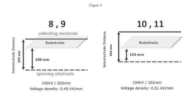
Figure 4 shows a schematic depiction of conditions applied during
electrospinning
experiments described in Example 3 (Production unit). Runs 8 and 9 and well as
10 and 11
have identical experimental conditions. Each of these pairs have a
differentiating line speed.
Figure 5 shows a table summarizing the parameters applied and results obtained
during Experiments 1-11 as set forth in Examples 1-3. "*- normalized by
dividing the
productivity by number of electrodes (i.e., N=8)". The rows with bold letters
are high
productivity settings.
Figure 6 shows the ability of certain embodiments disclosed herein to increase
productivity while maintaining a product unifority. Panel a depicts the
increase in
- 2 -
CA 03116905 2021-04-16
WO 2020/092688 PCT/US2019/059027
productivity per electrode (in g/m-min) achieved by decreasing the substrate
distance while
maintaining a constant electrode distance. Panel b shows that decreasing the
substrate
distance while maintaining a constant electrode distance does not adversely
impact the
count fiber mean diameter of the nanofiber mat produced. The hatched bar graph
in panel b
represents low-distance ratio. Higher productivity is augmented by combination
of
increasing the electric field and decreasing the distance ratio (d-s/d-ie).
Figure 7 shows representative Scanning Electron Microscope (SEM) images of
electrospun nanofiber generated at (a) standard and (b) high productivity
settings using
production equipment. The micrograph shows that comparable fiber structures
were
obtained at both settings.
DETAILED DESCRIPTION
General
Electrospinning is a technique that can produce non-woven fibrous material
with
fiber diameters ranging from tens of nanometers to microns, a size range that
is otherwise
difficult to control by conventional non-woven fiber fabrication techniques.
The quality and
quantity of the fibers produced depend on several parameters. These parameters
include
molecular weight, molecular weight distribution and structure of the polymer;
solution
properties (i.e., viscosity, conductivity, and surface tension); electrical
potential, flow rate,
and concentration; distance between the spinning electrode and the substrate;
environmental
parameters (i.e., temperature, humidity, and air velocity in the chamber);
motion and size of
the collector; and needle gauge.
In certain aspects, provided herein are electrospinning apparatuses that can
produce
uniform nanofibers while improving process productivity without compromising
the
microstructure of the nanofiber mat by reducing the distance between spinning
electrode
and the substrate relative to the distance between the spinning electrode and
the collecting
electrode. Accordingly, the electrospinning apparatuses provided herein
comprise (a) a
spinning electrode; (b) a grounded substrate that is a first distance from the
spinning
electrode (the substrate distance); and (c) a collecting electrode that is a
second distance
from the spinning electrode (the interelectrode distance) wherein, the ratio
of the substrate
distance to the interelectrode distance is no greater than 1 (e.g., less than
0.86). In some
embodiments, the apparatus is configured such that the substrate distance can
be
conveniently adjusted independent of the interelectrode distance (e.g., using
a dial, lever
- 3 -
CA 03116905 2021-04-16
WO 2020/092688 PCT/US2019/059027
and/or button). In certain aspects, provided herein are methods of making an
electrospun
structure, such as an electrospun mat, using an apparatus provided herein.
The productivity improvements provided by the methods and compositions
disclosed herein have implications at the industrial production level. Certain
embodiments
of the methods and compositions provided herein can be used to increase amount
of
material being produced in an existing manufacturing line and, in doing so,
decrease the
production cost of a particular filter structure produced on that line. In
some embodiments
the methods and compositions provided herein can be used to make higher basis
weight
filter structures on an existing manufacturing line without increasing the
production cost
and without reducing the amount of material being produced.
Definitions
For convenience, certain terms employed in the specification, examples, and
appended claims are collected here.
As used herein, the singular forms "a," "an" and "the" are intended to include
the
plural forms as well, unless the context clearly indicates otherwise.
The term "about" means within an acceptable error range for the particular
value as
determined by one of ordinary skill in the art. As used herein, "about" refers
to an amount
that is within 10% of a given value. In other words, these values include the
stated value
with a variation of 0-10% around the value (X 10%).
The terms "variation" and "coefficient of variation" are used interchangeably
herein
and refer to a standardized measure of dispersion of a probability
distribution or frequency
distribution. It is often expressed as a percentage and is defined as the
ratio of the standard
deviation to the mean.
The term "productivity" as used herein is a measure of the quantity of fiber
produced per unit time per unit length of the spinning electrode (g/m-min). In
certain
embodiments, productivity is calculated as the product of the basis weight (g
/ m2) and line
speed (m/min) and is directly related to the process economy.
The term "high productivity settings" as used herein refers to electrospinning
apparatus settings in which the ratio of the substrate distance to the
interelectrode distance
is less than 0.88 (e.g., no greater than 0.75, 0.70, 0.65, 0.60. 0.55, 0.50,
etc.). In some
embodiments high productivity settings are applied in combination with the use
of a high
electric field (e.g., an electric field of at least 0.7 kV/mm).
- 4 -
CA 03116905 2021-04-16
WO 2020/092688 PCT/US2019/059027
The term "polymer" refers to a relatively high molecular weight organic
compound,
natural or synthetic, whose structure can be represented by a repeated small
unit, the
monomer (e.g., polyethylene, rubber, cellulose). Synthetic polymers are
typically formed by
addition or condensation polymerization of monomers. Polymers that are
suitable for use in
the nanofiber substrate layer of the invention include, but are not limited
to,
polyethersulfones, polysulfones, polyimides, polyvinylidene fluorides,
polyethylene
terephthalates, polybutylene terephthalates, polypropylene terephthalates,
polypropylenes,
polyethylenes, polyacrylonitriles, polyamides, and polyaramids.
The term "nanofiber" as used herein refers to fibers having a number average
diameter or cross-section less than about 1000 nm, even less than about 800
nm, even
between about 50 nm and 500 nm, and even between about 100 and 400 nm. The
term
diameter as used herein includes the greatest cross-section of non-round
shapes.
The term "nonwoven" means a web including a multitude of randomly distributed
fibers. The fibers generally can be bonded to each other or can be unbonded.
The fibers can
be staple fibers or continuous fibers. The fibers can comprise a single
material or a
multitude of materials, either as a combination of different fibers or as a
combination of
similar fibers each comprised of different materials.
Electrospinning Apparatus
In general, an electrospinning apparatus consists of a spinning electrode that
is
connected to a high-voltage direct current power supply, a grounded collecting
electrode,
and optionally a needle for dispensing a polymer solution. Provided herein are
apparatuses
having a ratio of distance between the spinning electrode and the substrate
(the substrate
distance) to distance between the spinning electrode and the collecting
electrode (the
interelectrode distance) of less than 1. Also provided herein are apparatuses
having an
adjustable ratio of distance between the spinning electrode and the substrate
(the substrate
distance) to distance between the spinning electrode and the collecting
electrode (the
interelectrode distance).
In certain aspects, provided herein are electrospinning apparatuses that
comprise: (a)
a spinning electrode; (b) a substrate that is a first distance from the
spinning electrode (the
substrate distance); and (c) a collecting electrode that is a second distance
from the spinning
electrode (the interelectrode distance), wherein the substrate is positioned
between the
- 5 -
CA 03116905 2021-04-16
WO 2020/092688 PCT/US2019/059027
spinning electrode and the collecting electrode. In some embodiments, the
ratio of the
substrate distance to the interelectrode distance is less than 1 (e.g., less
than 0.86).
In some embodiments the ratio of substrate distance to interelectrode distance
is no
more than 0.95, 0.90, 0.85, 0.80, 0.75, 0.70, 0.65, 0.60, 0.55, 0.50, 0.45,
0.40, or 0.35. In
certain embodiments, the ratio of substrate distance to interelectrode
distance is no greater
than 0.86. In some embodiments, the ratio of substrate distance to
interelectrode distance is
at least 0.20, 0.25, or 0.30. In some embodiments, the ratio of the substrate
distance to the
interelectrode is from about 0.86 to about 0.3. In some embodiments, the ratio
of the
substrate distance to the interelectrode distance is between 0.80 and 0.70,
0.75 and 0.65,
0.70 and 0.60, 0.65 and 0.55, 0.60 and 0.50, 0.55 and 0.45, 0.50 and 0.40,
0.45 and 0.35, or
0.40 and 0.30. In some embodiments, the ratio of the substrate distance to the
interelectrode
distance is about 0.80, 0.75, 0.70, 0.65, 0.60, 0.55, 0.50, 0.45, 0.40, 0.35
or 0.30.
In some embodiments, the substrate distance is no more than about 200 mm, 190
mm, 180 mm, 170 mm, 160 mm, 150 mm, 140 mm, 130 mm, 120 mm, 110 mm, 100 mm,
90 mm, 80 mm, 70 mm, or 60 mm. In some embodiments, the substrate distance is
at least
about 30 mm, 35 mm, 40 mm, 45 mm, 50 mm, 55 mm, 60 mm, 65 mm, or 70 mm. In
some
embodiments, the substrate distance is from about 140 mm to about 55 mm. In
certain
embodiments, the substrate distance is about 200 mm, 195 mm, 190 mm, 185 mm,
180 mm,
175 mm, 170 mm, 165 mm, 160 mm, 155 mm, 150 mm, 145 mm, 140 mm, 135 mm, 130
mm, 125 mm, 120 mm, 115 mm, 110 mm, 105 mm, 100 mm, 95 mm, 90 mm, 85 mm, 80
mm, 75 mm, 70 mm, 65 mm, 60 mm, or 55 mm.
In some embodiments, the interelectrode distance is such that the
electrospinning
apparatus maintains an electric field at least 0.2 kV/mm. In some embodiments,
the
interelectrode distance is such that the apparatus maintains an electric field
of at least 0.2
kV/mm, 0.3 kV/mm, 0.4 kV/mm, 0.5 kV/mm, 0.6 kV/mm, or 0.7 kV/mm. In some
embodiments, the interelectrode distance is such that the apparatus maintains
an electric
field of no more than 0.8 kV/mm, 0.70 kV/mm, or 0.6 kV/mm. In some
embodiments, the
interelectrode distance is such that the apparatus maintains an electric field
of 0.2 kV/mm to
0.8 kV/mm. In some embodiments, the interelectrode distance is such that the
electrospinning apparatus maintains an electric field of about 0.2 kV/mm, 0.25
kV/mm, 0.3
kV/mm, 0.35 kV/mm, 0.4 kV/mm, 0.45 kV/mm, 0.5 kV/mm, 0.55 kV/mm, 0.6 kV/mm,
0.65 kV/mm, 0.7 kV/mm, 0.75 kV/mm, or 0.8 kV/mm.
- 6 -
CA 03116905 2021-04-16
WO 2020/092688 PCT/US2019/059027
In some embodiments, the electrospinning apparatus is capable of generating a
nanofiber mat having a thickness of at least 30 um at a rate of at least 0.30
m/min. In some
embodiments, the electrospinning apparatus is capable of generating a
nanofiber mat having
a thickness of at least 30 um at a rate of at least 0.35 m/min. In some
embodiments, the
electrospinning apparatus is capable of generating a nanofiber mat having a
thickness of at
least 35 um at a rate of at least 0.30 m/min. In some embodiments, the
electrospinning
apparatus is capable of generating a nanofiber mat having a thickness of at
least 35 um at a
rate of at least 0.35 m/min. In some embodiments, the electrospinning
apparatus is capable
of generating a nanofiber mat having a thickness of 37 um at a rate of 0.35
m/min.
In some embodiments, the electrospinning apparatus is capable of generating a
nanofiber mat having a thickness of at least 15 um at a line speed of at least
0.80 m/min. In
some embodiments, the electrospinning apparatus is capable of generating a
nanofiber mat
having a thickness of at least 15 um at a line speed of at least 0.85 m/min.
In some
embodiments, the electrospinning apparatus is capable of generating a
nanofiber mat having
a thickness of at least 15 um at a rate of at least 0.90 m/min. In some
embodiments, the
electrospinning apparatus is capable of generating a nanofiber mat having a
thickness of at
least 15 um at a rate of at least 0.95 m/min. In some embodiments, the
electrospinning
apparatus is capable of generating a nanofiber mat having a thickness of at
least 15 um at a
rate of at least 1.0 m/min. In some embodiments, the electrospinning apparatus
is capable of
.. generating a nanofiber mat having a thickness of at least 19 um at a rate
of at least 0.80
m/min. In some embodiments, the electrospinning apparatus is capable of
generating a
nanofiber mat having a thickness of at least 19 um at a rate of at least 0.85
m/min. In some
embodiments, the electrospinning apparatus is capable of generating a
nanofiber mat having
a thickness of at least 19 um at a rate of at least 0.90 m/min. In some
embodiments, the
electrospinning apparatus is capable of generating a nanofiber mat having a
thickness of at
least 19 um at a rate of at least 0.95 m/min. In some embodiments, the
electrospinning
apparatus is capable of generating a nanofiber mat having a thickness of 19 um
at a rate of
0.98 m/min.
In some embodiments, the electrospinning apparatus is capable of generating a
nanofiber mat (e.g., a nanofiber mat having a fiber diameter of no more than
200 nm) with a
productivity of above at least 0.20 g/(m-min), above at least 0.21 g/(m-min),
above at least
0.22 g/(m-min), above at least 0.23 g/(m-min), above at least 0.24 g/(m-min),
above at least
0.25 g/(m-min), above at least 0.26 g/(m-min), above at least 0.27 g/(m-min),
above at least
- 7 -
CA 03116905 2021-04-16
WO 2020/092688 PCT/US2019/059027
0.28 g/(m-min), above at least 0.29 g/(m-min), above at least 0.30 g/(m-min),
above at least
0.31 g/(m-min), above at least 0.32 g/(m-min), or above at least 0.33 g/(m-
min).
In some embodiments, the electrospinning apparatus is capable of generating a
nanofiber mat having a fiber diameter variation of no more than 36%, no more
than 29%,
no more than 28%, no more than 27%, no more than 26%, no more than 25%, no
more than
24%, no more than 23%, no more than 22%, no more than 21%, no more than 20%,
no
more than 19%, no more than 18%, no more than 17%,.
In certain aspects, provided herein are electrospinning apparatuses
comprising: (a) a
spinning electrode; (b) a substrate that is a first distance from the spinning
electrode (the
substrate distance); and (c) a collecting electrode that is a second distance
from the spinning
electrode (the interelectrode distance), wherein the apparatus is configured
such that the
substrate distance and the interelectrode distance are separately adjustable
and capable of
being configured such that the ratio of the substrate distance to the
interelectrode distance is
no greater than 1Ø
In some embodiments, the substrate distance can be adjusted without adjusting
the
interelectrode distance (e.g., using a knob, lever, motor or button). For
example, in some
embodiments the position of the substrate can be changed (e.g., using a knob,
lever, motor
or button) without changing the position of the spinning electrode or the
collecting
electrode. In some embodiments the position of the collecting electrode can be
changed
(e.g., using a knob, lever, motor or button) without changing the position of
the spinning
electrode or the substrate. In some embodiments, the position of the spinning
electrode,
substrate and/or collecting electrode can be independently adjusted remotely
(e.g., using a
motor controlled by an electronic input, such as computer or other electronic
device). In
some embodiments the position of the spinning electrode, substrate and/or
collecting
electrode can be adjusted manually without disassembling the apparatus (e.g.,
using a knob,
lever, or button).
In some embodiments the substrate distance and the interelectrode distance are
separately adjustable and capable of being configured such that the ratio of
the substrate
distance to the interelectrode distance is no more than 0.95, 0.90, 0.85,
0.80, 0.75, 0.70,
0.65, 0.60, 0.55, 0.50, 0.45, 0.40, or 0.35. In certain embodiments, the
substrate distance
and the interelectrode distance are separately adjustable and capable of being
configured
such that the ratio of the substrate distance to the interelectrode distance
is no greater than
0.77. In some embodiments, the substrate distance and the interelectrode
distance are
- 8 -
CA 03116905 2021-04-16
WO 2020/092688 PCT/US2019/059027
separately adjustable and capable of being configured such that the ratio of
the substrate
distance to the interelectrode distance is at least 0.20, 0.25, or 0.30. In
some embodiments,
the substrate distance and the interelectrode distance are separately
adjustable and capable
of being configured such that the ratio of the substrate distance to the
interelectrode
distance is from about 0.77 to about 0.3. In some embodiments, the substrate
distance and
the interelectrode distance are separately adjustable and capable of being
configured such
that the ratio of the substrate distance to the interelectrode distance is
between 0.80 and
0.70, 0.75 and 0.65, 0.70 and 0.60, 0.65 and 0.55, 0.60 and 0.50, 0.55 and
0.45, 0.50 and
0.40, 0.45 and 0.35, or 0.40 and 0.30. In some embodiments, the substrate
distance and the
interelectrode distance are separately adjustable and capable of being
configured such that
the ratio of the substrate distance to the interelectrode distance is about
0.80, 0.75, 0.70,
0.65, 0.60, 0.55, 0.50, 0.45, 0.40, 0.35 or 0.30.
In some embodiments, the substrate distance can be adjusted to be less than
about
200 mm, 190 mm, 180 mm, 170 mm, 160 mm, 150 mm, 140 mm, 130 mm, 120 mm, 110
mm, 100 mm, 90 mm, 80 mm, 70 mm, or 60 mm. In some embodiments, the substrate
distance can be adjusted to be at least about 30 mm, 35 mm, 40 mm, 45 mm, 50
mm, 55
mm, 60 mm, 65 mm, or 70 mm. In some embodiments, the substrate distance can be
adjusted to be from about 140 mm to about 55 mm. In certain embodiments, the
substrate
distance can be adjusted to be about 200 mm, 195 mm, 190 mm, 185 mm, 180 mm,
175
mm, 170 mm, 165 mm, 160 mm, 155 mm, 150 mm, 145 mm, 140 mm, 135 mm, 130 mm,
125 mm, 120 mm, 115 mm, 110 mm, 105 mm, 100 mm, 95 mm, 90 mm, 85 mm, 80 mm,
75 mm, 70 mm, 65 mm, 60 mm, or 55 mm.
In some embodiments, the interelectrode distance can be adjusted to be such
that the
electrospinning apparatus maintains an electric field at least 0.2 kV/mm. In
some
embodiments, the interelectrode distance can be adjusted to be such that the
apparatus
maintains an electric field of at least 0.2 kV/mm, 0.3 kV/mm, 0.4 kV/mm, 0.5
kV/mm, 0.6
kV/mm, or 0.7 kV/mm. In some embodiments, the interelectrode distance can be
adjusted
to be such that the apparatus maintains an electric field of no more than 0.8
kV/mm, 0.70
kV/mm, or 0.6 kV/mm. In some embodiments, the interelectrode distance can be
adjusted
to be such that the apparatus maintains an electric field of 0.2 kV/mm to 0.8
kV/mm. In
some embodiments, the interelectrode distance can be adjusted to be such that
the
electrospinning apparatus maintains an electric field of about 0.2 kV/mm, 0.25
kV/mm, 0.3
- 9 -
CA 03116905 2021-04-16
WO 2020/092688 PCT/US2019/059027
kV/mm, 0.35 kV/mm, 0.4 kV/mm, 0.45 kV/mm, 0.5 kV/mm, 0.55 kV/mm, 0.6 kV/mm,
0.65 kV/mm, 0.7 kV/mm, 0.75 kV/mm, or 0.8 kV/mm.
In some embodiments, the substrate of the apparatuses provided herein can be
formed from any material. In certain embodiments, the substrate is a nonwoven
fiber
substrate. In certain embodiments, the substrate is a non-porous film
substrate or paper. In
some embodiments, the substrate is a porous substrate.
In some embodiments, the spinning electrode of the apparatuses provided herein
further comprise a nozzle. In some embodiments the spinning electrode is
nozzleless. In
some embodiments, the spinning electrode comprises a rotating roller or
rotating drum or
wire.
In some embodiments, the collecting electrode of the apparatuses provided
herein
comprise a conductive surface. In some embodiments, the collecting electrode
is a flat
plate, moving plate or belt, tube, wire, or rotating drum.
Methods of Producing Non-Woven Fiber Structures
Electrospinning is process of producing nanofibers from a mixture of polymers,
for
example, polymer solution or polymer melt. The process involves applying an
electric
potential to such a polymer solution or polymer melt. Certain details of the
electrospinning
process for making an electrospun nanofiber mat or membrane, including
suitable
apparatuses for performing the electrostatic spinning process, are described
in International
Patent Application Publications W02005/024101, W02006/131081, and
W02008/106903,
each of which is incorporated herein by reference in its entirety.
During electrospinning process, fibers are generated from a spinning electrode
by
applying a high voltage to the electrodes and a polymer solution where fibers
are charged or
spun toward a collecting electrode and collected as a highly porous non-woven
mat on a
substrate between the electrodes.
Two methods to electrospinning are capillary and free-surface electrospinning.
Needle electrospinning is typically set up where the spinning electrode is a
metal syringe,
which also dispenses the polymer solution via a syringe pump. Needle
electrospinning set-
ups are typically performed in custom lab scale or smaller commercially
produced
machines.
Needle-less electrospinning provides greater productivity of fiber mass per
unit time
and length of the spinning electrode and the ability to operate on a wider
area and on
- 10 -
CA 03116905 2021-04-16
WO 2020/092688 PCT/US2019/059027
moving basis to collect continuous roll stock of non-woven fiber mat
membranes.
Examples of commercial needle-less electrospinning equipment include ELMARCO,
s.r.o.
(Liberec, Czech Republic). ELMARCO electrospinning machines function with two
types
of dispensing of the polymer solution onto the spinning electrode. In certain
embodiments,
provided herein ELMARCO electrospinning machine NS 3S1000U is a pilot scale
unit
equipped with 1 to 3 wire spinning electrodes and can deposit nanofiber on a
1.0 m wide
moving or stationary substrate. In certain embodiments, provided herein
ELMARCO
electrospinning machine NS 8S1600U is a production unit, equipped with 1 to 8
wire
spinning electrodes and can deposit nanofiber on 1.6 m wide moving or
stationary
substrate.
In certain aspects, provided herein are methods of producing a non-woven fiber
mat
using the electrospinning apparatuses disclosed herein comprising an
electrospinning a
polymer solution from the spinning electrode of the electrospinning apparatus
onto the
substrate of the electrospinning apparatus, are also provided.
In certain aspects, provided herein are methods of producing a nanofiber
structure
(e.g., a nanofiber mat) using an electrospinning apparatus provided herein. In
some
embodiments, the method comprises electrospinning a polymer solution from the
spinning
electrode of the apparatus provided herein onto its substrate.
Thus, in certain aspects, provided herein are methods for producing a
nanofiber
structure (e.g., a nanofiber mat) comprising electrospinning a polymer
solution from a
spinning electrode onto a substrate that is positioned between the spinning
electrode and a
collecting electrode, wherein the ratio the substrate distance to the
interelectrode distance is
less than 1.
In some embodiments of the methods provided herein, the ratio of substrate
distance
to interelectrode distance is no more than 0.95, 0.90, 0.85, 0.80, 0.75, 0.70,
0.65, 0.60, 0.55,
0.50, 0.45, 0.40, or 0.35. In certain embodiments, the ratio of substrate
distance to
interelectrode distance is no greater than 0.77. In some embodiments, the
ratio of substrate
distance to interelectrode distance is at least 0.20, 0.25, or 0.30. In some
embodiments, the
ratio of the substrate distance to the interelectrode is from about 0.77 to
about 0.3. In some
embodiments, the ratio of the substrate distance to the interelectrode
distance is between
0.80 and 0.70, 0.75 and 0.65, 0.70 and 0.60, 0.65 and 0.55, 0.60 and 0.50,
0.55 and 0.45,
0.50 and 0.40, 0.45 and 0.35, or 0.40 and 0.30. In some embodiments, the ratio
of the
- 11 -
CA 03116905 2021-04-16
WO 2020/092688 PCT/US2019/059027
substrate distance to the interelectrode distance is about 0.80, 0.75, 0.70,
0.65, 0.60, 0.55,
0.50, 0.45, 0.40, 0.35 or 0.30.
In some embodiments of the methods provided herein, the substrate distance is
no
more than about 200 mm, 190 mm, 180 mm, 170 mm, 160 mm, 150 mm, 140 mm, 130
mm, 120 mm, 110 mm, 100 mm, 90 mm, 80 mm, 70 mm, or 60 mm. In some
embodiments,
the substrate distance is at least about 30 mm, 35 mm, 40 mm, 45 mm, 50 mm, 55
mm, 60
mm, 65 mm, or 70 mm. In some embodiments, the substrate distance is from about
140 mm
to about 55 mm. In certain embodiments, the substrate distance is about 200
mm, 195 mm,
190 mm, 185 mm, 180 mm, 175 mm, 170 mm, 165 mm, 160 mm, 155 mm, 150 mm, 145
mm, 140 mm, 135 mm, 130 mm, 125 mm, 120 mm, 115 mm, 110 mm, 105 mm, 100 mm,
95 mm, 90 mm, 85 mm, 80 mm, 75 mm, 70 mm, 65 mm, 60 mm, or 55 mm.
In some embodiments of the methods provided herein, the nanofibers are
electrospun at a voltage of 10 kV to 500 kV, 50 kV to 450 kV, 100 kV to 400
kV, 150 kV
to 350 kV, or 200 kV to 300 kV. In some embodiments of the methods provided
herein, the
nanofibers are electrospun at a voltage of 10 kV to 20 kV, 15 kV to 25 kV, 20
kV to 30 kV,
kV to 35 kV, 30 kV to 40 kV, 35 kV to 45 kV, 40 kV to 50 kV, 45 kV to 55 kV,
50 kV
to 60 kV, 55 kV to 65 kV, 60 kV to 70 kV, 65 kV to 75 kV, 70 kV to 80 kV, 75
kV to 85
kV, 80 kV to 90 kV, 85 kV to 95 kV, 90 kV to 100 kV, 95 kV to 105 kV, 100 kV
to 110
kV, 105 kV to 115 kV, 110 kV to 120 kV, 115 kV to 125 kV, 120 kV to 130 kV,
125 kV to
20 135 kV, 130 kV to 140 kV, 135 kV to 145 kV, 140 kV to 150 kV, 145 kV to
155 kV, 150
kV to 160 kV, 155 kV to 165 kV, 160 kV to 170 kV, 165 kV to 175 kV, 170 kV to
180 kV,
175 kV to 185 kV, 180 kV to 190 kV, 185 kV to 195 kV, 190 kV to 200 kV, 195 kV
to 205
kV, 200 kV to 210 kV, 205 kV to 215 kV, 210 kV to 220 kV, 215 kV to 225 kV,
220 kV to
230 kV, 225 kV to 235 kV, 230 kV to 240 kV, 235 kV to 245 kV, 240 kV to 250
kV, 245
25 kV to 255 kV, 250 kV to 260 kV, 255 kV to 265 kV, 260 kV to 270 kV, 265
kV to 275 kV,
270 kV to 280 kV, 275 kV to 285 kV, 280 kV to 290 kV, 285 kV to 295 kV, 290 kV
to 300
kV, 295 kV to 305 kV, 300 kV to 310 kV, 305 kV to 315 kV, 310 kV to 320 kV,
315 kV to
325 kV, 320 kV to 330 kV, 325 kV to 335 kV, 330 kV to 340 kV, 335 kV to 345
kV, 340
kV to 350 kV, 345 kV to 355 kV, 350 kV to 360 kV, 355 kV to 365 kV, 360 kV to
370 kV,
.. 365 kV to 375 kV, 370 kV to 380 kV, 375 kV to 385 kV, 380 kV to 390 kV, 385
kV to 395
kV, 390 kV to 400 kV, 395 kV to 405 kV, 400 kV to 410 kV, 405 kV to 415 kV,
410 kV to
420 kV, 415 kV to 425 kV, 420 kV to 430 kV, 425 kV to 435 kV, 430 kV to 440
kV, 435
kV to 445 kV, 440 kV to 450 kV, 445 kV to 455 kV, 450 kV to 460 kV, 455 kV to
465 kV,
- 12 -
CA 03116905 2021-04-16
WO 2020/092688 PCT/US2019/059027
460 kV to 470 kV, 465 kV to 475 kV, 470 kV to 480 kV, 475 kV to 485 kV, 480 kV
to 490
kV, 485 kV to 495 kV, or 490 kV to 500 kV.
In some embodiments, the interelectrode distance is such that the
electrospinning
apparatus maintains an electric field at least 0.2 kV/mm. In some embodiments,
the
interelectrode distance is such that the apparatus maintains an electric field
of at least 0.2
kV/mm, 0.3 kV/mm, 0.4 kV/mm, 0.5 kV/mm, 0.6 kV/mm, or 0.7 kV/mm. In some
embodiments, the interelectrode distance is such that the apparatus maintains
an electric
field of no more than 0.8 kV/mm, 0.70 kV/mm, or 0.6 kV/mm. In some
embodiments, the
interelectrode distance is such that the apparatus maintains an electric field
of 0.2 kV/mm to
0.8 kV/mm. In some embodiments, the interelectrode distance is such that the
electrospinning apparatus maintains an electric field of about 0.2 kV/mm, 0.25
kV/mm, 0.3
kV/mm, 0.35 kV/mm, 0.4 kV/mm, 0.45 kV/mm, 0.5 kV/mm, 0.55 kV/mm, 0.6 kV/mm,
0.65 kV/mm, 0.7 kV/mm, 0.75 kV/mm, or 0.8 kV/mm.
In some embodiments, the polymer solution comprises a polymer or a polymer
blend. For example, in some embodiments the polymer or polymer blend is
selected from
nylon-6, nylon-46, nylon-66, polyaramids, polyurethane (PU),
polybenzimidazole,
polycarbonate, polyacrylonitrile, polyvinyl alcohol, polylactic acid (PLA),
polyethylene-co-
vinyl acetate (PEVA), PEVA/PLA, polymethylmethacrylate (PMMA),
PMMA/tetrahydroperfluorooctylacrylate (TAN), polyethylene oxide (PEO),
collagen-PEO,
polystyrene (PS), polyaniline (PANI)/PEO, PANT/PS, polyvinylcarbazole,
polyethylene
terephthalate (PET), polyacrylic acid-polypyrene methanol (PAA-PM), polyamide
(PA),
silk/PEO, polyvinylphenol (PVP), polyvinylchloride (PVC), cellulose acetate
(CA), PAA-
PM/PU, polyvinyl alcohol (PVA)/silica, polyacrylamide (PAAm), poly(lactic-co-
glycolic
acid) (PLGA), polycarprolactone (PCL), poly(2-hydroxyethyl methacrylate)
(HEMA),
poly(vinylidene difluoride) (PVDF), PVDF/PMMA, polyether imide (PEI),
polyethylene
glycol (PEG), poy(ferrocenyldimethylsilane) (PFDMS), Nylon6/montmorillonite
(Mt),
poly(ethylene-co-vinyl alcohol), polyacrylnitrile (PAN)/Ti02, polycaprolactone
(PCL)/metal, polyvinyl porrolidone, polymetha-phenylene isophthalamide,
polyethylene
(PE), polypropylene (PP), nylon-12, polyethylene terephthalate (PET),
polyethylene
naphthalate (PEN), polyether sulfone (PES), polyvinyl butyral (PVB), PET/PEN,
or a blend
thereof.
In some embodiments, the substrate of the apparatuses provided herein can be
formed from any material. In certain embodiments, the substrate is a nonwoven
fiber
- 13 -
CA 03116905 2021-04-16
WO 2020/092688 PCT/US2019/059027
substrate. In certain embodiments, the substrate is a non-porous film
substrate. In some
embodiments, the substrate is a porous substrate. In some embodiments, the
substrate is a
paper. In some embodiments, the substrate is grounded.
In some embodiments, the spinning electrode of the apparatuses provided herein
further comprise a nozzle. In some embodiments the spinning electrode is
nozzleless. In
some embodiments, the spinning electrode comprises a rotating roller or
rotating drum or
wire.
In some embodiments, the collecting electrode of the apparatuses provided
herein
comprise a conductive surface. In some embodiments, the collecting electrode
is a flat
plate, moving plate, tube, wire, or rotating drum.
In some embodiments, the nanofiber mat is generated at a line speed of 0.03
m/min
to 1 m/min. In some embodiments, the line speed is at least about 0.03 m/min,
0.04 m/min,
0.05 m/min, 0.06 m/min, 0.07 m/min, 0.08 m/min, 0.09 m/min, 0.10 m/min, 0.11
m/min,
0.12 m/min, 0.13 m/min, 0.14 m/min, 0.15 m/min, 0.16 m/min, 0.17 m/min, 0.18
m/min,
0.19 m/min, 0.20 m/min, 0.21 m/min, 0.22 m/min,. 0.23 m/min, 0.24 m/min, 0.25
m/min,
0.26 m/min, 0.27 m/min, 0.28 m/min, 0.29 m/min, 0.30 m/min, 0.31 m/min, 0.32
m/min,
0.33 m/min, 0.34 m/min, 0.35 m/min, 0.36 m/min, 0.37 m/min, 0.38 m/min, 0.39
m/min,
0.40 m/min, 0.41 m/min, 0.42 m/min, 0.43 m/min, 0.44 m/min, 0.45 m/min, 0.46
m/min,
0.47 m/min, 0.48 m/min, 0.49 m/min, 0.50 m/min, 0.51 m/min, 0.52 m/min, 0.53
m/min,
0.54 m/min, 0.55 m/min, 0.56 m/min, 0.57 m/min, 0.58 m/min, 0.59 m/min, 0.60
m/min,
0.61 m/min, 0.62 m/min, 0.63 m/min, 0.64 m/min, 0.65 m/min, 0.66 m/min, 0.67
m/min,
0.68 m/min, 0.69 m/min, 0.70 m/min, 0.71 m/min, 0.72 m/min, 0.73 m/min, 0.74
m/min,
0.75 m/min, 0.76 m/min, 0.77 m/min, 0.78 m/min, 0.79 m/min, 0.80 m/min, 0.81
m/min,
0.82 m/min, 0.83 m/min, 0.84 m/min, 0.85 m/min, 0.86 m/min, 0.87 m/min, 0.88
m/min,
.. 0.89 m/min, 0.90 m/min, 0.91 m/min, 0.92 m/min, 0.93 m/min, 0.94 m/min,
0.95 m/min,
0.96 m/min, 0.97 m/min, 0.98 m/min, 0.99 m/min, or 1.00 m/min. In certain
embodiments,
the line speed is about 0.03 m/min, 0.04 m/min, 0.05 m/min, 0.06 m/min, 0.07
m/min, 0.08
m/min, 0.09 m/min, 0.10 m/min, 0.11 m/min, 0.12 m/min, 0.13 m/min, 0.14 m/min,
0.15
m/min, 0.16 m/min, 0.17 m/min, 0.18 m/min, 0.19 m/min, 0.20 m/min, 0.21 m/min,
0.22
m/min,. 0.23 m/min, 0.24 m/min, 0.25 m/min, 0.26 m/min, 0.27 m/min, 0.28
m/min, 0.29
m/min, 0.30 m/min, 0.31 m/min, 0.32 m/min, 0.33 m/min, 0.34 m/min, 0.35 m/min,
0.36
m/min, 0.37 m/min, 0.38 m/min, 0.39 m/min, 0.40 m/min, 0.41 m/min, 0.42 m/min,
0.43
m/min, 0.44 m/min, 0.45 m/min, 0.46 m/min, 0.47 m/min, 0.48 m/min, 0.49 m/min,
0.50
- 14 -
CA 03116905 2021-04-16
WO 2020/092688 PCT/US2019/059027
m/min, 0.51 m/min, 0.52 m/min, 0.53 m/min, 0.54 m/min, 0.55 m/min, 0.56 m/min,
0.57
m/min, 0.58 m/min, 0.59 m/min, 0.60 m/min, 0.61 m/min, 0.62 m/min, 0.63 m/min,
0.64
m/min, 0.65 m/min, 0.66 m/min, 0.67 m/min, 0.68 m/min, 0.69 m/min, 0.70 m/min,
0.71
m/min, 0.72 m/min, 0.73 m/min, 0.74 m/min, 0.75 m/min, 0.76 m/min, 0.77 m/min,
0.78
m/min, 0.79 m/min, 0.80 m/min, 0.81 m/min, 0.82 m/min, 0.83 m/min, 0.84 m/min,
0.85
m/min, 0.86 m/min, 0.87 m/min, 0.88 m/min, 0.89 m/min, 0.90 m/min, 0.91 m/min,
0.92
m/min, 0.93 m/min, 0.94 m/min, 0.95 m/min, 0.96 m/min, 0.97 m/min, 0.98 m/min,
0.99
m/min, or 1.00 m/min.
In some embodiments, the product of the method is a nanofiber mat. In some
embodiments, the produced nanofiber mat has a thickness from about 1 p.m to
about 500
m. In some embodiments, the nanofiber mat has a thickness of at least 5 m, 10
m, 15
p.m, 20 p.m, 25 p.m, 30 p.m, 35 p.m, 40 p.m, 45 p.m, 50 p.m, 55 p.m, 60 pm, 65
p.m, 70 p.m,
75 p.m, 80 p.m, 85 p.m, 90 p.m, 95 p.m, 100 p.m, 105 p.m, 110 p.m, 115 p.m,
120 p.m, 125 p.m,
130 p.m, 135 p.m, 140 p.m, 145 p.m, 150 p.m, 155 p.m, 160 p.m, 165 p.m, 170
p.m, 175 p.m,
180 pm, 185 p.m, 190 p.m, 195 p.m, 200 p.m, 205 p.m, 210 p.m, 215 p.m, 220
p.m, 225 p.m,
230 pm, 235 p.m, 240 p.m, 245 p.m, 250 p.m, 255 p.m, 260 p.m, 265 p.m, 270
p.m, 275 p.m,
280 p.m, 285 p.m, 290 p.m, 295 p.m, 300 p.m, 305 p.m, 310 p.m, 315 p.m, 320
p.m, 325 p.m,
330 p.m, 335 p.m, 340 p.m, 345 p.m, 350 p.m, 355 p.m, 360 p.m, 365 p.m, 370
p.m, 375 p.m,
380 pm, 385 p.m, 390 p.m, 395 p.m, 400 p.m, 405 p.m, 410 p.m, 415 p.m, 420
p.m, 425 p.m,
430 pm, 435 p.m, 440 p.m, 445 p.m, 450 p.m, 455 p.m, 460 p.m, 465 p.m, 470
p.m, 475 p.m,
480 pm, 485 pm, 490 pm, 495 m, or 500 m. In some embodiments, the nanofiber
mat
has a thickness of about 5 pm, 10 m, 15 m, 20 m, 25 m, 30 m, 35 m, 40
m, 45
p.m, 50 p.m, 55 p.m, 60 p.m, 65 p.m, 70 p.m, 75 p.m, 80 p.m, 85 p.m, 90 p.m,
95 p.m, 100 p.m,
105 p.m, 110 p.m, 115 p.m, 120 p.m, 125 p.m, 130 p.m, 135 p.m, 140 p.m, 145
p.m, 150 p.m,
155 p.m, 160 p.m, 165 p.m, 170 p.m, 175 p.m, 180 p.m, 185 p.m, 190 p.m, 195
p.m, 200 p.m,
205 pm, 210 p.m, 215 p.m, 220 p.m, 225 p.m, 230 p.m, 235 p.m, 240 p.m, 245
p.m, 250 p.m,
255 pm, 260 p.m, 265 p.m, 270 p.m, 275 p.m, 280 p.m, 285 p.m, 290 p.m, 295
p.m, 300 p.m,
305 p.m, 310 p.m, 315 p.m, 320 p.m, 325 p.m, 330 p.m, 335 p.m, 340 p.m, 345
p.m, 350 p.m,
355 p.m, 360 p.m, 365 p.m, 370 p.m, 375 p.m, 380 p.m, 385 p.m, 390 p.m, 395
p.m, 400 p.m,
405 pm, 410 p.m, 415 p.m, 420 p.m, 425 p.m, 430 p.m, 435 p.m, 440 p.m, 445
p.m, 450 p.m,
455 pm, 460 m, 465 m, 470 m, 475 m, 480 m, 485 m, 490 m, 495 m, or 500
m.
In some embodiments, the produced nanofiber structure (e.g., nanofiber mat)
has an
average fiber diameter from about 10 nm to about 1000 nm. The fiber diameter
has a wide
- 15 -
CA 03116905 2021-04-16
WO 2020/092688 PCT/US2019/059027
distribution ranging 16-36 % CoV. In some embodiments, the average nanofiber
diameter is
no more than 1000 nm, 950 nm, 900 nm, 850 nm, 800 nm. 750 nm, 700 nm, 650 nm,
600
nm, 550 nm, 500 nm, 450 nm, 400 nm, 350 nm, 300 nm, 250 nm, 200 nm, 150 nm,
100 nm,
90 nm, 80 nm, 70 nm, 60 nm, 50 nm, 40 nm, 30 nm, or 20 nm. In some
embodiments, the
average nanofiber diameter is 10 nm to 20 nm, 15 nm to 25 nm, 20 nm to 30 nm,
25 nm to
35 nm, 30 nm to 40 nm, 35 nm to 45 nm, 40 nm to 50 nm, 45 nm to 55 nm, 50 nm
to 60
nm, 55 nm to 65 nm, 60 nm to 70 nm, 65 nm to 75 nm, 70 nm to 80 nm, 75 nm to
85 nm,
80 nm to 90 nm, 85 nm to 95 nm, 90 nm to 100 nm, 95 nm to 105 nm, 100 nm to
110 nm,
105 nm to 115 nm, 110 nm to 120 nm, 115 nm to 125 nm, 120 nm to 130 nm, 125 nm
to
135 nm, 130 nm to 140 nm, 135 nm to 145 nm, 140 nm to 150 nm, 145 nm to 155
nm, 150
nm to 160 nm, 155 nm to 165 nm, 160 nm to 170 nm, 165 nm to 175 nm, 170 nm to
180
nm, 175 nm to 185 nm, 180 nm to 190 nm, 185 nm to 195 nm, 190 nm to 200 nm,
195 nm
to 205 nm, 200 nm to 210 nm, 205 nm to 215 nm, 210 nm to 220 nm, 215 nm to 225
nm,
220 nm to 230 nm, 225 nm to 235 nm, 230 nm to 240 nm, 235 nm to 245 nm, 240 nm
to
250 nm, 245 nm to 255 nm, 250 nm to 260 nm, 255 nm to 265 nm, 260 nm to 270
nm, 265
nm to 275 nm, 270 nm to 280 nm, 275 nm to 285 nm, 280 nm to 290 nm, 285 nm to
295
nm, 290 nm to 300 nm, 295 nm to 305 nm, 300 nm to 310 nm, 305 nm to 315 nm,
310 nm
to 320 nm, 315 nm to 325 nm, 320 nm to 330 nm, 325 nm to 335 nm, 330 nm to 340
nm,
335 nm to 345 nm, 340 nm to 350 nm, 345 nm to 355 nm, 350 nm to 360 nm, 355 nm
to
365 nm, 360 nm to 370 nm, 365 nm to 375 nm, 370 nm to 380 nm, 375 nm to 385
nm, 380
nm to 390 nm, 385 nm to 395 nm, 390 nm to 400 nm, 395 nm to 405 nm, 400 nm to
410
nm, 405 nm to 415 nm, 410 nm to 420 nm, 415 nm to 425 nm, 420 nm to 430 nm,
425 nm
to 435 nm, 430 nm to 440 nm, 435 nm to 445 nm, 440 nm to 450 nm, 445 nm to 455
nm,
450 nm to 460 nm, 455 nm to 465 nm, 460 nm to 470 nm, 465 nm to 475 nm, 470 nm
to
480 nm, 475 nm to 485 nm, 480 nm to 490 nm, 485 nm to 495 nm, 490 nm to 500
nm, 500
nm to 550 nm, 525 nm to 575 nm, 550 nm to 600 nm, 575 nm to 625 nm, 600 nm to
650
nm, 625 nm to 675 nm, 650 nm to 700 nm, 675 nm to 725 nm, 700 nm to 750 nm,
725 nm
to 775 nm, 750 nm to 800 nm, 775 nm to 825 nm, 800 nm to 850 nm, 825 nm to 875
nm,
850 nm to 900 nm, 925 nm to 975 nm, or 950 nm to 1000 nm.
In some embodiments, the produced nanofiber structure (e.g., nanofiber mat)
has a
maximum pore size as determined by bubble point test (i.e., as set forth in
ASTM
Designation F316-03, "Standard Test Methods for Pore Size Characteristic of
Membrane
Filters by Bubble Point and Mean Flow Pore Test", as reapproved in 2011) of no
more than
- 16 -
CA 03116905 2021-04-16
WO 2020/092688
PCT/US2019/059027
500 nm, 450 nm, 400 nm, 350 nm, 300 nm, 250 nm 200 nm, 150 nm, 100 nm, or 50
nm. In
some embodiments, the produced nanofiber structure (e.g., nanofiber mat) has a
maximum
pore size as determined by bubble point test of 10 nm to 20 nm, 15 nm to 25
nm, 20 nm to
30 nm, 25 nm to 35 nm, 30 nm to 40 nm, 35 nm to 45 nm, 40 nm to 50 nm, 45 nm
to 55
nm, 50 nm to 60 nm, 55 nm to 65 nm, 60 nm to 70 nm, 65 nm to 75 nm, 70 nm to
80 nm,
75 nm to 85 nm, 80 nm to 90 nm, 85 nm to 95 nm, 90 nm to 100 nm, 95 nm to 105
nm, 100
nm to 110 nm, 105 nm to 115 nm, 110 nm to 120 nm, 115 nm to 125 nm, 120 nm to
130
nm, 125 nm to 135 nm, 130 nm to 140 nm, 135 nm to 145 nm, 140 nm to 150 nm,
145 nm
to 155 nm, 150 nm to 160 nm, 155 nm to 165 nm, 160 nm to 170 nm, 165 nm to 175
nm,
__ 170 nm to 180 nm, 175 nm to 185 nm, 180 nm to 190 nm, 185 nm to 195 nm, 190
nm to
200 nm, 195 nm to 205 nm, 200 nm to 210 nm, 205 nm to 215 nm, 210 nm to 220
nm, 215
nm to 225 nm, 220 nm to 230 nm, 225 nm to 235 nm, 230 nm to 240 nm, 235 nm to
245
nm, 240 nm to 250 nm, 245 nm to 255 nm, 250 nm to 260 nm, 255 nm to 265 nm,
260 nm
to 270 nm, 265 nm to 275 nm, 270 nm to 280 nm, 275 nm to 285 nm, 280 nm to 290
nm,
285 nm to 295 nm, 290 nm to 300 nm, 295 nm to 305 nm, 300 nm to 310 nm, 305 nm
to
315 nm, 310 nm to 320 nm, 315 nm to 325 nm, 320 nm to 330 nm, 325 nm to 335
nm, 330
nm to 340 nm, 335 nm to 345 nm, 340 nm to 350 nm, 345 nm to 355 nm, 350 nm to
360
nm, 355 nm to 365 nm, 360 nm to 370 nm, 365 nm to 375 nm, 370 nm to 380 nm,
375 nm
to 385 nm, 380 nm to 390 nm, 385 nm to 395 nm, 390 nm to 400 nm, 395 nm to 405
nm,
400 nm to 410 nm, 405 nm to 415 nm, 410 nm to 420 nm, 415 nm to 425 nm, 420 nm
to
430 nm, 425 nm to 435 nm, 430 nm to 440 nm, 435 nm to 445 nm, 440 nm to 450
nm, 445
nm to 455 nm, 450 nm to 460 nm, 455 nm to 465 nm, 460 nm to 470 nm, 465 nm to
475
nm, 470 nm to 480 nm, 475 nm to 485 nm, 480 nm to 490 nm, 485 nm to 495 nm, or
490
nm to 500 nm.
In some embodiments, the produced electrospun structure (e.g., electrospun
mat)
has a porosity of at least 70%, at least 75%, at least 80%, at least 85%, at
least 90%, or at
least 95%. In some embodiments, the porosity is 70% to 95%, 75% to 95%, 80% to
95%,
85% to 95%. or 90% to 95%.
In some embodiments, the produced electrospun structure (e.g., electrospun
mat)
has a basis weight of at least about 1 gsm. In some, the electrospun structure
has a basis
weight of at least about 4 gsm. In some, the electrospun structure has a basis
weight of at
least about 5 gsm. In some, the electrospun structure has a basis weight of at
least about 6
- 17 -
CA 03116905 2021-04-16
WO 2020/092688 PCT/US2019/059027
gsm. In some, the electrospun structure has a basis weight of at least about 7
gsm. In some,
the electrospun structure has a basis weight of at least about 8 gsm.
In some embodiments, the method provided herein generates a nanofiber mat
having
a thickness of at least 35 um and is generated at a line speed rate of at
least 0.3 m/min. In
some embodiments, the method provided herein generates a nanofiber mat having
a
thickness of at least 35 um and is generated at a line speed rate of at least
0.35 m/min. In
some embodiments, the method provided herein generates a nanofiber mat having
a
thickness of at least 15 um and is generated at a line speed rate of at least
0.8 m/min. In
some embodiments, the method provided herein generates a nanofiber mat having
a
thickness of at least 15 um and is generated at a line speed rate of at least
0.9 m/min. In
some embodiments, the method provided herein generates a nanofiber mat having
a
thickness of at least 15 um and is generated at a line speed rate of at least
0.95 m/min.
In some embodiments, the method provided herein generates a nanofiber mat
having
a basis weight of at least 4.5 gsm and is generated at a line speed of at
least 0.35 m/min. In
some embodiments, the method provided herein generates a nanofiber mat having
a basis
weight of at least 2.4 gsm and is generated at a line speed of at least 0.60
m/min. In some
embodiments, the method provided herein generates a nanofiber mat having a
basis weight
of at least 4.0 gsm and is generated at a line speed of at least 0.5 m/min. In
some
embodiments, the method provided herein generates a nanofiber mat having a
basis weight
of at least 2.3 gsm and is generated at a line speed of at least 0.9 m/min.
In some embodiments, the methods provided herein have a line speed of about
0.1
m/min, a ratio of the substrate distance to the interelectrode distance of
about 0.25 to about
0.35, an electric field of about 0.57 kV/mm, and the produced electrospun mat
has an
average fiber diameter of about 100 nm to about 200 nm, and a basis weight of
at least
about 1.5 gsm, at least about 1.75 gsm, or at least about 2.0 gsm.
In some embodiments, the methods provided herein have a line speed of about
0.1
m/min, a ratio of the substrate distance to the interelectrode distance of
about 0.45 to about
0.55, an electric field of about 0.7 kV/mm, and the produced electrospun mat
has an
average fiber diameter of about 100 nm to about 200 nm and a basis weight of
at least about
3.1 gsm, at least about 3.2 gsm, or at least about 3.3 gsm.
In some embodiments, the nanofiber mat (e.g., a nanofiber mat having a fiber
diameter of no more than 200 nm) is generated with a productivity of above at
least 0.20
g/(m-min), above at least 0.21 g/(m-min), above at least 0.22 g/(m-min), above
at least 0.23
- 18 -
CA 03116905 2021-04-16
WO 2020/092688 PCT/US2019/059027
g/(m-min), above at least 0.24 g/(m-min), above at least 0.25 g/(m-min), above
at least 0.26
g/(m-min), above at least 0.27 g/(m-min), above at least 0.28 g/(m-min), above
at least 0.29
g/(m-min), above at least 0.30 g/(m-min), above at least 0.31 g/(m-min), above
at least 0.32
g/(m-min), or above at least 0.33 g/(m-min).
In some embodiments, the nanofiber mat is produced with a productivity that is
at
least 5%, 10%, 15%, 20%, 25%, 30%, 30%, 40%, 45%, 50%, 55%, 60%, 65%, 70%,
75%,
80%, 85%, 90%, 95%, or 100% higher than it would have been under identical
conditions
except that the ratio of the distance between the spinning electrode and the
substrate (the
substrate distance) to the distance between the spinning electrode and the
collecting
electrode (the interelectrode distance) been 1. In some embodiments, the
nanofiber mat is
produced with a productivity that is at least 5%, 10%, 15%, 20%, 25%, 30%,
30%, 40%,
45%, 50%, 55%, 60%, 65%, 70%, 75%, 80%, 85%, 90%, 95%, or 100% higher than it
would have been under identical conditions except that the ratio of the
distance between the
spinning electrode and the substrate (the substrate distance) to the distance
between the
spinning electrode and the collecting electrode (the interelectrode distance)
been 0.88.
In some embodiments, the generated nanofiber mat has a fiber diameter
variation of
no more than 30%, no more than 29%, no more than 28%, no more than 27%, no
more than
26%, no more than 25%, no more than 24%, no more than 23%, no more than 22%,
no
more than 21%, no more than 20%, no more than 19%, no more than 18%, no more
than
17%.
In some embodiments, the nanofiber mat has a fiber diameter variation that is
within
5%, 10%, 15%, or 20%, of what it would have been under identical conditions
except that
the ratio of the distance between the spinning electrode and the substrate
(the substrate
distance) to the distance between the spinning electrode and the collecting
electrode (the
interelectrode distance) been 1. In some embodiments, the nanofiber mat has a
fiber
diameter variation that is within 5%, 10%, 15%, or 20%, of what it would have
been under
identical conditions except that the ratio of the distance between the
spinning electrode and
the substrate (the substrate distance) to the distance between the spinning
electrode and the
collecting electrode (the interelectrode distance) been 0.88.
- 19 -
CA 03116905 2021-04-16
WO 2020/092688 PCT/US2019/059027
Test Methods
When reported herein, basis weight is determined according to ASTM procedure D-
3776 /D3776M -09a (2017), "Standard Test Methods for Mass Per Unit Area
(Weight) of
Fabric," and reported in g/m2.
When reported herein, porosity is calculated by dividing the basis weight of
the
sample in g/m2 by the polymer density in g/cm3, by the sample thickness in
micrometers,
multiplying by 100, and subtracting the resulting number from 100, i.e.,
porosity=100 -
[basis weight/(density x thickness) x 100].
When reported herein, fiber diameter is determined as follows: A scanning
electron
microscope (SEM) image was taken at (e.g., at 20,000, 40,000 or 60,000 times
magnification) of each side of nanofiber mat sample. The diameter of at least
ten (10)
clearly distinguishable nanofibers are measured from each SEM image and
recorded.
Irregularities were not included (i.e., lumps of nanofibers, polymer drops,
intersections of
nanofibers, etc.). The average fiber diameter for both sides of each sample is
calculated and
averaged to result in a single average fiber diameter value for each sample.
When reported herein, nanofiber mat thickness is determined according to ASTM
procedure 01777-96, "Standard Test Method for Thickness of Textile Materials,"
and is
reported in nanometers (nm) or micrometers ( m).
Productivity is calculated as the product of the basis weight (g/m2) and line
speed
(m/min) and is directly related to the process economy. In embodiments where
there are
more than one spinning electrode, productivity is normalized on a per-
electrode basis (i.e.,
total productivity divided by the number of electrodes).
When reported herein, maximum pore size is determined by bubble point test as
set
forth in ASTM Designation F316-03, "Standard Test Methods for Pore Size
Characteristic
of Membrane Filters by Bubble Point and Mean Flow Pore Test", as reapproved in
2011,
and is reported in nanometers (nm).
When reported herein, substrate distance is the shortest distance between the
substrate and the spinning electrode. When reported herein, inter electrode
distance is the
shortest distance between the spinning electrode and the collecting electrode.
Such
distances can be measured using any method known in the art (e.g., using
measuring tape).
- 20 -
CA 03116905 2021-04-16
WO 2020/092688 PCT/US2019/059027
EXEMPLIFICATION
Example 1
A study was conducted to better understand how manipulating substrate distance
and electric field affects spinning solution productivity during
electrospinning processes. A
half fraction factorial experiment was designed around substrate distance,
voltage, and
electric field. The Figure 1 and Figure 5 (rows 1-4) show the parameters for
each of four
experiments.
The electrospinning solution was prepared by dissolving Nylon 6,6 obtained
from
Sigma Aldrich in a mixture of three parts formic acid and one-part acetic acid
at 80 C for
five hours.
Samples were produced on a modified NS 351000U electrospinning apparatus
(Elmarco s.r.o. Liberec. CZ) retrofitted with a 50 cm long, 1-wire spinning
electrode. On
this instrument, samples were produced continuously in a roll to roll fashion
in which the
substrate moved over spinning electrodes at a constant speed. Samples were
spun at 21 C
temperature, 4 C dew point and 0.1 m/min line speed. BPM 85 Paper from
Branopac,
GmbH was used as a substrate on which the Nylon 6,6 nanofibers were collected.
The
solution was spun with nominal voltage of 80 kV and 100 kV, and electric field
of 0.57
kV/mm and 0.70 kV/mm at substrate distances of 140 mm and 55 mm for 30
minutes. The
electrospun nanofiber mats were then characterized to determine their basis
weight (BW),
thickness and fiber diameter.
An electrospinning mix was spun at an electric field of 0.57 kV/mm or 0.70
kV/mm
and substrate distances of 140 mm or 55 mm. As shown in Figure 2, a
significant
improvement in productivity observed at the shorter substrate distances and
stronger
electric fields. The best productivity improvement was realized while
operating at the
highest possible electric field and the lowest possible substrate distance.
While further
increase in electric field cause electrical arcing and interruption in the
process, lowering
substrate distance is the innate way to further improve fiber throughput.
Average fiber diameters of the mats produced under the experimental conditions
tested are provided in Figure 2. High electric field conditions resulted in
statistically similar
fiber diameters. Since, productivity can only be compared across similar fiber
diameter, this
-21 -
CA 03116905 2021-04-16
WO 2020/092688 PCT/US2019/059027
further illustrates that the observed increase in basis weight at high
productivity conditions
has resulted from the increase in the mass of generated fibers.
Example 2
Productivity improvement through the manipulation of substrate distance and
electric field was further investigated (Figure 5, rows 5-7). A 10.6 wt% Nylon
6,6 solution
was prepared in 1 AA: 3 FA. This solution was electrospun using one pan and
was collected
on Branopac BPM85 paper at 0.094 m/min line speed. Samples were characterized
for basis
weight and fiber diameter. . Figure 3 shows a schematic of the electrospinning
apparatus
based on the parameters of (Figure 5, rows 5-7).
Increasing the electric field resulted in a 1.7-fold increase in basis weight.
Lowering
substrate distance resulted in an additional 1.5-fold increase in basis
weight. Overall a 2.6-
fold increase was achieved by operating at higher electric fields and lower
substrate
distances. As shown in (Figure 5, rows 5-7), the improvements observed in
basis weights
were not due to differences in fiber diameter.
Comparison of the results of experiment 7 to experiment 5 demonstrated that a
productivity improvement can be realized through the production of a 2.6-fold
higher basis
weight sample at the same line speed. When experiment 3 is compared to
experiment 5 it
was demonstrated that the achieved productivity improvement can be realized to
produce a
similar basis weight sample at 2.5-fold higher line speeds.
Example 3
A study was conducted to better understand how spinning solution productivity
is
affected by manipulating substrate distance while keeping the electric field
approximately
the same (Figure 5, rows 8-11).
An electrospinning solution was prepared by dissolving 14% Nylon 6 obtained
from
BASF (Grade B17E) in a mixture of one-part formic acid and two-parts acetic
acid at 80 C
for five hours. Samples were produced on a modified N5851600U electrospinning
apparatus, (Elmarco s.r.o. Liberec. CZ). On this equipment, samples were
produced
continuously in a roll to roll fashion where the substrate moves over spinning
electrodes at
a constant speed. All samples were spun at 22 C temperature, 4 C dew point.
Reemay 6125
nonwoven, commercially available from Berry Global (Waynesboro, VA) was used
as a
- 22 -
CA 03116905 2021-04-16
WO 2020/092688 PCT/US2019/059027
substrate on which Nylon 6 nanofibers were collected. Figure 5 (rows 8-11)
summarizes the
results of these conditions.
Figure 4 provides a schematic of two sets of process settings used on above
mentioned equipment to electrospun fibers. The first set of process settings
consisted of
nominal voltage of 100 kV, electric field of 0.49 kV/mm and substrate distance
of 180 mm.
The samples were collected at line speeds of 0.35 and 0.54 m/min. The second
set of
process settings consisted of nominal voltage of 104 kV, electric field of
0.51kV/mm and
substrate distance of 155 mm. The samples were collected at line speeds
ranging 0.35-0.98
m/min. The electrospun nanofiber mats were then characterized to determine
their basis
weight (BW), thickness and fiber diameter. Figure 5 (rows 8-11) summarizes the
process
settings used and the properties of the membranes produced.
Comparison of the results obtained in experiment 8 and with those obtained in
experiment 10 demonstrated ability to achieve the same membrane properties
(basis weight,
thickness, and fiber diameter) at a 1.4-fold faster line speed, just by
lowering the substrate
distance to interelectrode distance ratio. Similarly, comparing the results of
experiment 9
and experiment 11 (Figure 5) demonstrated ability to achieve the same membrane
properties (basis weight, thickness, and fiber diameter) at 1.5-fold faster
line speed by
lowering the substrate distance to interelectrode distance ratio. Faster line
speed represents
higher productivity. Specifically, the increase in productivity was possible,
even by keeping
electric field approximately the same, by reducing the substrate distance, or
ratio of
substrate distance to interelectrode distance from 0.9 to 0.8.
The results of experiments 1-11 are summarized in the table provided in Figure
5.
Figure 6 (a and b) is used to further illustrate the merit of decreasing the
inter electrode
distance (d-s/d-ie). Figure 6, panel-a shows productivity in the scatter plot.
Figure 6, panel-
b shows the fiber diameter measured using SEM. The higher productivity
settings are
marked by hatched bar graph. The run order is rearranged to deconvolute the
effect of
electrical field from substrate distance. For example, experimental runs [1,2]
have electric
field on 0.57 kV/mm, [4,3] have 0.7 kV/mm, [6,7] have 0.7 kV/mm. Production
unit runs,
[8-11] have electric fields that are marginally different and ranging 0.49-
0.51 kV/mm.
Thus, the comparison is primarily based on the distance ratio.
The fiber diameters for all settings are consistant and within measurement
accuracy
which permit comparing productivities, across different settings (Figure 6,
panel-a). Figure
7 shows Scanning Electron Microscope (SEM) images of the electrospun nanofiber
- 23 -
CA 03116905 2021-04-16
WO 2020/092688 PCT/US2019/059027
generated at (a) standard conditions in experiment 9 and (b) high productivity
settings in
experiment 10. The micrograph shows comparable fiber structures were obtained
at both
settings.
Figure 6 (Exp # 1, 2 and 4,3 ) shows that 1.6 fold and 1.1 fold increase in
productivity was acheived at electric field of 0.57 and 0.7 kV/mm,
respectively. Similarly,
Figure 6, panel-b (Exp# 6 and 7) shows another example of productivity
improvement,
particularly at a lower substrate speed (0.04 m/min), where 1.6 fold increase
was observed
even at high electric field of 0.7 kV/mm.
In many systems, electric field of 0.7 kV/mm is practically the upper cut-off
of the
electic field. Thus, additional increase in fiber production by manipulating
the distance ratio
is an advantage of this technique.
For the production unit, (Exp# 8-11) shows two examples where 1.4 fold - 1.5
fold
increase in productivity was observed by lowering the inter electrode distance
even if the
electrical field was marginally increased from 0.49 to 0.51 kV/mm. For many
production
systems, operating above 0.51 kV/mm has safety and operational concerns.
Incorporation by Reference
All publications, patents, and patent applications mentioned herein are hereby
incorporated by reference in their entirety as if each individual publication,
patent or patent
application was specifically and individually indicated to be incorporated by
reference. In
case of conflict, the present application, including any definitions herein,
will control.
Equivalents
Those skilled in the art will recognize, or be able to ascertain using no more
than
routine experimentation, many equivalents to the specific embodiments
described herein.
Such equivalents are intended to be encompassed by the following claims.
- 24 -