Note: Descriptions are shown in the official language in which they were submitted.
INVERTING PHASE-MODE LOGIC FLIP-FLOPS
TECHNICAL FIELD
[0002] The present invention relates generally to quantum and classical
digital
superconducting circuits, and specifically to inverting phase-mode logic (PML)
D flip-flops.
BACKGROUND
[0003] In the field of digital logic, extensive use is made of well known
and highly
developed complimentary metal-oxide semiconductor (CMOS) technology. As CMOS
has
begun to approach maturity as a technology, there is an interest in
alternatives that may lead to
higher performance in terms of speed, power dissipation computational density,
interconnect
bandwidth, and the like. An alternative to CMOS technology comprises
superconductor based
single flux quantum circuitry, utilizing superconducting Josephson junctions
(JJs), with typical
signal power of around 4 nanowatts (nW), at a typical data rate of 20 gigabits
per second (Gb/s)
or greater, and operating temperatures of around 4 kelvins.
[0004] A flip-flop is a bistable multivibrator, a two-stable-state circuit
that can therefore
be used to store state information and to change state by signals applied to
one or more control
inputs. In modern computing and communications electronics, flip-flops are the
basic storage
element in sequential logic. An inverting flip-flop is one that delivers the
inverse logic state that
would otherwise be expected from a noninverting flip-flop, i.e., the output is
an inverted version
of the clocked input. A conventional inverting D flip-flop, e.g., one
implemented in CMOS, has
two binary inputs, a data input D and a clock input, and at least one output,
Q. The D flip-flop
captures the value of the D input at a definite portion of an input clock
cycle, e.g., a rising edge
or a falling edge, known as the capture time. That captured value is inverted
to become the Q
output. The output Q does not change except at the capture time (or some small
propagation
1
Date Recue/Date Received 2022-09-07
CA 03118868 2021-05-05
WO 2020/112294 PCT/US2019/058797
delay thereafter). In practical implementations it is required that a data
input D be stable for
some setup time prior to the capture time and for some hold time after the
capture time for the
input to be reliably captured, inverted, and propagated to the output.
[0005] Phase-mode logic allows digital values to be encoded as
superconducting phases
of one or more Josephson junctions. For example, a logical "I" may be encoded
as a high phase
and a logical "0" may be encoded as a low phase. For example, the values may
be encoded as a
superconducting phase of zero radians (meaning, e.g., logical "0") or as a
superconducting phase
of 2n radians (meaning, e.g., logical "1"). These values persist across RQL AC
clock cycles
because there is no requirement for a reciprocal pulse to reset the Josephson
junction phase each
AC clock cycle.
SUMMARY
[0006] One example includes an inverting reciprocal quantum logic (RQL)
phase-mode
flip-flop. The flip flop has a stacked Josephson junction configured to
receive a data input signal
on a data input line as a positive or a negative single flux quantum (SFQ)
pulse and to reverse a
DC bias current flowing in the flip-flop based on the data input signal. The
flip-flop further has
a comparator configured to receive a logical clock input signal and to either
transmit the logical
clock input signal on an output line as an output signal of the flip-flop, the
output signal being a
logical inversion of the data input signal, or to suppress such transmission,
based on the direction
of the DC bias and a logical output state of the flip-flop. For example, the
logical output state
can be a "phase mode one" state corresponding, for example, to a logical "1,"
or a "phase mode
zero" state corresponding, for example, to a logical "0."
[0007] Another example includes a method of operating (e.g., of writing
and reading a
logical value to and from) an inverting reciprocal quantum logic (RQL) flip-
flop. The method
includes initializing an inverting reciprocal quantum logic (RQL) flip-flop
with a logical clock
reciprocal pulse pair to set the flip-flop to a phase mode corresponding to a
logical "1" value.
The method continues by providing a positive single flux quantum (SFQ) pulse
to a data input of
the flip-flop, and by triggering a stacked Josephson junction in the flip-flop
to reverse the
2
CA 03118868 2021-05-05
WO 2020/112294 PCT/US2019/058797
direction of a DC bias current flowing through an output Josephson junction in
flip-flop. The
method continues by providing a further reciprocal SFQ pulse pair to a logical
clock input of the
flip-flop. The method continues by passing only the negative pulse of the
further pulse pair to
the output of the flip-flop, based on the reversed DC bias, and absorbing the
positive pulse of the
further pulse pair with either an escape Josephson junction or a dissipation
resistor. The result of
the above is that the flip-flop is reset to a phase mode corresponding to a
logical "0" value. The
method can continue by providing a negative SFQ pulse to the data input of the
inverting RQL
flip-flop, untriggering the stacked Josephson junction to restore the
previously reversed direction
of the DC bias current, and providing a subsequent reciprocal SFQ pulse pair
to the logical clock
input of the flip-flop. The method can further include passing only a positive
pulse of the
subsequent pulse pair to the output of the flip-flop, based on the restored DC
bias, and absorbing
the negative pulse of the subsequent pulse pair with an escape Josephson
junction or resistor.
The result of this is that the flip-flop is set to a phase mode corresponding
to a logical "1" value.
[0008] Yet another example includes a circuit having a data input
configured to receive a
data input signal as single flux quantum (SFQ) pulses, and a logical clock
input configured to
receive a logical clock input signal as reciprocal pairs of positive and
negative SFQ pulses. The
circuit also includes either an escape Josephson junction or a resistor
connected between the
logical clock input and an output. The circuit further has an output Josephson
junction connected
between the output and a circuit ground, and a stacked Josephson junction
connected between
the data input and the output. The circuit also includes a DC and AC bias
network configured to
supply DC and AC bias to the output Josephson junction, the DC bias being
reversible by the
triggering of the stacked Josephson junction. The circuit is configured to
provide an output
signal corresponding to a logical "1" or logical "0" value out of an output,
the output signal
being an inverted version of the data input signal as clocked by the logical
clock input signal.
BRIEF DESCRIPTION OF THE DRAWINGS
[00091 FIGS. 1 and 2 are block diagrams of example inverting reciprocal
quantum logic
(RQL) phase-mode D flip-flops.
3
[0010] FIG. 3A is a circuit diagram of an example inverting RQL phase-
mode D
flip-flop.
[0011] FIGS. 3B-3R illustrate example functioning of the flip-flop of
FIG. 3A.
[0012] FIGS. 4-6 are circuit diagrams of example inverting RQL phase-mode
D
flip-flops.
[0013] FIG. 6 is a circuit diagram of one example of a DC bias element.
[0014] FIGS. 7A-7B are flow diagrams of example methods of operating
(e.g., writing
and reading values to and from) an inverting RQL phase-mode D flip-flop.
DETAILED DESCRIPTION
[0015] This disclosure relates generally to quantum and classical digital
superconducting
circuits, and specifically to an inverting D flip-flop for use in reciprocal
quantum logic (RQL)
phase-mode logic (PML) circuits. The RQL phase-mode inverting flip-flop can be
implemented,
for example, in a memory system (e.g., a quantum computing memory system) to
store a logic
state of an addressed memory cell. This disclosure provides an inverting
version of the PML
flip-flop described in U.S. patent no. 10,756,712 B2, entitled "RQL Phase-Mode
Flip-Flop," that
is more efficient than simply attaching an inverter to the output of that flip-
flop. The inputs and
the output can each be provided via a Josephson transmission line (JTL), such
as in an RQL
superconducting circuit.
[0016] An inverting RQL phase-mode flip-flop can include a stacked
Josephson junction
and a comparator. For example, such a flip-flop can include a stacked
Josephson junction in
series with an output Josephson junction that forms part of the comparator. As
used herein,
"stacked Josephson junction" means a Josephson junction that is between
another Josephson
junction and its bias source such that the two junctions are biased in series
and the triggering of
one junction can change the DC bias of the other. An output of the flip-flop
can be connected,
for example, to an output amplifying Josephson transmission line (J'IL) so as
to propagate the
output signal to other gates in the RQL system or other parts of the RQL
circuit. A data input,
which can be provided as a positive or negative single flux quantum (SFQ)
pulse, can trigger or
4
Date Recue/Date Received 2022-09-07
CA 03118868 2021-05-05
WO 2020/112294 PCT/US2019/058797
untriggers the stacked Josephson junction to change a bias condition in the
flip-flop, e.g., to
reverse a DC bias applied to the output Josephson junction, thereby priming
the output
Josephson junction to pass pulses from a logical clock input signal to the
output, or to suppress
such pulses, based, for example, on the direction of the DC biasing. In this
manner, an inverted
version of the data input can be captured to the output upon the receipt of a
logical clock SFQ
reciprocal pulse pair to the comparator, when, for example, one of the pulses
in the pair can
cause the output Josephson junction to preferentially trigger over an escape
Josephson junction
in the comparator, owing to the output Josephson junction having been
appropriately biased by
the triggering of the stacked Josephson junction.
[0017] FIG. 1 is a block diagram of an example inverting RQL phase-mode
flip-flop 100
having data input D, logical clock input LCLK, and output q. One or more bias
network(s) can
provide DC and AC bias, or DC (only) bias to the flip-flop. The flip-flop 100
includes a stacked
Josephson junction 102 and a comparator 104. Stacked Josephson junction 102
can be
configured to receive a data input signal on a data input line D as a positive
or a negative SFQ
pulse, and to reverse a DC bias current flowing in the flip-flop based on the
data input signal.
Comparator 104 can be configured to receive a logical clock input signal
provided on logical
clock input line LCLK and to either transmit the logical clock input signal on
an output line as an
output signal of the flip-flop, the output signal being a logical inversion of
the data input signal,
or to suppress such transmission, based on the direction of the DC bias and a
logical output state
of the flip-flop. The D and LCLK inputs and 0- output follow the traditional
inverting flip-flop
nomenclature, with logical clock input LCLK being the equivalent of clock CLK
in a CMOS
flip-flop. Logical clock input LCLK can provide an SFQ signal, e.g., as
positive-negative
reciprocal pulse pairs, and should not be confused with an RQL AC clock.
[0018] FIG. 2 is a block diagram of another example inverting RQL phase-
mode
flip-flop 200, similar to flip-flop 1(X) shown in FIG. 1. Flip-flop 200
likewise has data and
logical clock inputs D and LCLK, and output as well as one or more bias
network(s), as
described above. Flip-flop 200 also includes a stacked Josephson junction 202,
which can
function as described above, and a comparator 204, which can be made of either
an escape
CA 03118868 2021-05-05
WO 2020/112294 PCT/US2019/058797
Josephson junction 206 or a small dissipating resistor 206, and an output
Josephson junction 208.
As shown, the logical clock signal can be provided through the escape
Josephson junction 206 or
dissipating resistor 206, and output Josephson junction 208 is connected to
the flip-flop's output.
Comparator 204 can be configured such that only one of the escape Josephson
junction 206 or
the output Josephson junction 208 triggers in response to an SFQ pulse
received at logical clock
input LCLK. In particular, comparator 204 can be configured such that output
Josephson
junction 208 preferentially triggers to generate the output signal based on a
negative bias
condition of output Josephson junction 208 resulting from a triggering of
stacked Josephson
junction 202, reversing the DC bias current in response to the data input
signal supplied at data
input D. Inverting flip-flop 200 combines the use of the stacked Josephson
junction 202 to
reverse the direction of DC bias to output Josephson junction 208 with the
comparator 204 to
provide an inverted flip-flop 200.
[0019] For example, SFQ pulses arriving at input D can consist of
alternating positive
and negative SFQ pulses consistent with RQL phase-mode data encoding. Flip-
flops 100
and 200 can each be configured, e.g., by a circuit initialization, such that
if a negative data input
pulse is received at data input D, on the next logical clock input signal
received at logical clock
input LCLK, output 1:1 is asserted to its logical "1" value; and, by contrast,
is a positive data input
pulse is received at data input D, on the next logical clock input signal
received at logical clock
input LCLK, output is de-asserted to its logical "0" value. In such an
example, any other
combination of signals will have no effect on the logical state of output
Thus, for example,
any pulses received at logical clock input LCLK, whether positive or negative,
will not change
the logical state of output -01 absent a data input pulse received at input D
that is different in
polarity from the last received data input pulse. The aforementioned
initialization can comprise
provision of a reciprocal pulse pair to logical clock input LCLK.
100201 Owing to their respective configurations, both omitting any kind
of second signal-
inversion stage, flip-flops 100 and 200 can be made very efficient in terms of
component count
and very fast in terms of output propagation speed. As examples, these flip-
flops can be made
with only three or four Josephson junctions, and can provide an output within
one AC cycle as
6
CA 03118868 2021-05-05
WO 2020/112294 PCT/US2019/058797
supplied by bias network(s). In some examples, the inverting flip-flops
described herein involve
less than ten picoseconds of delay from the application of a pulse at a
logical clock input LCLK
to a new output being generated, with it taking only a little over half an AC
cycle to fully
evaluate a new output when a reciprocal pair applied at LCLK to evaluate all
possible transitions
are about one half of an AC cycle apart.
[00211 The logic value of flip-flops 100 or 200 can be stored, for
example, as the
superconducting phase of a Josephson junction. For example, the logic value of
flip-flop 200
can be stored as the phase of output Josephson junction 208. As an example, a
0 radian
superconducting phase of output Josephson junction 208 can encode a logic "0"
value and a 2ir
radian superconducting phase of output Josephson junction 208 can encode a
logic "1" value, but
other combinations can work equally well depending on the surrounding logic.
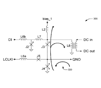
10022] FIG. 3A is a circuit schematic of an example RQL phase-mode
inverting D flip-
flop circuit 300 that can correspond to either of flip-flops 100 or 200. Flip-
flop 300 has two
logical inputs DI, LCLKI and one output QNO, each configured to receive or
transmit SFQ
pulses as inputs or outputs. A data signal consisting of positive and negative
SFQ pulses can be
provided on data input DI via data input inductor L6b, while a logical clock
signal consisting of
reciprocal SFQ pulse pairs can be provided on logical clock input LCLKI via
logical clock input
inductor L6a.
[0023] An AC and DC bias, labeled bias_1, can be provided to the circuit
via AC and DC
bias inductor L2. A DC bias can also be applied via a transformer coupling
grounded
inductor L8. As an example, AC and DC bias bias_l can provide (1:00/2 worth of
direct current
plus an AC waveform signal (e.g., a sinusoidal signal), while the DC bias
provided through
inductor L8 can provide 00/2 worth of direct current. As used herein, 430 is
one single flux
quantum, equal to approximately 2.07 mA-pH. When a reciprocal pulse pair is
applied at logical
clock input LCLKI, the output QNO takes on the inverted value of the data
input signal most
recently applied at data input DI. Rip-flop 300 can include four Josephson
junctions J2, J3, J4,
J5, and five inductors L2, L6a, L6b, L7, L8, the latter of which is a
transformer-coupled
7
CA 03118868 2021-05-05
WO 2020/112294 PCT/US2019/058797
inductor. Alternate examples, described herein, can include one fewer inductor
(eliminating
inductor L8) and/or can eliminate one Josephson junction by including a
resistor.
[0024] Inverting D flip-flop 300 is a "phase-mode" flip-flop inasmuch as
the logic value
of flip-flop 300 is stored as the superconducting phase of output Josephson
junction J4, either 0
or 27t radians, where Josephson junction superconducting phase is defined as
the time integral of
voltage at every node. In accordance with flip-flop 300 being a "phase-mode"
flip-flop, for any
single reciprocal pulse pair provided to logical clock LCLKI, at most only a
single pulse will be
observed at inverting output QNO. To improve the operating margins of circuit
300, data input
Josephson junction J2, along with data input inductor L6b and inductor L7,
provides some
isolation between the JTL (not shown) driving the data input DI and the
remainder of circuit 300
(as illustrated) that performs the logic operation. As such, in some examples,
data input inductor
L6bdata input Josephson junction J2, and inductor L7 can be considered as not
a part of
circuit 300 but rather as a part of the aforementioned data input driving JTL.
D flip-flop 300 is
therefore highly efficient in terms of its use of devices, requiring only
three or four Josephson
junctions and only three to five inductors, apart from any devices used for
race condition
avoidance phasing of input signals, and notably without requiring a separate
dedicated signal
inversion circuit stage.
[0025] As discussed below with regard to FIGS. 4 and 6, the DC
transformer and its
associated grounded inductor L8 can be omitted in some implementations,
provided that the DC
and AC mix provided by DC and AC bias bias_l can be appropriately adjusted.
Typical RQL
circuits are designed with DC and AC bias lines that provide a certain DC and
AC bias mix via
transformer coupling to a grounded bias inductor, and because flip-flop 300
uses a different mix
than ordinarily found in RQL circuits, DC bias transformer including inductor
L8 can be
advantageously included to provide a different mix while still making use of
the more readily
available bias from DC and AC bias source bias_1.
[0026] Although a more detailed description of the circuit's functioning
is given below, a
summary of the functioning of inverting flip-flop 300 is as follows. As can be
seen, for example,
in FIGS. 3L-3Q, the triggering of stacked Josephson junction J3 in flip-flop
300 drives one (Do
8
CA 03118868 2021-05-05
WO 2020/112294 PCT/US2019/058797
worth of current in all directions, including up into the two bias networks,
i.e., through
inductors L2 and L8, and the return path for this current is up from ground
through output
Josephson junction J4. Thus, for example, if DC and AC bias bias_l and DC bias
inductor L8
together provide 00/2 of positive DC bias current flowing down into circuit
300 through
inductor L2 and Josephson junctions J3 and J4 to ground at the bottom of the
circuit, the
triggering of Josephson junction J3, putting 4:00 of current flowing in the
opposite direction
reverses that whole loop, such that ¨00/2 worth of bias current is seen by
output Josephson
junction J4.
[00271 Escape Josephson junction J5 and output Josephson junction J4 in
circuit 300
together form a comparator, and depending on the direction of the DC bias
through output
Josephson junction J4, when a reciprocal pulse pair is introduced on logical
clock input LCLKI.
escape Josephson junction J5 either rejects the positive one of the logical
clock pulses and allows
the negative pulse to be passed through to the output QNO, or vice versa, with
the caveat that the
pulse is only passed to the output QNO provided that the output QNO is not
already in the state
implied by such pulse. In the case that the output QNO is already in the state
that would be
suggested by the passed pulse, escape Josephson junction J5 rejects both
pulses of the logical
clock reciprocal pulse pair. Because Josephson junction J3 is stacked with
output Josephson
junction J4 and triggers to reverse the bias current seen by output Josephson
junction J4, the data
input DI effectively applies an opposite bias to output Josephson junction J4,
such that a positive
pulse applied to data input DI triggers stacked Josephson junction J3
positively, and biases
output Josephson junction J4 negatively. Thus, a positive input at DI allows a
negative pulse to
transition from logical clock input LCLKI to output QNO.
[0028] The default state of circuit 300 with respect to the DC biases
provided from
bias_l and transformer-coupled inductor L8, as shown in FIG. 3A, is such that
DC bias currents
are provided in the positive direction, flowing from source bias_l down
through inductor L2,
stacked Josephson junction J3, and output Josephson junction J4. In the
circuit's default state
shown in FIG. 3A and prior to a circuit initialization described below,
circuit 300 is in "phase
9
CA 03118868 2021-05-05
WO 2020/112294 PCT/US2019/058797
mode zero": as shown in FIG. 3A, all of the Josephson junctions attached to
output QNO (J3, J4,
J5) have no dot on the output side, and the phase of the output QNO is at 0
radians.
[0029] FIGS. 3B-3R illustrate the functioning of circuit 300 starting
from the default
biasing state of FIG. 3A. In these illustrations, a dot placed next to a
Josephson junction
indicates that that Josephson junction has been triggered, and the side on
which said dot is placed
indicates the direction of triggering. In the convention used in these
illustrations, dots placed at
both sides of a Josephson junction indicate successive triggering and
untriggering of the
Josephson junction (i.e., triggering in one direction followed by triggering
in the opposite
direction), which is equivalent to no dots.
[0030] Operation of flip-flop circuit 300 can include an initial
reciprocal pulse pair at
logical clock input LCLKI to initialize the circuit. This initializing pulse
pair can consist, for
example, of a positive SFQ pulse followed by a negative SFQ pulse, as
illustrated in
FIGS. 3B-3E, but the circuit functions equivalently if the pulse pair consists
of a negative SFQ
pulse followed by a positive SFQ pulse. In FIG. 3B, a positive SFQ pulse 302
is applied to the
logical clock input LCLKI. This positive clock pulse triggers output Josephson
junction J4
positively and also negatively triggers stacked Josephson junction J3, as
indicated by the dots
next to those junctions in FIG. 3C. The triggering sends a positive output
pulse 304, shown in
FIG. 3C, to output QNO, thereby asserting the output and initializing it to a
logical "high" state,
which can correspond, for example, to a logical "1" in a larger digital logic
device or scheme,
such as a memory.
[0031] The negative triggering of stacked Josephson junction J3 means
that the triggering
of Josephson junction J4 does not reverse the bias in the ground-to-bias-
network loop as would
be the case in most other RQL circuits. In a typical RQL circuit, a single
biased Josephson
junction would go to a coupled transformer that applied DC and AC and would
eventually reach
ground, and that would form an inductive loop; a triggering of the single
Josephson junction
would drive one to worth of current up into that loop, reversing the biasing
seen by the single
Josephson junction from +00/2 to ¨00/2. In the case of circuit 300, the
presence of two
Josephson junctions in the biasing loop, J3 and J4, and the triggering of J3
upon the triggering of
CA 03118868 2021-05-05
WO 2020/112294 PCT/US2019/058797
J4, means that the current is not reversed in the loop. Thus, in flip-flop
300, the DC bias seen by
output Josephson junction J4 is not reversed at this point, i.e., in FIG. 3C,
because stacked
Josephson junction J3 has also been triggered, and from the perspective of the
ground-to-bias-
network loop, the triggering of both of these Josephson junctions cancels out
what would
otherwise be a bias-reversing effect. Plotted in terms of phase, the node
between Josephson
junctions J3 and J4 is at 2it radians while both of the nodes on the opposite
sides of these
Josephson junctions is at 0 radians.
[0032] In FIG. 3D, the negative SFQ pulse 306 of the logical clock
reciprocal pulse pair
is applied at logical clock input LCLKI. Because the DC bias of output
Josephson junction J4 is
still positive, inhibiting a negative triggering at output Josephson junction
J4, negative pulse 306
is unable to trigger output Josephson junction J4, and instead triggers escape
Josephson
junction J5 negatively, as shown in FIG. 3E by the dot to the right of escape
Josephson
junction 15. Consequently, the introduction of negative pulse 306 causes no
change in the
output. Thus, as shown in FIG. 3E, no pulse is propagated out of output QNO.
In other words,
FIG. 3E shows that negative logical clock pulse 306 has been rejected by the
triggering of escape
Josephson junction J5. From both of the initializing pulses 302, 306 provided
to logical clock
input LCKLI, only one pulse 304 has been propagated out of output QNO. The
initialization
being complete with the provision of both pulses of a first reciprocal pulse
pair at the logical
clock input LCLKI, circuit 3(X) is placed in "phase mode one": as shown in
FIG. 3E, all of the
Josephson junctions attached to output QNO (J3, J4, J5) have one dot on the
output side, and the
phase of the output QNO is at 27t radians.
[0033] With no input pulses applied at data input DI, any subsequent
logical clock
reciprocal pulse pairs arriving at logical clock input LCKLI will only trigger
escape Josephson
junction J5 and will have no effect on the output QNO, as shown in FIGS. 3F-
3I. Thus, for
example, FIG. 3F shows the arrival of the positive pulse 308 of a second or
subsequent logical
clock pulse pair at logical clock input LCLKI, in the absence of any input at
data input DL
FIG. 3G shows that this pulse 308 triggers escape Josephson junction J5 in the
opposite direction
(i.e., untriggers escape Josephson junction J5), as illustrated by dots on
both sides of escape
11
CA 03118868 2021-05-05
WO 2020/112294 PCT/US2019/058797
Josephson junction J5, which dots are both erased in the next drawing, FIG.
3H, consistent with
the notation convention that dots on both sides of a Josephson junction are
equivalent to no dots
at all.
[0034] In FIG. 3H, the negative pulse 310 of the second or subsequent
logical clock pulse
pair arrives at logical clock input LCLKI, still in the absence of any input
at data input DI.
FIG. 31 shows that this pulse 310 triggers escape Josephson junction J5
negatively, because the
DC bias of output Josephson junction J4 is still positive, such that negative
pulse 310 is unable to
trigger output Josephson junction J4. Thus, circuit 300 is in the same state
in FIG. 31 after
arrival of second or subsequent negative logical clock pulse 310 as it was in
FIG. 3E after the
arrival of first negative logical clock pulse 306. As long as the logical
clock continues to clock
with reciprocal pulse pairs with no data input to DI, circuit 300 sits in the
same phase mode
value and no output pulse is issued out of inverting output QNO.
[0035] FIG. 3J shows a positive SFQ pulse 312 being applied at data input
DI. As shown
in FIG. 3K, positive data input pulse 312 triggers input Josephson junction J2
positively,
propagating pulse 314, which in turn causes stacked Josephson junction J3 to
trigger positively,
as shown in FIG. 3L. As discussed previously, triggering stacked Josephson
junction J3 drives
one 41:00 worth of current into the two bias networks (i.e., up toward DC and
AC source bias_l
through inductor L2 and also toward L8 as well), thereby reversing the DC bias
seen by output
Josephson junction J4, because the return path for both of those loops is
through output
Josephson junction J4. In this way, the triggering of stacked Josephson
junction J3 ends up
negatively biasing output Josephson junction J4, thereby obtaining the
inversion effect of
circuit 300.
[0036] In this new bias state, when a reciprocal pulse pair is applied to
the logical clock
input LCLKI, as shown in FIGS. 3M-30, the positive logical clock pulse 316,
shown in
FIG. 3M, triggers escape Josephson junction J5, as shown by the additional dot
next to escape
Josephson junction J5 in FIG. 3N, and causes no change in the output QN0.
However, the
subsequent negative logical clock pulse 318, which is also shown in FIG. 3N,
triggers output
Josephson junction J4 negatively, as shown in FIG. 30, thus propagating
negative output
12
CA 03118868 2021-05-05
WO 2020/112294 PCT/US2019/058797
pulse 320, deasseiting the output QNO and resetting it to a logical "low"
state ("phase mode
zero"). This can correspond, for example, to a logical "0" in a larger digital
logic device or
scheme, such as a memory. Negative output pulse 320 in FIG. 30 corresponds to
positive data
input pulse 312 in FIG. 3J, as clocked in by negative logical clock input
pulse 318. The
conversion of the positive input pulse 312 into the negative output pulse 320
demonstrates the
inverting functionality of flip-flop circuit 300. This inversion is achieved
without the
requirement of passing any pulse through an inverter circuit stage.
[0037] It may be noted that FIG. 30 includes a dot over stacked Josephson
junction J3,
indicating a phase change of that Josephson junction as compared to FIG. 3N.
Every time output
Josephson junction J4 triggers, stacked Josephson junction J3 also triggers in
the opposite
direction, which is why the DC bias does not reverse. When output Josephson
junction J4
previously triggered positively (i.e., as the result of pulse 302), output
Josephson junction J4
received a dot on top (as seen in FIG. 3C) while stacked Josephson junction J3
triggered
negatively at the same time and received a dot on the bottom (also as seen in
FIG. 3C). Here, in
FIG. 30, when output Josephson junction J4 triggers negatively to receive a
dot on the bottom
(effectively canceling out the previous dot on top of output Josephson
junction J4), stacked
Josephson junction J3 triggers positively, thus receiving a dot on top.
[0038] FIGS. 3P and 3Q illustrate how a subsequent negative data input
pulse 322
applied at data input DI can negatively trigger input Josephson junction J2
and, subsequently,
stacked Josephson junction 33. This undoes the effects of the positive pulse
312 on data input DI
and, as shown in FIG. 3R, returns the DC biases seen by output Josephson
junction J4 to the
initial state, i.e., the same state shown in FIG. 3A, wherein output Josephson
junction J4 is biased
positively with bias current flowing down from the bias networks at the top
and right of
circuit 300 to the ground at the bottom. The next received logical clock pulse
pair will therefore
restore the circuit to "phase mode one" in the same manner as shown in FIGS.
3B-3E, outputting
a positive SFQ pulse, like pulse 304 in FIG. 3C, corresponding to negative
data input pulse 322
shown in FIG. 3P.
13
CA 03118868 2021-05-05
WO 2020/112294 PCT/US2019/058797
[0039] If, after introducing a positive pulse 312 to data input DI to
produce negative
output pulse 320 (as shown in FIGS. 3J-30), further clocking of the circuit is
done by provision
of additional reciprocal pulse pairs to logical clock input LCLKI in the
absence of pulses to data
input DL no phase mode change to circuit 300 will be obtained and no pulses
will issue from
output QNO. The only product of such additional clocking will be additional
triggering and
untriggering of escape Josephson junction J5 (similar to, but the inverse of,
the behavior
illustrated in FIGS. 3F-3I). After circuit initialization, output Josephson
junction J4 will only
trigger when the circuit is directed to put a new state to the output by
provision of an appropriate
pulse to data input DI.
[0040] Inverting flip-flop 300 uses reciprocal pulse pairs at logical
clock input to fully
evaluate its data inputs into its outputs. When the data input changes, on the
next logical clock
pulse pair, one or the other logical clock pulse will be allowed through to
the output, depending
on which logical state change is demanded by the circuit's previous logical
state and the data
input. In contrast to the functioning of many other RZ-data-encoded RQL
circuits, the two
logical clock pulses of a pulse pair are not required to both come within one
AC cycle of the
biasing network bias_1, but generally speaking, having both pulses of a
reciprocal pair come
within one AC cycle is advantageous, because separating them further in time
would only make
circuit 300 operate more slowly. The data input can advantageously be provided
at DI so as not
to change between the two pulses of any one logical clock reciprocal pulse
pair, because, in
effect, both pulses of a pulse pair supplied to logical clock input LCLKI
sample the data value
supplied at data input DI. Relative timing of data and logical clock pulses
can be enforced by
logic outside of the inverting flip-flop 300, i.e., elsewhere in the system of
which flip-flop 300 is
a part.
[0041] FIG. 4 is a circuit schematic of another example implementation
400 of an RQL
PML inverting D flip-flop circuit, similar in structure to circuit 300, but
with the elimination of
transformer-coupled grounded inductor L8. RQL biasing is usually implemented
via transformer
coupling to a grounded inductor. Therefore, by reducing the size of bias
inductor L2REDUCED in
circuit 4(X) as compared to inductor L2 in circuit 300 and reducing the AC
component of DC and
14
CA 03118868 2021-05-05
WO 2020/112294 PCT/US2019/058797
AC bias bias_l_ac_reduced in circuit 400 as compared to the AC component of DC
and AC bias
bias_l in circuit 300, this DC and AC bias source can effectively be combined
in parallel with
the DC bias source that would otherwise be supplied by now-eliminated grounded
inductor L8,
resulting in a smaller circuit. In the DC and AC bias source labeled in bias_l
in circuit 300,
there is additional inductance LSOuRCE (not shown in the drawings) that is
part of the
transformers that inject direct and alternating current. This additional
inductance LSOURCE is an
inductance to ground. Inductor L8 to be eliminated is also an inductance to
ground. Thus, the
size of L2REDUCED is set by the formula L8II(L2 + LsouacE) = 1,2REDUC.ED
',SOURCE, or,
equivalently, L2REDUCED = L8I1L2 + L8I1LsouRcE ¨ LsouRcE. In circuit 400 as
compared to
circuit 300, so that DC and AC bias source bias_l can provide 00/2 DC and
reduced-
amplitude AC. the amount of AC power coupled in the AC transformer (not shown)
associated
with bias_l_ac_reduced is modified so that the total AC bias level provided to
Josephson
junctions J3 and J4 is still the same in circuit 400 as in circuit 300. The
operation of circuit 400
is otherwise the same as previously described for circuit 300. D flip-flop 400
is therefore
extremely efficient in terms of its use of devices, requiring only three or
four Josephson junctions
and only two to four inductors, apart from any devices used for race condition
avoidance phasing
of input signals, and notably without requiring a separate dedicated signal
inversion circuit stage.
[0042] FIG. 5 is a circuit schematic of another example implementation
500 of an RQL
PML inverting D flip-flop circuit, similar in structure to circuit 300, but
with the substitution of
resistor R1 for escape Josephson junction J5. In circuit 300, operating
margins are significantly
more affected by variations in the size of escape Josephson junction J5 than
by variation in sizes
of other components in the circuit. In circuit 500, therefore, escape
Josephson junction J5 is
replaced by a small passive resistor Rl. The operation of circuit 500 is
substantially the same as
previously described for circuit 300, except as follows. In circuit 300, a
logical clock input pulse
that fails to trigger output Josephson junction J4 is dissipated by triggering
escape Josephson
junction J5, as shown, for example, in FIGS. 3E, 3G, and 31 (corresponding to
dissipated
pulses 306. 308, and 310, respectively). By contrast, in circuit 500, any such
pulse is dissipated
gradually in resistor R1 (e.g., into heat). Resistor R1 can be sized such that
the UR time
CA 03118868 2021-05-05
WO 2020/112294 PCT/US2019/058797
constant of the loop comprising logical clock input inductor L6a, dissipation
resistor R1, output
Josephson junction J4, and a logical clock input driving Josephson junction
(not shown, but
located between LCLIU and ground in FIG. 5) allows the loop to dissipate one
(1)0 worth of
current in less than one half of an AC cycle period as supplied by DC and AC
bias bias_1, such
that the pulse being dissipated does not interfere with the arrival of the
next logical clock pulse.
For example, the value of resistor R1 can be between about one ohm and about
ten ohms, e.g.,
between about two ohms and about five ohms. As with circuit 300, in circuit
500, AC and DC
bias source bias_l can provide c130/2 worth of direct current plus an AC
waveform signal (e.g., a
sinusoidal signal), while the DC bias provided through inductor L8 can provide
00/2 worth of
direct current. D flip-flop 500 is therefore highly efficient in terms of its
use of devices,
requiring only two or three Josephson junctions, one resistor, and only three
to five inductors,
apart from any devices used for race condition avoidance phasing of input
signals, and notably
without requiring a separate dedicated signal inversion circuit stage.
[0043] FIG. 6 is a circuit schematic of another example implementation
600 of an RQL
PML inverting D flip-flop circuit, similar in structure to circuit 300, but
with both the
elimination of transformer-coupled grounded inductor L8, as in circuit 400,
and the substitution
of resistor R1 for escape Josephson junction J5, as in circuit 500.
Accordingly, the size of bias
inductor L2 is reduced in circuit 600 as compared to circuit 300 and the AC
component of AC
and DC bias bias_l is reduced in circuit 600 as compared to circuit 300, as
described above with
regard to circuit 400. The operation of circuit 600 is otherwise the same as
previously described
for circuit 300. D flip-flop 600 is therefore extremely efficient in terms of
its use of devices,
requiring only two or three Josephson junctions, one resistor, and only two to
four inductors,
apart from any devices used for race condition avoidance phasing of input
signals, and notably
without requiring a separate dedicated signal inversion circuit stage.
[0044] FIG. 7A is a flow chart illustrating a method 700 of operating
(e.g., writing and
reading a logical value to and from) an inverting RQL phase-mode D flip-flop.
The flip-flop can
be like those described with reference to FIGS. 1, 2, 3A, 4, 5, or 6. An
inverting RQL flip-flop is
initialized 702 with logical clock reciprocal pulse pair to set the flip-flop
(i.e., its output) to a
16
CA 03118868 2021-05-05
WO 2020/112294 PCT/US2019/058797
phase mode corresponding to a logical "1" value. A positive SFQ pulse is then
provided 704 to a
data input of the inverting RQL flip-flop. A stacked Josephson junction in the
flip-flop is
triggered 706 to reverse the direction of a DC bias current flowing through an
output Josephson
junction in the flip-flop. Another reciprocal SFQ pulse pair is then provided
708 to a logical
clock input of the flip-flop. Only the negative pulse of the logical clock
pulse pair is passed 710
to the flip-flop output, based on reversed DC bias. The positive pulse of the
logical clock pulse
pair is absorbed 710 using either an escape Josephson junction or resistor to
absorb that pulse.
Thus, the flip-flop is reset 712 to a phase mode corresponding to a logical
"0" value. This
method can correspond, for example, to the functioning shown in FIGS. 3B-3E
and 3J-30.
[0045] FIG. 7B is a flow chart illustrating a method 714 of operating
(e.g., writing and
reading a logical value to and from) an inverting RQL phase-mode D flip-flop,
that can continue
from the method 700 of FIG. 7A. A negative SFQ pulse can be provided 716 to
the data input of
the inverting RQL flip-flop. This, in turn, untriggers 718 the stacked
Josephson junction in the
flip-flop to restore the (e.g., previously reversed) direction of the DC bias
current flowing
through the output Josephson junction in the flip-flop. Then, still another
reciprocal SFQ pulse
pair can be provided 720 to the logical clock input of the flip-flop. Now,
only the positive pulse
of the reciprocal pulse pair is passed 722 to the flip-flop output, based on
the restored DC bias,
while the negative pulse of the pulse pair is absorbed 722 with either an
escape Josephson
junction or a resistor. The flip-flop is thereby set 724 to a phase mode
corresponding to a
logical "1" value. This method can correspond, for example, to the functioning
shown in
FIGS. 3P-3R and 3B-3E.
[0046] The present disclosure provides a flip-flop with an inverted
output that improves
design efficiency by reducing the need for discrete inverters. The inverting
flip-flop described
herein is both smaller (in terms of part count and chip area required for
implementation) and
faster (in terms of signal propagation time) than implementations that combine
a flip-flop and an
inverter. These efficiency improvements lead to smaller die area and a lower
cost per die.
[0047] What have been described above are examples of the invention. It
is, of course,
not possible to describe every conceivable combination of components or
methodologies for
17
CA 03118868 2021-05-05
WO 2020/112294 PCT/US2019/058797
purposes of describing the invention, but one of ordinary skill in the art
will recognize that many
further combinations and permutations of the invention are possible.
Accordingly, the invention
is intended to embrace all such alterations, modifications, and variations
that fall within the
scope of this application, including the appended claims. Additionally, where
the disclosure or
claims recite "a," "an," "a first," or "another" element, or the equivalent
thereof, it should be
interpreted to include one or more than one such element, neither requiring
nor excluding two or
more such elements. As used herein, the term "includes" means includes but not
limited to, and
the term "including" means including but not limited to. The term "based on"
means based at
least in part on.
18