Note: Descriptions are shown in the official language in which they were submitted.
CA 03119305 2021-05-07
SECONDARY BATTERY AND MANUFACTURING METHOD
DESCRIPTION
Technical Field
[0001]
The present disclosure relates to a technique for improving the
performance of a secondary battery
Background Art
[0002]
Patent Literature 1 discloses a power storage element provided
with a power storage layer including a mixture of an insulating
material and n-type semiconductor particles between a first electrode
and a second electrode. A p-type semiconductor layer is disposed
between the power storage layer and the second electrode. Further, a
leak suppression layer is disposed between the p-type semiconductor
layer and the power storage layer. The leakage suppression layer is
composed of at least one element selected from silicon dioxide,
aluminum oxide, and magnesium oxide.
[0003]
Patent Literature 2 discloses a power storage element provided
with a power storage layer including a mixture of an insulating
material and n-type semiconductor particles between a first electrode
and a second electrode. A p-type semiconductor layer is disposed
between the power storage layer and the second electrode. Further, a
diffusion suppression layer having a resistivity of 1000 u.S2=cm or less
is disposed between the first electrode and the power storage layer.
The diffusion suppression layer is formed of nitride, carbide, and
boride.
Citation List
Patent Literature
[0004]
Patent Literature 1: Japanese Unexamined Patent Application
Publication No. 2016-82125
Patent Literature 2: Japanese Unexamined Patent Application
Date Re9ue/Date Received 2021-05-07
CA 03119305 2021-05-07
2
Publication No. 2016-91931
Summary of Invention
Technical Problem
[0005]
In such a secondary battery, further improvement in the
performance is desired.
[0006]
An object of the present disclosure is to improve the
performance of a secondary battery.
Solution to Problem
[0007]
An example aspect of an embodiment is a secondary battery
including: a first electrode; a second electrode; a first layer disposed
between the first electrode and the second electrode and including a
first n-type oxide semiconductor material; a second layer disposed on
the first layer and including a second n-type oxide semiconductor
material and a first insulating material; a third layer disposed on the
second layer and including tantalum oxide; and a fourth layer disposed
on the third layer and including a second insulating material.
[0008]
In the above secondary battery, the third layer may be an
amorphous layer including tantalum oxide or a nanoparticle layer
including a plurality of tantalum oxide nanoparticles.
[0009]
In the above secondary battery, a thickness of the third layer
may be 50 nm or more and 800 nm or less.
[0010]
In the above secondary battery, a layer including nickel oxide
or nickel hydroxide may be formed between the fourth layer and the
second electrode.
[0011]
In the above secondary battery, the fourth layer may be mainly
composed of SiOx that is the second insulating material, and metal
oxide may be added to the fourth layer.
Date Re9ue/Date Received 2021-05-07
CA 03119305 2021-05-07
3
[0012]
In the above secondary battery, the metal oxide may be SnOx.
[0013]
In the above secondary battery, the first insulating material may
be SiOx, and the second n-type oxide semiconductor material may be
TiO2.
[0014]
In the above secondary battery, the first n-type oxide
semiconductor material may be TiO2.
Another example aspect of the embodiment is a method of
manufacturing a secondary battery including: forming a first layer
including a first n-type oxide semiconductor material on a first
electrode; forming a second layer including a second n-type oxide
semiconductor material and a first insulating material on the first
layer; forming a third layer including tantalum oxide on the second
layer; forming a fourth layer including a second insulating material on
the third layer; and forming a second electrode on the fourth layer.
[0015]
In the above method, in the forming of the third layer, an
amorphous layer including tantalum oxide or a nanoparticle layer
including a plurality of tantalum oxide nanoparticles may be formed by
sputter deposition, vapor deposition, or ion plating.
Advantageous Effects of Invention
[0016]
According to the present disclosure, it is possible to provide a
technique of improving the performance of a secondary battery.
Brief Description of Drawings
[0017]
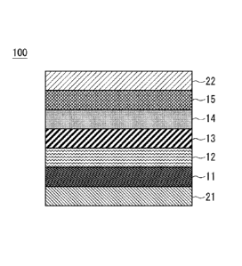
Fig. 1 schematically shows a laminated structure of a secondary
battery according to the first embodiment;
Fig. 2 is a graph showing a remaining rate of energy density
after one week in the secondary battery according to the first
embodiment;
Fig. 3 shows a surface SEM photograph of a tantalum oxide
Date Re9ue/Date Received 2021-05-07
CA 03119305 2021-05-07
4
film;
Fig. 4 shows an X-ray diffraction pattern in a sample with a
tantalum oxide film formed on a surface;
Fig. 5 is a flowchart showing a method of manufacturing the
secondary battery according to the first embodiment; and
Fig. 6 schematically shows a laminated structure of a secondary
battery according to a second embodiment.
Description of Embodiments
[0018]
An example of embodiments of the present disclosure will be
described below with reference to the drawings. The following
description shows preferred embodiments of the present disclosure, and
the technical scope of the present disclosure is not limited to the
following embodiments.
[0019]
[First embodiment]
(Laminated structure of secondary battery)
A basic configuration of a secondary battery according to this
embodiment will be described below with reference to Fig. 1. Fig. 1 is
a cross-sectional view schematically showing a laminated structure of
the secondary battery 100.
[0020]
In Fig. 1, the secondary battery 100 has a laminated structure in
which a first electrode 21, a first layer 11, a second layer 12, a third
layer 13, a fourth layer 14, a fifth layer 15, and a second electrode 22
are laminated in this order.
[0021]
[First electrode 21]
The first electrode 21 becomes a negative electrode of the
secondary battery 100. The first electrode 21 is a conductive sheet or
a conductive substrate functioning as a base material. As the first
electrode 21, for example, a metal foil sheet such as a SUS sheet or an
aluminum sheet can be used. Note that it is also possible to prepare a
base material formed of an insulator and form the first electrode 21 on
Date Re9ue/Date Received 2021-05-07
CA 03119305 2021-05-07
the substrate. When the first electrode 21 is formed on an insulating
base material, a metal material such as tungsten (W), chromium (Cr),
or titanium (Ti) can be used as the material of the first electrode 21.
As the material of the first electrode 21, an alloy film including
5 aluminum (Al), silver (Ag) or the like may be used. When the first
electrode 21 is formed on the base material, the first electrode 21 can
be formed in the same manner as the second electrode 22 described
later.
[0022]
[First layer 111
The first layer 11 is disposed on the first electrode 21. The
first layer 11 is disposed on the first electrode 21 on the side of the
second electrode 22. The first layer 11 is formed in contact with the
first electrode 21. The thickness of the first layer 11 is, for example,
about 50 nm to 200 nm.
[0023]
The first layer 11 includes an n-type oxide semiconductor
material (a first n-type oxide semiconductor material). The first layer
11 is an n-type oxide semiconductor layer formed with a predetermined
thickness. As the first layer 11, for example, titanium dioxide (TiO2),
tin oxide (S n02), or zinc oxide (ZnO) can be used. For example, the
first layer 11 is an n-type oxide semiconductor layer formed on the
first electrode 21 by sputtering, vapor deposition or the like. As the
material of the first layer 11, it is particularly preferable to use
titanium dioxide (TiO2).
[0024]
[Second layer 121
The second layer 12 functioning as a negative electrode active
material layer is disposed on the first layer 11. The second layer 12 is
disposed on the first layer 11 on the side of the second electrode 22.
The second layer 12 is formed in contact with the first layer 11. The
thickness of the second layer 12 is, for example, 200 nm to 1000 nm.
[0025]
The second layer 12 includes an insulating material (a first
Date Re9ue/Date Received 2021-05-07
CA 03119305 2021-05-07
6
insulating material). A silicone resin can be used as the first
insulating material. For example, as the first insulating material, it is
preferable to use a silicon compound (silicone) having a main
skeletone bonded by siloxane such as a silicon oxide. Therefore, the
second layer 12 includes silicon oxide (SiOx) as the first insulating
material.
[0026]
The second layer 12 includes an n-type oxide semiconductor
material (a first insulating material) in addition to an insulating
material (a second n-type oxide semiconductor material). That is, the
second layer 12 is formed of a mixture of the first insulating material
and the second n-type oxide semiconductor material. For example, a
fine particles n-type oxide semiconductor can be used as the second n-
type oxide semiconductor material.
[0027]
For example, the second layer 12 is formed of silicon oxide and
titanium dioxide with the second n-type oxide semiconductor material
used as titanium dioxide. In addition, as the n-type oxide
semiconductor material that can be used for the second layer 12, tin
oxide (Sn02), zinc oxide (Zn0), and magnesium oxide (MgO) are
preferable. A combination of two, three, or all of titanium dioxide, tin
oxide, zinc oxide, and magnesium oxide may also be used.
[0028]
The second n-type oxide semiconductor material included in the
second layer 12 and the first n-type oxide semiconductor material
included in the first layer 11 may be the same or different. For
example, when the first n-type oxide semiconductor material included
in the first layer 11 is titanium oxide, the second n-type oxide
semiconductor material of the second layer 12 may be titanium oxide
or an n-type oxide semiconductor material other than titanium oxide.
[0029]
[Third layer 13]
The third layer 13 functioning as a solid electrolyte is disposed
on the second layer 12. The third layer 13 is disposed on the second
Date Re9ue/Date Received 2021-05-07
CA 03119305 2021-05-07
7
layer 12 on the side of the second electrode 22. The third layer 13 is
formed in contact with the second layer 12. The thickness of the third
layer 13 is preferably 50 nm or more and 800 nm or less.
[0030]
The third layer 13 functions as a buffer layer for adjusting the
movement of H+ and electrons (c). The third layer 13 is a layer
including tantalum oxide. For example, the third layer 13 can be
formed of a tantalum oxide film (Ta0õ film) having a predetermined
thickness. Specifically, the third layer 13 is a Taft( layer formed on
the second layer 12 by sputtering or the like. The third layer 13 is
preferably an amorphous layer including tantalum oxide.
Alternatively, the third layer 13 is preferably a nanoparticle layer
including a plurality of tantalum oxide nanoparticles.
[0031]
[Fourth layer 14]
The fourth layer 14 functioning as a positive electrode active
material layer or a solid electrolyte layer is disposed on the third layer
13. The fourth layer 14 is disposed on the third layer 13 on the side of
the second electrode 22. The fourth layer 14 is formed in contact with
the third layer 13. The thickness of the fourth layer 14 is 100 nm to
150 nm. The fourth layer 14 may also be formed with a thickness in
the range of 50 nm to 250 nm. More desirably, the fourth layer 14 may
be formed with a thickness in the range from 150 nm to 200 nm.
[0032]
The fourth layer 14 functions as a buffer layer for adjusting the
movement of H + and electrons (er). The fourth layer 14 is a layer
including an insulating material (a second insulating material). The
fourth layer 14 includes silicon oxide (5i01) as the second insulating
material. Specifically, the fourth layer 14 is a layer mainly composed
of silicon oxide (SiOx) as the second insulating material.
[0033]
The fourth layer 14 may be composed of only the second
insulating material. Alternatively, in the fourth layer 14, a
conductivity adjusting material may be added to the second insulating
Date Re9ue/Date Received 2021-05-07
CA 03119305 2021-05-07
8
material. The mobility of H+ and e- can be further adjusted by adding
the conductivity adjusting material to the second insulating material.
That is, the fourth layer 14 may be a mixture layer in which the
conductivity adjusting material and an insulating material are mixed.
[0034]
The conductivity adjusting material may include an n-type oxide
semiconductor material (a third n-type oxide semiconductor material)
or oxide of metal. For example, the fourth layer 14 may include at
least one element selected from the group consisting of oxide of Ti,
Sn, Zn, Nb, or Mg as the conductivity adjusting material. By using
oxide of Sn, Zn, Ti, Nb, or Mg as the conductivity adjusting material,
the fourth layer 14 can be formed so as to be thick and be able to
withstand high electrical voltage.
[0035]
Specifically, tin oxide (SnOx) can be used as the third n-type
oxide semiconductor material included in the fourth layer 14. In this
case, the fourth layer 14 includes a mixture of silicon oxide and tin
oxide. In the fourth layer 14, the third n-type oxide semiconductor
material is added to silicon oxide, silicon nitride, or silicone oil. The
n-type oxide semiconductor is dispersed in silicon dioxide which is the
second insulating material.
[0036]
In the fourth layer 14, the third n-type oxide semiconductor
material may include one or more kinds of oxide selected from tin
(SnOx) oxide, zinc (ZnO) oxide, titanium oxide (TiOx), and niobium
(NbOx) oxide.
[0037]
The second n-type oxide semiconductor material included in the
second layer 12 and the third n-type oxide semiconductor material
contained in the fourth layer 14 may be the same material or different
materials. For example, if the third n-type oxide semiconductor
material in the fourth layer 14 is tin oxide, the second n-type oxide
semiconductor material of the second layer 12 may be tin oxide or an
n-type oxide semiconductor material other than tin oxide.
Date Re9ue/Date Received 2021-05-07
CA 03119305 2021-05-07
9
[0038]
[Fifth layer 15]
The fifth layer 15 is disposed on the fourth layer 14. The fifth
layer 15 is disposed on the fourth layer 14 on the side of the second
electrode 22. The fifth layer 15 is formed in contact with the fourth
layer 14. The thickness of the fifth layer 15 is 100 nm or more. The
fifth layer 15 may also be formed with a thickness within the range of
100 nm to 400 nm.
[0039]
The fifth layer 15 is formed on the fourth layer 14. The fifth
layer 15 includes a p-type oxide semiconductor material. The fifth
layer 15 is, for example, a nickel oxide (NiO) layer. The fifth layer 15
is formed on the fourth layer 14 by sputtering using Ni or NiO as a
target.
[0040]
[Second electrode 22]
The second electrode 22 is disposed on the fifth layer 15. The
second electrode 22 is formed in contact with the fifth layer 15. The
second electrode 22 may be formed of a conductive film. A metal
material such as chromium (Cr) or copper (Cu) may be used as the
material of the second electrode 22. An alloy film including aluminum
(Al), silver (Ag) or the like may also be used as the material of the
second electrode 22. Examples of the method of forming the alloy film
include the vapor phase film deposition method such as sputtering, ion
plating, electron beam vapor deposition, vacuum deposition, and
chemical vapor deposition. The metal electrode can be formed by
electrolytic plating, electroless plating or the like. As the metal used
for plating, copper, a copper alloy, nickel, silver, gold, zinc, tin or the
like can be commonly used. For example, the second electrode 22 is
an Al film having a thickness of 300 nm.
[0041]
In this manner, the third layer 13 including tantalum oxide is
disposed between the second layer 12 and the fourth layer 14. With
this configuration, the performance of the secondary battery 100 can be
Date Re9ue/Date Received 2021-05-07
CA 03119305 2021-05-07
improved. The performance of the secondary battery improved by this
configuration is described below using measurement data measured on
an actual sample.
[0042]
5 Fig. 2 is a graph showing the self-discharge characteristics of
the two samples A and B. The sample B is an example including the
third layer 13. The sample A is a comparative example not including
third layer 13. That is, in the sample A, the second layer 12 is
directly disposed on the fourth layer 14. Fig. 2 shows the results
10 measurement of the self-discharge characteristics one week after full
charge. That is, in Fig. 2, the remaining capacities after the secondary
batteries are left for one week are shown as the remaining rates (%),
provided that the remaining rate is 100% immediately after charging.
[0043]
The remaining rate of the sample B is higher than that of the
sample A. Therefore, the secondary battery according to this
embodiment including the third layer 13 can maintain a high remaining
rate. The reason for such a result is considered to be because
electrical resistances of an interface between the third layer 13 (the
solid electrolyte) and the second layer 12 (the negative electrode
active material) and an interface between the third layer 13 (the solid
electrolyte) and the fourth layer 12 (the positive electrode active
material) are increased, and thus the electron leakage can be prevented
or minimized. Therefore, according to this embodiment, it is possible
to prevent or minimize a rapid decrease in the energy density due to
the secondary battery being left after charging. According to the
configuration of this embodiment, for example, it is possible to
achieve the remaining rate of about 80% or more after the secondary
battery is left for six hours. Further, it is possible to achieve the
remaining rate of about 80% or more after 24 hours, and the remaining
rate of about 68% after 168 hours.
[0044]
Fig. 3 shows a surface SEM (Scanning Electron Microscope)
photograph of the third layer 13. Fig. 4 shows an X-ray diffraction
Date Re9ue/Date Received 2021-05-07
CA 03119305 2021-05-07
11
pattern (spectrum) with the third layer 13 exposed. In Fig. 4, the
horizontal axis represents a diffraction angle 20 (an angle between an
incident X-ray direction and a diffracted x-ray direction), and the
vertical axis represents a diffraction intensity (a.u). In this
embodiment, X-ray diffraction measurement is performed by the
grazing incidence X-ray diffraction method using CuKa rays each
having a wavelength of 1.5418 angstroms. Fig. 4 shows data of three
samples formed by changing the flow rate of an oxygen gas (02) to 0
sccm, 4 sccm, and 10 sccm at the time of sputter deposition. Figs. 3
and 4 show results of measurement when a Taft( film having a
thickness of 400 nm is formed as the third layer 13.
[0045]
As can be seen from the SEM photograph of Fig. 3, no particles
having a size of 0.1 gm or larger are formed in the third layer 13.
Furthermore, in Fig. 4, no diffraction peak appears. Therefore, it can
be seen that the Ta0x film is in an amorphous state or in a state where
a plurality of tantalum oxide nanoparticles are deposited. By forming
the Ta01 film having no crystal structure as the third layer 13, self-
discharge can be prevented or minimized. A high-performance
secondary battery can be realized.
[0046]
(Manufacturing process)
Next, a method of manufacturing the secondary battery 100
according to this embodiment will be described with reference to Fig.
5. Fig. 5 is a flowchart showing a method of manufacturing the
secondary battery 100.
[0047]
First, the first layer 11 is formed on the first electrode 21
(S11). The first layer 11 includes the first n-type oxide semiconductor
material as described above. For example, in the first layer 11, a TiO2
film can be formed as the first layer 11 by sputtering using Ti or TiO
as a target. The first layer 11 can be a TiO2 film having a thickness of
50 nm to 200 nm. The first electrode 21 is, for example, a tungsten
electrode.
Date Re9ue/Date Received 2021-05-07
CA 03119305 2021-05-07
12
[0048]
Next, the second layer 12 is formed on the first layer 11 (S12).
The second layer 12 can be formed by the coating pyrolysis process.
First, a coating liquid is prepared by mixing a solvent with a mixture
of a precursor of titanium oxide, tin oxide, or zinc oxide and silicone
oil. An example in which the second layer 12 is formed of silicon
oxide as the first insulating material and titanium oxide as the second
n-type oxide insulating material will be described. In this case, the
fatty acid titanium can be used as the precursor of the titanium oxide.
Fatty acid titanium and silicone oil are stirred together with a solvent
to prepare the coating liquid.
[0049]
The coating liquid is applied onto the first layer 11 by the spin
coating method, the slit coating method or the like. Specifically, the
coating liquid is applied by a spin coating apparatus at a rotational
speed of 500 to 3000 rpm.
[0050]
Then, the coating film is dried, baked, and irradiated with UV
light, so that the second layer 12 can be formed on the first layer 11.
For example, the workpiece is dried on a hot plate after the coating
liquid is applied. The drying temperature on the hot plate is about
C to 200 C, and the drying time is about 5 minutes to 30 minutes.
After the workpiece is dried, the workpiece is baked in the atmosphere
using a baking furnace. The baking temperature is, for example, about
25 300 C to 600 C, and the baking time is about 10 minutes to 60
minutes.
[0051]
Thus, an aliphatic acid salt is decomposed to form a fine
particle layer of titanium dioxide covered with a silicone insulating
30 film. Specifically, the fine particle layer has a structure in which a
metal salt of the titanium dioxide coated with silicone is buried in a
silicone layer. The baked coating film is irradiated with UV light by a
low-pressure mercury lamp. The UV irradiation time is 10 to 60
minutes.
Date Re9ue/Date Received 2021-05-07
CA 03119305 2021-05-07
13
[0052]
When the second n-type oxide semiconductor is titanium oxide,
for example, titanium stearate can be used as another example of the
precursor. Titanium oxide, tin oxide, and zinc oxide are formed by
decomposing an aliphatic acid salt which is a precursor of a metal
oxide. For titanium oxide, tin oxide, zinc oxide, and the like, it is
also possible to use fine particles of an oxide semiconductor without
using a precursor. Nanoparticles of titanium oxide or zinc oxide are
mixed with silicone oil to produce a mixture. Further, a solvent is
mixed with the mixture to produce the coating liquid.
[0053]
The third layer 13 is formed on the second layer 12 (S13). The
third layer 13 includes the tantalum oxide as described above. For
example, the third layer 13 can be formed by sputtering using Ta or
Ta205 as a target. Alternatively, instead of the sputter deposition, the
film formation method such as the vapor deposition or ion plating can
be used. The Ta0õ film can be formed as the third layer 13 by using
these film forming methods. In the sputter deposition, only an argon
(Ar) gas may be used, or an oxygen (02) gas may be added to the argon
gas and then supplied. The third layer 13 may be a Ta0x film having a
thickness of 50 nm or more and 800 nm or less. Here, as the third
layer 13, it is preferable to form an amorphous Ta0x film or a Taft(
film in which a plurality of tantalum oxide nanoparticles are deposited.
[0054]
The fourth layer 14 is formed on the third layer 13 (S14). The
fourth layer 14 can be formed in the same manner as the second layer
12. Specifically, fatty acid tin and silicone oil are stirred together
with a solvent to prepare a chemical solution. This chemical solution
is applied onto the third layer 13 using the spin coating apparatus.
The rotational speed is, for example, about 500 to 3000 rpm. After the
chemical solution is applied, the workpiece is dried on the hot plate.
The drying temperature on the hot plate is, for example, about 30 C to
200 C, and the drying time is, for example, about 5 to 30 minutes.
[0055]
Date Re9ue/Date Received 2021-05-07
CA 03119305 2021-05-07
14
After the workpiece is dried, the workpiece is baked. The
baking furnace is used to bake the workpiece after the workpiece is
dried, and the workpiece is baked in the atmosphere. The baking
temperature is, for example, about 300 C to 600 C, and the baking
time is, for example, about 10 to 60 minutes. After the workpiece is
baked, the workpiece is irradiated with UV light by the low-pressure
mercury lamp. The UV irradiation time is, for example, about 10 to
100 minutes. The thickness of the fourth layer 14 after the UV
irradiation is, for example, about 100 nm to 300 nm.
[0056]
For the tin oxide, it is also possible to use fine particles of an
oxide semiconductor without using a precursor. Tin oxide
nanoparticles are mixed with silicone oil to produce a mixture.
Further, a solvent is mixed with the mixture to produce the coating
liquid.
[0057]
Another example of the step of forming the fourth layer 14 will
be described. In this example, a layer made of only the second
insulating material is used as the fourth layer 14. That is, a method of
forming the fourth layer 14 not including the third n-type oxide
semiconductor material will be described below.
[0058]
The silicone oil is stirred together with a solvent to prepare a
chemical solution. This chemical solution is applied onto the third
layer 13 using the spin coating apparatus. Here, the spin coating
apparatus is used. The rotational speed of the spin coating apparatus
is, for example, about 500 to 3000 rpm. After the chemical solution is
applied, the workpiece is dried on the hot plate. The drying
temperature on the hot plate is, for example, about 50 C to 200 C,
and the drying time is, for example, about 5 to 30 minutes.
[0059]
After the workpiece is dried, the workpiece is baked. The
baking furnace is used to bake the workpiece after the workpiece is
dried, and the workpiece is baked in the atmosphere. The baking
Date Re9ue/Date Received 2021-05-07
CA 03119305 2021-05-07
temperature is, for example, about 300 C to 600 C, and the baking
time is, for example, about 10 to 60 minutes. After the workpiece is
baked, the workpiece is irradiated with UV light by the low-pressure
mercury lamp. The UV irradiation time is, for example, about 10 to 60
5 minutes. The thickness of the fourth layer 14 after the UV irradiation
is, for example, about 10 nm to 100 nm.
[0060]
Next, the fifth layer 15 is formed on the fourth layer 14 (S15).
The fifth layer 15 can be formed by sputtering using Ni or NiO as a
10 target.
[0061]
The second electrode 22 is formed on the fifth layer 15 (S16).
Examples of the method of forming the second electrode 22 include the
vapor phase film deposition method such as sputtering, ion plating,
15 electron beam vapor deposition, vacuum deposition, and chemical
vapor deposition. Note that the second electrode 22 may be partially
formed using a mask. The second electrode 22 can be formed by the
electrolytic plating method, the electroless plating method or the like.
As the metal used for the plating, copper, a copper alloy, nickel,
silver, gold, zinc, tin or the like can commonly be used. For example,
the second electrode 22 is an Al film having a thickness of 300 nm.
[0062]
With the above-described manufacturing method, the high-
performance secondary battery 100 can be manufactured with high
productivity.
[0063]
[Second embodiment]
A configuration of a secondary battery 100A according to a
second embodiment will be described with reference to Fig. 6. Fig. 6
is a cross-sectional view showing the configuration of the secondary
battery 100A. In this embodiment, a sixth layer 16 is provided in
place of the fifth layer 15. The secondary battery 100A has a
laminated structure in which the first electrode 21, the first layer 11,
the second layer 12, the third layer 13, the fourth layer 14, the sixth
Date Re9ue/Date Received 2021-05-07
CA 03119305 2021-05-07
16
layer 16, and the second electrode 22 are laminated in this order. The
structure other than the sixth layer 16 is the same as that of the first
embodiment, and thus the description of the secondary battery 100A
will be omitted as appropriate.
[0064]
The sixth layer 16 includes nickel hydroxide (Ni(OH)2).
Specifically, a nickel hydroxide layer formed with a predetermined
thickness becomes the sixth layer 16. The thickness of the sixth layer
16 is preferably 100 nm or more and 400 nm or less.
[0065]
As the method of forming the sixth layer 16, the chemical bath
deposition (CBD) method, the dip-coating method, or the mist CVD
method can be used. In the chemical bath deposition method or the
dip-coating method, a solution including nickel ions is used.
Specifically, an alkaline aqueous solution is reacted with an aqueous
solution including nickel ions to deposit a nickel hydroxide layer on
the surface of the fourth layer 14.
[0066]
In this way, the nickel hydroxide film is directly formed on the
fourth layer 14 by the chemical bath deposition method, the dip-
coating method or the like. Since the sixth layer 16 can be formed
with a sufficient thickness, a secondary battery having a large storage
capacity can be realized. That is, in the configuration in which nickel
oxide is electrically converted into nickel hydroxide, it is difficult to
obtain a sufficient storage capacity, because the film is thin.
[0067]
The secondary battery may include both the fifth layer 15 and
the sixth layer (the nickel hydroxide layer) 16. In this case, the sixth
layer 16 may be formed on the fifth layer 15, and the fifth layer 15
may be formed on the sixth layer 16. Further, two NiO layers may be
provided between the second electrode 22 and the fourth layer (SiOx +
SnOx) 14, and the nickel hydroxide layer may be provided between the
two NiO layers. A layer other than the above-described first layer 11
to the sixth layer 16 may be added.
Date Re9ue/Date Received 2021-05-07
17
[0068]
While examples of embodiments of the present disclosure have been
described above, the present disclosure includes appropriate modifications
that
do not impair objects and advantages of the present disclosure, and is not
limited
s by the embodiments described above.
Reference Signs List
[0070]
100 SECONDARY BATTERY
11 FIRST LAYER (n-TYPE OXIDE SEMICONDUCTOR LAYER)
12 SECOND LAYER (SiOx + TiOx)
13 THIRD LAYER (Ta0x)
14 FOURTH LAYER (SiOx + SnOx)
FIFTH LAYER (NICKEL OXIDE LAYER)
16 SIXTH LAYER (NICKEL HYDROXIDE LAYER)
15 21 FIRST ELECTRODE
22 SECOND ELECTRODE
Date Recue/Date Received 2022-11-28