Note: Descriptions are shown in the official language in which they were submitted.
WO 2020/097742 PCT/CA2019/051637
- 1 -
OPTICAL GYROSCOPES AND
METHODS OF MANUFACTURING OF OPTICAL GYROSCOPES
CROSS - REFERENCE
[0001] The present application claims priority to U.S. Patent Application No.
62/768,322,
filed on November 16, 2018, the entirety of which is incorporated herein by
reference.
TECHNICAL FIELD
[0002] The present technology generally relates to optical gyroscopes.
BACKGROUND
[0003] Fiber optics gyroscopes (FOGs) are known to be used for sensing changes
in a
device's orientation based on Sagnac effect. A typical FOG has a coil of
optical fiber
which can be as long as 5 km. Resonant micro-photonic gyroscopes (RMGs), on
the
other hand, may be 50 times smaller, 30 times cheaper, and more reliable than
FOGs.
Moreover, RMGs may consume eight times less energy than FOGs, for the same
performance.
[0004] Certain conventional RMGs are made using crystalline-based whispering
gallery
mode resonators (WGMR). The WGMR has a resonator and an input evanescent prism
coupler to couple the light in and out of the resonator. The WGMR is typically
made of
Calcium Fluoride (CaF2). Certain other RMGs are made using a micro-resonator
disk
and fabricated of silica. Light from an external cavity diode laser is coupled
to the disk
resonator using a tapered fiber.
[0005] The performance of the conventional RMGs, known in the art, is, in
part, limited
by a quality factor Q (so-called "Q-factor") of its resonator. Although the 0-
factor of
5.3x101 may be reached theoretically, fabrication constraints and limitations
often result
in an undesirable decrease of the overall 0-factor of the resonator of the
gyroscope.
WO 2020/097742 PCT/CA2019/051637
- 2 -
SUMMARY
[0006] An object of the present disclosure is to provide a gyroscope chip and
a method
of manufacturing of the gyroscope chip that improves the capabilities of
currently
existing RMGs, or reduces or overcomes disadvantages associated therewith. The
object of the present disclosure includes providing a gyroscope chip with an
integrated
coupling element. In particular, a ring resonator and a waveguide are
immovably
attached to a substrate. In the gyroscope chip with lateral coupling as
described herein,
both waveguide core and ring core have wedge shapes to reduce losses of the
electromagnetic mode. A gyroscope chip with vertical coupling as described
herein has
a ring core with a wedge shape. Due to the integrated implementation as
described
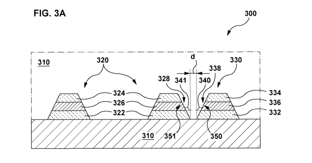
herein, in certain embodiments, the chip is robust to shocks and vibrations,
while
attaining high values of the 0-factor (e.g. higher than 100.106) and thus
allowing for a
low measurable angular velocity 60 (e.g. lower than 0.2 deg/h for a resonator
diameter
of 10 mm).
[0007] In accordance with this objective, an aspect of the present disclosure
provides a
chip for an optical gyroscope, the chip comprising: a substrate having an
upper surface;
a waveguide on the upper surface of the substrate, the waveguide comprising: a
first
waveguide cladding layer immovably attached to the substrate; and a waveguide
core
immovably attached to the first waveguide cladding layer; and a ring resonator
on the
upper surface of the substrate and spaced from the waveguide, the ring
resonator
comprising: a first ring cladding layer immovably attached to the substrate;
and a ring
resonator core immovably attached to the first ring cladding layer and having
a side
wall, the side wall of the ring resonator core forming an obtuse angle with
the upper
surface of the substrate. By a chip for an optical gyroscope it is meant at
least a portion
of an optical gyroscope. In certain embodiments, there is provided an optical
gyroscope
including the chip as described herein, and optionally including one or more
of a light
source, a detector, signal transducers, signal modulators.
[0008] In some embodiments, the waveguide core is located in the same plane as
the
ring resonator core. The waveguide may further comprise a second waveguide
cladding
WO 2020/097742 PCT/CA2019/051637
- 3 -
layer on the waveguide core, and the ring resonator further comprises a second
resonator cladding layer on the ring resonator core, the waveguide core being
located
between the first waveguide cladding layer and the second waveguide cladding
layer;
and the ring resonator core being located between the first resonator cladding
layer and
the second resonator cladding layer. A width of the waveguide core may be
larger than
a width of the second waveguide cladding layer. In certain embodiments, the
waveguide
core has a side wall which forms an obtuse angle to the upper surface of the
substrate.
In these embodiments, by width is meant an average width. In other embodiments
the
side wall is perpendicular to the upper face. In certain embodiments, the
refractive index
of the waveguide core is greater than a refractive index of the first
waveguide cladding
layer and the second waveguide cladding layer. In certain embodiments, the
refractive
index of the waveguide core is greater than a cladding at least partially
surrounding the
waveguide core.
[0009] A side wall of the waveguide may be smooth, so that a width of the
waveguide
smoothly reduces going from the second waveguide cladding layer to the
waveguide
core, and to the first waveguide cladding layer. By smooth is meant that the
side wall
has a continuous form. A cross-sectional profile of the side wall may be
straight or
curved. The second waveguide cladding layer and the second ring cladding layer
may
be made of silicon dioxide. A side wall of the ring resonator may be smooth,
so that a
width of the ring resonator smoothly reduces going from the second ring
cladding layer
to the waveguide core, and to the first ring cladding layer. By smooth is
meant that the
side wall has a continuous form. A cross-sectional profile of the side wall
may be
straight or curved.
[00010] In at least one embodiment, the waveguide may further comprise
a
second waveguide cladding layer that is immovably attached to and covers the
first
waveguide cladding layer and the waveguide core; the ring resonator core is
located in
a ring plane; the first ring cladding layer is immovably attached to the
second waveguide
cladding layer, and the waveguide core is located in a waveguide plane that is
parallel
to the disk plane such that the light transfers its energy from the waveguide
plane to the
ring plane.
WO 2020/097742 PCT/CA2019/051637
- 4 -
[00011] The first ring cladding layer may have a width that is less than a
width of
the ring resonator core. The first ring cladding layer may be narrower than
the ring
resonator core. In at least one embodiment, a side wall of the waveguide core
may form
an obtuse angle with the upper surface of the substrate. The waveguide core
may have
a wedge shape facing the ring resonator core. The obtuse angle may be between
about
100 degrees and about 170 degrees.
[00012] The chip may further comprise a coating layer immovably attached to
and
covering the ring resonator and the waveguide. In certain embodiments, in
which the
first waveguide cladding layer and the first ring cladding layer form a first
cladding layer,
the coating layer covers the first cladding layer. In at least one embodiment,
the first
waveguide cladding layer and the first ring cladding layer form a first
cladding layer; and
a coating layer is immovably attached to and covers the first cladding layer,
the ring
resonator core, and the waveguide core. The ring resonator core and the
waveguide
core may be made of silicon nitride. The coating layer may be made of silicon
dioxide.
[00013] The first waveguide cladding layer and the first ring cladding
layer may be
made by partially by isotopically etching the substrate using Xenon Fluoride
(XeF2) gas.
In certain embodiments, the first waveguide cladding layer is chemically
etched on the
upper face of the substrate, and the first ring cladding layer is chemically
etched on the
upper face of the substrate.
[00014] The substrate may be made of silicon. The first waveguide cladding
layer
and the first ring cladding layer may be made of silicon dioxide. The ring
resonator core
and the waveguide core may be made of silicon dioxide. The ring resonator core
may
be made of silicon dioxide and the waveguide core is made of silicon nitride.
The first
waveguide cladding layer and the first ring cladding layer may be made of a
thermal
dioxide.
[00015] In at least one embodiment, the substrate may have at least one of
a ring
groove formed in the upper surface of the substrate, and a waveguide groove
formed in
the upper surface of the substrate. The resonator and the waveguide may be
made of
portions of an optical fiber immovably attached to the substrate, the
waveguide core and
WO 2020/097742 PCT/CA2019/051637
- 5 -
the resonator core being a core of the optical fiber and the first waveguide
cladding
layer and the first ring cladding layer being a cladding of the optical fiber.
[00016] The chip may further comprise a fiber groove formed in the upper
surface
of the substrate and adapted to receive a portion of a coupling optical fiber
for delivering
a light from coupling optical fiber to the waveguide.
[00017] From another aspect, there is provided a chip for an optical
gyroscope, the
chip comprising: a substrate having an upper surface; a waveguide on the upper
surface of the substrate, the waveguide comprising: a first waveguide cladding
layer
immovably attached to the substrate; and a waveguide core immovably attached
to the
first waveguide cladding layer; and a ring resonator on the upper surface of
the
substrate and spaced from the waveguide, the ring resonator comprising: a
first ring
cladding layer immovably attached to the substrate; and a ring resonator core
immovably attached to the first ring cladding layer and having a side wall,
the side wall
of the ring resonator core forming an obtuse angle with the upper surface of
the
substrate, wherein the ring resonator and the waveguide are made of portions
of an
optical fiber immovably attached to the substrate, the waveguide core and the
resonator
core being a core of the optical fiber and the first waveguide cladding layer
and the first
ring cladding layer being a cladding of the optical fiber
[00018] In accordance with another aspect of the present disclosure, a
chip for an
optical gyroscope comprises: a substrate having a ring groove formed in an
upper face
of the substrate and a waveguide groove formed in the upper face of the
substrate and
spaced from the ring groove; an optical fiber ring made of one loop of an
optical fiber
located in the ring groove in the substrate; and an optical fiber waveguide
made of the
optical fiber located in waveguide groove in the substrate. The ring groove
and the
waveguide groove may be made by etching the substrate. The optical fiber ring
and the
optical fiber waveguide may be immovably attached to the substrate. At least a
portion
of the optical fiber waveguide may be tangentially oriented with respect to
the optical
fiber ring. The chip may further comprise a lid adapted to cover the
substrate, the ring
groove, the waveguide groove, the optical fiber ring and the optical fiber
waveguide.
WO 2020/097742 PCT/CA2019/051637
- 6 -
[00019] In accordance with another aspect of the present disclosure, a
method of
manufacturing a chip for an optical gyroscope is provided. The method
comprises
depositing a first cladding layer an upper surface of a substrate; depositing
a core layer
on the first cladding layer; depositing a resist mask pattern above the core
layer to
define: a form of a ring resonator core and a form of a waveguide core and
spaced
from the ring resonator core; etching the core layer outside of the resist
mask pattern to
form an obtuse angle of a side wall of the ring resonator core with the upper
surface of
the substrate; and stripping the resist mask pattern off. In certain
embodiments, the
substrate can be made of silicon. In certain embodiments, the waveguide core
is
positioned tangentially to the ring resonator and located at a gap distance
therefrom.
[00020] The method may further comprise: prior to depositing the resist
mask
pattern, depositing a second cladding layer on the core layer; depositing a
resist mask
pattern on the second cladding layer; and, in addition to etching the core
layer, etching
the second cladding layer outside of the resist mask pattern. The method may
further
comprise: in addition to etching the core layer, etching the first cladding
layer outside of
the resist mask pattern.
[00021] The method may further comprise: after stripping the resist
mask,
depositing a coating layer to cover the first cladding layer, the ring
resonator core, and
the waveguide core. The etching the core layer outside of the resist mask
pattern may
further comprise forming an obtuse angle between a side wall of the waveguide
core
and the upper surface of the substrate.
[00022] In accordance with another aspect of the present disclosure,
another
method of manufacturing a chip for an optical gyroscope comprises: depositing
a first
cladding layer on an upper surface of a substrate; depositing a core layer on
the first
cladding layer; depositing a resist mask pattern to define a form of a ring
resonator core;
etching the core layer outside of the resist mask pattern to form an obtuse
angle of a
side wall of the ring resonator core with the upper surface of the substrate;
stripping the
resist mask pattern off; depositing a waveguide core positioned tangentially
to the ring
resonator core and located at a gap distance from the ring resonator core. The
method
WO 2020/097742 PCT/CA2019/051637
- 7 -
may further comprise depositing a coating layer to cover the first cladding
layer, the ring
resonator core, and the waveguide core.
[00023] In accordance with another aspect of the present disclosure,
another
method of manufacturing a chip for an optical gyroscope comprises: depositing
a first
waveguide cladding layer on a silicon substrate; depositing a first waveguide
core layer
and etching the first waveguide core layer to obtain a waveguide core;
depositing a
second waveguide cladding layer to cover the waveguide core and the first
waveguide
cladding layer; depositing a ring supporting layer and etching it to obtain a
first ring
cladding layer; and depositing a ring resonator core layer and etching the
ring resonator
core layer to obtain a ring resonator core and to form an obtuse angle of a
side wall of
the ring resonator core with the upper surface of the substrate. The method
may further
comprise depositing a coating layer on the ring resonator core and the second
waveguide cladding layer.
[00024] In accordance with another aspect of the present disclosure,
another
method of manufacturing a chip for an optical gyroscope comprises: etching a
ring
groove in an upper surface of a substrate adapted to receive an optical fiber
ring, the
optical fiber ring having a circular form; etching a waveguide groove in the
upper
surface of the substrate adapted to receive an optical fiber waveguide,;
placing the
optical fiber ring into the ring groove; and placing the optical fiber
waveguide into the
waveguide groove. The etching the waveguide groove may further comprise
partially
overlapping the waveguide groove with the ring groove at least at a feeding
point, the
waveguide groove and the ring groove forming a common groove at least at the
feeding
point, portions of the optical fiber ring and the optical fiber waveguide
being located in
the common groove. The method may further comprise: splicing two ends of an
optical
fiber to form the optical fiber ring, the two ends forming a ring junction;
and annealing
the ring junction of the optical fiber ring prior to placing the optical fiber
ring into the ring
groove. The method may further comprise immovably attaching the optical fiber
waveguide to the waveguide groove and immovably attaching the optical fiber
ring to
the ring groove.
WO 2020/097742 PCT/CA2019/051637
- 8 -
[00025] .. Implementations of the present disclosure each have at least one of
the
above-mentioned object and/or aspects, but do not necessarily have all of
them. It
should be understood that some aspects of the present disclosure that have
resulted
from attempting to attain the above-mentioned object may not satisfy this
object and/or
may satisfy other objects not specifically recited herein.
[00026] Additional and/or alternative features, aspects and advantages of
implementations of the present disclosure will become apparent from the
following
description, the accompanying drawings and the appended claims.
BRIEF DESCRIPTION OF THE DRAWINGS
[00027] Further features and advantages of the present disclosure will
become apparent
from the following detailed description, taken in combination with the
appended drawings,
in which:
[00028] FIG. 1 depicts a conventional RMG 100;
[00029] FIG. 2 depicts a perspective view of a gyroscope chip, in
accordance with
various embodiments of the present disclosure;
[00030] FIG. 3A depicts a cross-sectional view of the gyroscope chip of
FIG. 2 taken
along a line A-A in FIG. 2;
[00031] FIG. 3B depicts a zoomed-in portion of the cross-sectional view of
the
gyroscope chip of FIG. 3A;
[00032] FIG. 4A depicts a cross-sectional view of the gyroscope chip of
FIG. 2 taken
along the line A-A in FIG. 3A, at one step of a plurality method steps of
manufacturing of
the gyroscope chip, in accordance with various embodiments of the present
disclosure;
[00033] .. FIG. 4B depicts a cross-sectional view of the gyroscope chip of
FIG. 3A taken
along the line A-A in FIG. 3, at another step of the plurality of method steps
of
manufacturing of the gyroscope chip, in accordance with various embodiments of
the
present disclosure;
WO 2020/097742 PCT/CA2019/051637
- 9 -
[00034] FIG. 5A depicts a cross-sectional view of an alternative embodiment
of the
gyroscope chip of FIG. 2 taken along the line A-A in FIG. 2, in accordance
with various
embodiments of the present disclosure;
[00035] FIG. 5B depicts a cross-sectional view of a portion of another
embodiment of
the gyroscope chip with a waveguide with an extended waveguide core, in
accordance
with various embodiments of the present disclosure;
[00036] FIG. 6 depicts cross-sectional views of another embodiment of the
gyroscope
chip of the present technology at various steps of a method of manufacturing
thereof, in
accordance with various embodiments of the present disclosure;
[00037] FIG. 7 depicts a perspective view of another embodiment of a
gyroscope chip,
in accordance with various embodiments of the present disclosure;
[00038] FIG. 8A depicts a cross-sectional view of a gyroscope chip with
vertical coupling
(GCVC), in accordance with various embodiments of the present disclosure;
[00039] FIG. 8B depicts a top view of the GCVC of FIG. 8A;
[00040] FIG. 9A depicts an intrinsic 0-factor and a coupling coefficient
simulated as
functions of a coupling length of the GCVC of FIG. 8A with a ring resonator
core made of a
silicon dioxide, and waveguide core made of a silicon nitride, in accordance
with various
embodiments of technology described herein;
[00041] FIG. 9B depicts a ring resonator transmission spectrum of the GCVC
of FIG.
9A;
[00042] FIG. 1 OA depicts the intrinsic 0-factor and the coupling
coefficient simulated as
functions of the coupling length of the GCVC of FIG. 8A, with a ring resonator
core made
of a silicon dioxide and waveguide core made of a silicon dioxide, in
accordance with
various embodiments of the present disclosure;
[00043] FIG. 10B depicts a ring resonator spectrum of the GCVC of FIG. 10A;
[00044] FIG. 11A depicts mode profiles in ring resonator core simulated for
the GCVC
having a ring resonator core made of a silicon dioxide and a waveguide core
made of a
silicon nitride, in accordance with various embodiments of the present
disclosure;
WO 2020/097742 PCT/CA2019/051637
- 10 -
[00045] FIG. 11B
depicts mode profiles in ring resonator core simulated for the GCVC
having the ring resonator core made of a silicon dioxide and the waveguide
core also
made of a silicon dioxide, in accordance with various embodiments of the
present
disclosure;
[00046] FIG. 11C
depicts mode profiles in ring resonator core simulated for GCVC
having the ring resonator core made of a silicon nitride and the waveguide
core also made
of a silicon nitride with air partially surrounding the ring resonator core,
in accordance with
various embodiments of the present disclosure;
[00047] FIG. 11D
depicts mode profiles in ring resonator core simulated for GCVC
having the ring resonator core made of a silicon nitride and the waveguide
core also made
of a silicon nitride with a coating layer partially surrounding the ring
resonator core, in
accordance with various embodiments of the present disclosure;
[00048] FIG. 12
depicts a perspective view of a portion of a fiber groove, in accordance
with various embodiments of the present disclosure; and
[00049] FIG. 13
depicts a top plan view of a fiber gyroscope chip, in accordance with
various embodiments of the present disclosure.
[00050] It is to be understood that throughout the appended drawings and
corresponding descriptions, like features are identified by like reference
characters.
Furthermore, it is also to be understood that the drawings and ensuing
descriptions are
intended for illustrative purposes only and that such disclosures do not
provide a
limitation on the scope of the claims.
DETAILED DESCRIPTION
[00051] The instant disclosure is directed to systems, methods and apparatuses
to
address the deficiencies of the current state of the art. To this end, the
instant disclosure
describes apparatuses, and methods of manufacturing thereof, directed to
increasing of a
0-factor of a gyroscope.
[00052] FIG. 1
depicts a conventional RMG 100 as it is known in the art. The
conventional RMG 100 has a conventional rotation sensing element 110 and a RMG
WO 2020/097742 PCT/CA2019/051637
- 11 -
waveguide 112. An external laser source 114 feeds a light beam 116 via an
optical
waveguide 118 to the RMG waveguide 112, which, in turn, delivers the light to
the
rotation sensing element 110. Changes in orientation of the conventional RMG
100 are
determined based on a difference between path delays of the light beam
travelling
clockwise (CW) and counter clockwise (CCW), measured by a photodetector 120.
[00053] A
value of RMG's minimum measurable angular velocity (so-called
"measurement uncertainty") Of) needs to be as small as possible in order to
improve the
precision of the measurement of any changes in the orientation of the RMG. The
RMG's
minimum measurable angular velocity 60, may be expressed as:
õ A
o oLV7rsz = - (1)
4A SNR
[00054]
where A0 is the resonant mode wavelength, L is a perimeter of the rotation
sensing element 110, A is an area of the rotation sensing element 110, and SNR
is a
signal-to-noise ratio of the optical signal delivered to the rotation sensing
element 110.
[00055]
The term r in equation (1) may be expressed by I- = f0/Q, where fo is a
resonant frequency, and Q is a 0-factor of the rotation sensing element 110.
In order to
reduce the value of the measurement uncertainty On, term r needs to be
decreased. To
decrease the term r at a fixed resonant frequency, the 0-factor needs to be
increased.
[00056] In
embodiments of a gyroscope chip of the present technology, as described
herein, a resonant element is integrated with a waveguide on a chip. The
resonant
element and the waveguide are immovably attached to a substrate. Due to the
full
integration of all elements of the gyroscope on one chip, gyroscope chip as
described
herein may be insensitive to environmental perturbations such as shocks and
vibrations.
Integrating the components of the gyroscope in one gyroscope chip, in certain
embodiments, results in reduction of noise and, therefore, better performance
and
reliability, compared to conventional RMGs.
[00057]
Gyroscope chips with vertical and lateral coupling between a ring resonator
and
a waveguide are described herein below. In the embodiments described herein,
high 0-
factor may be provided, at least in part, by wedge shapes of the ring
resonator and the
waveguide. The ring resonator and the waveguide with wedge shapes may have at
least
WO 2020/097742 PCT/CA2019/051637
- 12 -
portions of side walls that form obtuse angles with the substrate of the
gyroscope chip.
The terms "gyroscope chip" and "chip for an optical gyroscope" ad "chip" are
used herein
interchangeably.
[00058] As used herein, the term "immovably attached" refers to an attachment
in a
manner that cannot be readily detached during use, for example, a chemical
attachment
using deposition techniques or adhesive.
[00059] As used herein, the term "obtuse angle" refers to an angle between
about 91
degrees and 180 degrees.
[00060]
FIG. 2 depicts a perspective view of a gyroscope chip 300 with lateral
coupling,
in accordance with various embodiments of the present disclosure. FIG. 3A
depicts a
cross-sectional view of gyroscope chip 300 of FIG. 2 taken along a line A-A in
FIG. 2. FIG.
3B depicts a zoomed-in portion of the cross-sectional view of gyroscope chip
300 of FIG.
3A.
[00061] The gyroscope chip 300 comprises a substrate 310, a ring resonator 320
and a
waveguide 330. The substrate 310 may be made of silicon and may be a silicon
wafer.
[00062]
The ring resonator 320 has a first ring cladding layer 322 deposited on the
substrate 310, a second ring cladding layer 324 and a ring resonator core 326
located
between the first ring cladding layer 322 and the second ring cladding layer
324. A
refractive index of the ring resonator core 326 is higher than a refractive
index of the first
ring cladding layer 322 and the second ring cladding layer 324.
[00063] The waveguide 330 has a first waveguide cladding layer 332 deposited
on the
substrate 310, a second waveguide cladding layer 334, and a waveguide core 336
located
between the first waveguide cladding layer 332 and the second waveguide
cladding layer
334. A refractive index of the waveguide core 336 is higher than a refractive
index of the
first waveguide cladding layer 332 and the second waveguide cladding layer
334.
[00064] In
gyroscope chip 300, first waveguide cladding layer 332 and a first ring
cladding layer 322 are immovably attached to the substrate. The ring resonator
core
326 is immovably attached to first ring cladding layer 322; and waveguide core
336 is
immovably attached to the first waveguide cladding layer 322.
WO 2020/097742 PCT/CA2019/051637
- 13 -
[00065] In FIGs. 2-3B, the waveguide core 336 is located in the same plane
as the ring
resonator core 326, which may be achieved due to manufacturing of the
waveguide core
336 and ring resonator core 326 from one thin film layer, as described below.
[00066] In some embodiments, ring resonator core 326 and ring resonator 320
may be
implemented as a circular disk. In other embodiments, ring resonator core 326
and ring
resonator 320 may be implemented as a circular ring.
[00067] In some embodiments, as depicted in FIG. 2-3B, waveguide core 336 may
be
located between first waveguide cladding layer 332 and second waveguide
cladding layer
334. The ring resonator core 326 may be located between first resonator
cladding layer
322 and second resonator cladding layer 324.
[00068] As depicted in FIGs. 2-3B, a sidewall 338 on an outside of the
waveguide core
336, at least on a portion of the outside facing the ring resonator 320, forms
an obtuse
angle 340 with substrate 310, so that waveguide core 336 has a wedge shape. In
other
words, the waveguide core 336 has a trapezoidal shape so that a width of the
waveguide
330 reduces going from second waveguide cladding layer 334 (e.g. second
waveguide
cladding layer 334 has width 384) to the waveguide core 336, and to the first
waveguide
cladding layer 332 (e.g. first waveguide cladding layer 332 has width 381).
The waveguide
core 336 forms a wedge 350. The side walls 337, 339 of the first and second
cladding
layers of waveguide 330 may also form approximately the same obtuse angle 340
with
substrate 310, as depicted in FIG. 3B. For example, such obtuse angle 340 may
be
between about 100 degrees and about 170 degrees. The obtuse angle 340 may be
between about 100 degrees and about 160 degrees, between about 100 degrees and
about 140 degrees, between about 110 degrees and about 160 degrees, between
about
120 degrees and about 150 degrees, between about 120 degrees and about 140
degrees,
between about 120 degrees and about 130 degrees, between about 130 degrees and
about 140 degrees.
[00069] In gyroscope chip 300, side walls 337, 338, 339 form a smooth side
wall of
waveguide 330, so that the width of the waveguide 330 smoothly reduces going
from
second waveguide cladding layer 334 (e.g. second waveguide cladding layer 334
has
width 384) to the waveguide core 336, and to the first waveguide cladding
layer 332 (e.g.
WO 2020/097742 PCT/CA2019/051637
- 14 -
first waveguide cladding layer 332 has width 381). In other words, the width
of second
waveguide cladding layer 334 in proximity to the waveguide core 336 is
approximately the
same as the width 383 of waveguide core 336 in proximity of the second
waveguide
cladding layer 334. It can be said that the side wall of waveguide 330 has a
continuous
form. Similarly, the width of first waveguide cladding layer 334 in proximity
to the
waveguide core 336 is approximately the same as the width 382 of waveguide
core 336 in
proximity of the first waveguide cladding layer 334.
[00070] Similarly, a side wall 328 on the outer side of ring core 326 may
also form an
obtuse angle 341 with substrate 310. Thus, ring core 326 may also have a wedge
shape.
In other words, the ring core 326 may have a trapezoidal shape so that a width
of the ring
resonator 320 reduces going from second resonator cladding layer 324 to the
ring core
326, and to the first resonator cladding layer 322 forming a ring wedge 351.
[00071] In gyroscope chip 300, side walls 324 327, 328, 329 of first
resonator cladding
layer, ring core, and second resonator cladding layer form a smooth side wall
of ring
resonator 320, so that the width of ring resonator 320 smoothly reduces going
from
second ring cladding layer 324 (e.g. second ring cladding layer 324 has width
374) to the
ring core 326, and to the first ring cladding layer 322 (e.g. first ring
cladding layer 322 has
width 371). In other words, the width of second ring cladding layer 324 in
proximity to the
ring resonator core 326 is approximately the same as the width 373 of ring
resonator core
326 in proximity of the second ring cladding layer 324. Similarly, the width
of first ring
cladding layer 324 in proximity to the ring resonator core 326 is
approximately the same as
the width 372 of ring resonator core 336 in proximity of the first ring
cladding layer 324.
[00072] The sharp wedge edges of ring core 326, may confine the optical mode
in a ring
wedge 351, providing for propagation of the mode with low loss, and even
lossless, and
thus may result in a higher 0-factor of the gyroscope chip. Similarly, the
sharp wedge
edges of waveguide core 336, may confine the optical mode in a waveguide wedge
350,
providing for propagation of the mode with low loss, and even lossless, and
thus may also
result in a higher 0-factor of the gyroscope chip. The sharp wedge edges of
ring core 326
and waveguide core 336, and obtuse angles 340, 341 may be provided by the
manufacturing process as described below.
WO 2020/097742 PCT/CA2019/051637
- 15 -
[00073] In
at least one embodiment, layers of ring resonator 320 and waveguide 330 are
chemically deposited on substrate 310 as follows.
[00074]
FIGs 4A-4B depict gyroscope chip 300 at different steps of a method of
manufacturing of gyroscope chip 300, in accordance with various embodiments of
the
present disclosure.
[00075]
With reference to FIG. 4A, first, a first cladding layer 402 is chemically
deposited on silicon substrate 310. Then, a core layer 406 is chemically
deposited on
the first cladding layer 402. In some embodiments, a second cladding layer 408
may be
chemically deposited on the core layer 406. The first cladding layer 402, core
layer 406,
and second cladding layer 408 may be thin film layers.
[00076]
Referring now to FIG. 4B, a resist mask pattern 415 is deposited on the
second cladding layer 408. The resist mask pattern 415 defines a form of a
ring
resonator 320, and, therefore, also defines the form of a ring resonator core
326. The
resist mask pattern 415 also defines a form of a waveguide 330 and the form of
a
waveguide core 326.
[00077]
Referring also to FIGs 3A, 3B, the waveguide core 332 is a straight
waveguide that is positioned tangentially to the ring resonator core 322 and
located at a
gap distance d from the ring resonator 320. The gap distance may be as short
as 0.
The gap distance is such that the light may be coupled from the waveguide core
332 to
the ring resonator core 322 and from the ring resonator core 322 to the
waveguide core
332.
[00078]
After the resist mask pattern 415 is applied, the core layer 406, along with
first and the second cladding layers 402, 408 are etched outside of the resist
mask
pattern 415. Etching may be performed by buffered dioxide etch (so-called
"buffered
HF") method. After etching of the three layers 402, 406, 408, the resist of
the mask
pattern 415 is stripped off.
[00079] A coating layer 370 may be deposited over the ring resonator 320 and
the
waveguide 330 in order to cover the ring resonator 320, the waveguide 330 and
the
substrate 310.
WO 2020/097742 PCT/CA2019/051637
- 16 -
[00080]
Referring to FIGs 3A-4B, etching of the three layers 402, 406, 408 using
the buffered HF method provides for smooth side walls 337, 338, 339 (low side
wall
roughness) of waveguide 330 and for smooth side walls 327, 328, 329 of ring
resonator
320. Etching using the buffered HF method also provides for the obtuse angle
340
between the substrate and side walls of waveguide 330 and ring resonator 320.
The
obtuse angle 340 and wedge shapes of the waveguide core and ring resonator
core
may increase an effective refractive index of an electromagnetic mode, forcing
confinement of the electromagnetic mode at a sharp waveguide wedge 350 of
waveguide core 336. Due to the obtuse angle 340 and the wedge shape of the
waveguide core 336, losses of the electromagnetic mode during propagation may
be
decreased and may become negligibly low. Similarly, wedge form of ring core
326 due
to ring wedge 351 may also help to decrease losses of electromagnetic mode
during
propagation in the ring resonator 320. The coupling efficiency of light 360
from
waveguide 330 to ring resonator 320 and vice versa may be adjusted by
variation of
gap distance d.
[00081]
Compared to dry plasma etching, the buffered HF method provides
smoother side walls of the waveguide, resulting in lower scattering loss of
the optical
mode and, therefore, provides for a higher Q-factor.
[00082]
The first cladding layer 402, and, therefore, the first waveguide cladding
layer 332 and the first ring cladding layer 322 may be made of silicon dioxide
(SiO2).
The second cladding layer 408, and, therefore, second waveguide cladding layer
334
and the second ring cladding layer 324 may be made of silicon dioxide. The
ring
resonator core 326 and the waveguide core 336 may be made of silicon dioxide.
The
ring resonator core 326 may be made of silicon dioxide and the waveguide core
336
may be made of silicon nitride (SiN). The first waveguide cladding layer 332
and the first
ring cladding layer 322 may be made of a thermal dioxide.
[00083] In
a non-limiting example, gyroscope chip 300 may be manufactured by forming
first and second cladding layers 402, 408 of silicon dioxide to optically
isolate core layer
406 made of silicon nitride. In some embodiments, core layer 406 and first and
second
cladding layers 402, 408 may be etched together using buffered HF method.
WO 2020/097742 PCT/CA2019/051637
- 17 -
[00084]
The silicon dioxide may be deposited using, for example, plasma-
enhanced chemical vapor deposition (PECVD), low pressure chemical vapor
deposition
(LPCVD). The silicon dioxide may be, for example, a thermal silicon dioxide.
[00085] In
some embodiments, waveguide core 336 may be made of the same
material as the ring resonator core 326. In other embodiments, waveguide core
336 and
resonator core 326 are made of different materials.
[00086]
Due to chemical deposition of the layers of ring resonator 320 and waveguide
330, the ring resonator 320 and waveguide 330 are permanently immovably
attached to
substrate 310. The layers of ring resonator 320 and waveguide 330 cannot be
removed or
displaced after manufacturing of the gyroscope chip. The resonator 320 and
waveguide
330 do not move relative to each other or relative to substrate 310.
[00087]
FIG. 5A depicts a cross-section of a modified gyroscope chip 500, in
accordance with various embodiments of the present disclosure. The modified
gyroscope
chip 500 is another embodiment of the gyroscope chip of FIG. 2, differing from
the
gyroscope chip 300 by a coating layer 550 that is deposited directly on the
ring resonator
core 326 and the waveguide core 336.
[00088] In
the modified gyroscope chip 500, the first waveguide cladding layer and the
first ring cladding layer form one first cladding layer 402. When
manufacturing such
modified gyroscope chip 500, the first cladding layer 402 is not etched. The
modified
gyroscope chip 500 does not have any second cladding layer. With reference
also to FIG.
4B, when manufacturing modified gyroscope chip 500, a resist mask pattern,
defining the
form of the ring resonator core 326 and the form of a waveguide core 336, is
deposited
directly on the core layer 406. After etching, the resist mask pattern is
stripped off and a
coating layer 550 is deposited to cover the first cladding layer 402, the ring
resonator core
326, and the waveguide core 336. As described above, etching may be performed
by
buffered HF method, which results in an obtuse angle 540 between a side wall
of the
waveguide core 336 and the substrate 310, as depicted in FIG. 5A.
WO 2020/097742 PCT/CA2019/051637
- 18 -
[00089] In some embodiments, the coating layer 550 and the first cladding
layer 402
may be made of a silicon dioxide. The core layer 406 may be silicon nitride or
silicon
dioxide. The core layer 406 may be deposited using, for example, plasma-
enhanced
chemical vapor deposition (PECVD), low pressure chemical vapor deposition
(LPCVD).
The core layer 406 may be, for example, a thermal silicon dioxide. The first
cladding layer
402 may be deposited, for example, using thermal dioxide growth.
[00090] In some embodiments, side walls of the waveguide and ring resonator
may be
at right angles to the substrate, such that the angle 540 is about 900 to the
substrate. In
some other embodiments, side walls of the ring resonator core and waveguide
core may
form the obtuse angle 340 with the first cladding layer and therefore form the
obtuse angle
340 with the substrate. Such obtuse angle 340 provides waveguide wedge and
ring
resonator wedge, as described above, in the ring resonator core and waveguide
core. As
described above, the wedges may help to reduce losses of the optical mode.
[00091] In some embodiments, the coating layer 550 may be made of a silicon
dioxide
layer. The first cladding layer 402 may be patterned or unpatterned, so that
it may be
etched or, in other embodiments, not etched.
[00092] FIG. 5B depicts a cross-sectional view of a portion of another
modified
waveguide 570 with an extended waveguide core 536, in accordance with at least
one
non-limited embodiment of the present disclosure. In FIG. 5B, the extended
waveguide
core 536 is wider than the first waveguide cladding layer 532 and wider than
the second
waveguide cladding layer 538.
[00093] Such modified waveguide 570 with the extended waveguide core 536 may
be
manufactured by first etching the first cladding layer 532 using a first
resist pattern (not
depicted). After depositing the core layer 536, a second resist pattern
defining a wider
waveguide core 536 is applied. Etching the core layer outside of the second
resist pattern
provides for an extended waveguide core 536 that is wider than the first
waveguide
cladding layer 532. The second cladding layer 534 is deposited on top of the
waveguide
core 536, and the third resist mask pattern may be applied to obtain the
second
waveguide cladding layer 534 that is narrower than the waveguide core and the
first
waveguide cladding layer.
WO 2020/097742 PCT/CA2019/051637
- 19 -
[00094] The optical mode may be confined at a tip 555 of the waveguide core
538
because the difference between the refractive indices of waveguide core 538
and, for
example, cladding layer 550 is larger compared to the difference between the
refractive
indices of the waveguide core 538 and the first and second waveguide cladding
layers
532, 534.
[00095] Side walls of the waveguide cladding layer, waveguide core, and the
second
waveguide cladding layer 537, 538, 539 may be round or angled. The side walls
of the
waveguide cladding layer, waveguide core, and the second waveguide cladding
layer 537,
538, 539 may form the obtuse angle with the substrate 310, as described above
(such as,
for example, angle 540), or form an angle of approximately 90 with the
substrate 310. As
depicted in FIG. 5B, in some embodiments, the side wall of waveguide core 538
may form
an angle of approximately 90 with the substrate 310 while the side walls of
the waveguide
cladding layer and the second waveguide cladding layer 537, 539 may form an
obtuse
angle with the substrate 310.
[00096] It should be understood that the ring resonator core may also be
manufactured
wider than the first ring cladding layer using similar manufacturing steps.
Alternatively, the
waveguide core may be wider than the first waveguide cladding layer, while the
ring
resonator core may be of approximately the same width as the first ring
cladding layer.
Similarly, side walls of the first ring cladding layer, ring resonator core,
and the second ring
cladding layer may be round or angled, forming the obtuse angle with the
substrate 310,
as described above, or forming an angle of approximately 90 with the
substrate 310.
[00097] In some embodiments, the modified waveguide 570 with the extended
waveguide core 536 may have waveguide core 536 made of silicon nitride, while
the first
waveguide cladding layer 532 and the second waveguide cladding layer 534 may
be
made of silicon dioxide.
[00098] FIG. 6 depicts cross-sectional views of another modified gyroscope
chip 600 at
various steps of a method of manufacturing thereof, in accordance with various
embodiments of the present disclosure. The modified gyroscope chip 600 is
another
embodiment of the gyroscope chip of the present technology, differing from
gyroscope
chip 300 by having a waveguide core 626 deposited after the ring resonator
core 626 has
WO 2020/097742 PCT/CA2019/051637
- 20 -
been formed. In such method, at step 611, a first cladding layer 602 is first
deposited on
the silicon substrate 310. Then, a core layer 604 is deposited on the first
cladding layer
602. A resist mask pattern 630 is deposited at step 612 to define a form of a
ring resonator
core 626, and the core layer outside of the resist mask pattern 630 is then
etched at step
613.
[00099] After the resist mask pattern 630 is stripped off at step 614, a
waveguide core
636 is deposited at step 615. The waveguide core 636 is positioned
tangentially to the ring
resonator core 626 and located at a gap distance from the ring resonator core
626. At step
616, a coating layer 650 is deposited to cover the first cladding layer, the
ring resonator
core, and the waveguide core.
[000100] The first cladding layer 602 may be a first silicon dioxide, and the
core layer 604
may be a second silicon dioxide. The coating layer 650 may be made of a third
silicon
dioxide. The refractive index of the core layer 604 is larger than the
refractive index of the
first cladding layer 602, and is larger than the refractive index of the
coating layer 650, in
order to provide optical mode guidance within the ring resonator core 626. The
waveguide
core 636 may be made of silicon nitride.
[000101] Due to chemical deposition of first cladding layer 602, ring
resonator core 626
and subsequent chemical deposition of waveguide core 626, the ring resonator
core 626
and waveguide core 626 are permanently immovably attached to substrate 610.
The
waveguide core 626 and ring resonator core 626 cannot be removed, displaced
after
manufacturing of the gyroscope chip, moved relative to each other or relative
to substrate
610.
[000102] FIG. 7 depicts a perspective view of another modified gyroscope chip
700, in
accordance with various embodiments of the present disclosure. The modified
gyroscope
chip 700 is another embodiment of the gyroscope chip, differing from the
gyroscope chip
300 by having only one dioxide layer and an etched silicon layer underneath
the ring
resonator 720 and the waveguide 730.
[000103] In the modified gyroscope chip 700, instead of using three thin film
layers, only
one dioxide layer is used to form the ring resonator 720 and the waveguide
730. The
WO 2020/097742 PCT/CA2019/051637
- 21 -
silicon layer underneath the ring resonator 720 and the waveguide 730 are then
partially
and isotopically etched using Xenon Fluoride (XeF2) gas.
[000104] As depicted in FIG. 7, the side walls of both the waveguide and the
ring
resonator may form obtuse angles and waveguide and ring resonator wedges. As
described above, such wedges may help to reduce losses and increase the 0-
factor of the
gyroscope chip.
[000105] FIG. 8A depicts a cross-sectional view of a gyroscope chip with
vertical coupling
(GCVC) 800, in accordance with various embodiments of the present disclosure.
FIG. 8B
depicts a top view of GCVC 800, in accordance with various embodiments of the
present
disclosure.
[000106] The GCVC 800 has a substrate 810, a ring resonator core 820, and a
GCVC
waveguide core 846.
[000107] As depicted in FIG. 8A, ring resonator core 820 has a disk shape that
is
deposited on and integrated with the same substrate 810 as waveguide core 846.
In some
embodiments, the ring resonator core 820 may have a ring shape. The GCVC
waveguide
core 846 is located underneath the ring resonator core 820, between the
substrate 810
and a plane B-B of the ring resonator core 820. The ring resonator 820 has a
wedge
shape which reduces losses of the optical mode, and therefore contributes to
the increase
of the 0-factor of the gyroscope chip. In operation, the light is coupled from
the waveguide
core to the ring resonator core 820.
[000108] The GCVC waveguide core 846 is deposited on first cladding layer 840.
The
refractive index of GCVC waveguide core 846 is larger than the refractive
indices of first
waveguide cladding layer 840 and second waveguide cladding layer 842.
[000109] In at least one embodiment, the ring resonator core 820 may be made
of silicon
dioxide or silicon nitride. In some embodiments, first waveguide cladding
layer 840 and
second waveguide cladding layer 842 are dioxide layers. The GCVC waveguide
core 846
may be made of silicon nitride or doped silicon dioxide, while refractive
index of GCVC
waveguide core 846 is larger than the refractive indices of first waveguide
cladding layer
840 and second waveguide cladding layer 842.
WO 2020/097742 PCT/CA2019/051637
- 22 -
[000110] A ring support 844 is a first ring cladding layer in this embodiment
of the
gyroscope chip. The ring support 844 immovably attaches ring resonator core
820 to
second waveguide cladding layer 842. The attachment of ring support 844 to
second
waveguide cladding layer 842 provides for an immovable attachment of the ring
support
844 to substrate 810.
[000111] For example, ring support 844 may be made of amorphous silicon. A
coating
layer 860 may be deposited on second waveguide cladding layer 842 and the ring
resonator core 820 as depicted in FIG. 8A. In some embodiments, coating layer
860 and
ring support 844 may be made of the same material. The coating layer 860 and
ring
support 844 may be made of the same material as second waveguide cladding
layer 842.
In some embodiments, air may surround ring support 844 instead of coating
layer 860.
[000112] The steps related to the lithography and etching to manufacture GCVC
800 may
be similar to the one described above.
[000113] Methods of manufacturing gyroscope chip with vertical coupling 800
comprise
depositing a first waveguide cladding layer 840 on a silicon substrate 810.
After depositing
a first waveguide core layer, the first waveguide core layer is etched to
obtain a waveguide
core 846. The second waveguide cladding layer 842 is then deposited to cover
the
waveguide core 846 and the first waveguide cladding layer 840. A ring
supporting layer is
then deposited and etched to obtain ring support 844. The ring resonator core
layer is
then deposited and the ring resonator core layer is etched to obtain the ring
resonator core
820. A coating layer may be deposited on the ring resonator core 820 and the
second
waveguide cladding layer.
[000114] FIG. 9A depicts an intrinsic Q-factor (referred to as "Qi" in FIG.
9A) and a
coupling coefficient (referred to as "k" and "kappa" in FIG. 9A) simulated as
functions of a
coupling length of the GCVC 800, in accordance with embodiments of technology
described herein. FIG. 9B depicts a disk resonator transmission spectrum of
GCVC 800 of
FIG. 9A. The coupling coefficient was 0.0015, which resulted in the intrinsic
Q-factor to be
123.106 in the simulations.
[000115] In GCVC 800 simulated in FIGs 9A and 9B, ring resonator core 820 was
made
of a silicon dioxide, and waveguide core 846 was made of a silicon nitride. In
the
WO 2020/097742 PCT/CA2019/051637
-23 -
simulations, maximum 0-factor of 368.106 was obtained. In GCVC 800 simulated
in FIGs
9A and 9B, the coupling coefficient between the waveguide and the resonator
was set to
be k=0.0005. A vertical gap 870 between the disk resonator core and the
waveguide core
was 1 micron and a coupling length 875 was between 0.008 and 0.2 microns.
[000116] GCVC 800 with the coupling coefficient of k=0.002, gap 870 of 1
micron and
coupling length 875 being between 0.04 and 0.5 microns may provide a simulated
0-factor
of 92.106. The ring resonator core 820 had the form of a disk. In both cases,
ring resonator
core 820 had a diameter of 150 microns and a disk thickness 877 of 8 microns,
while the
waveguide had a waveguide width 880 of 2.8 micron and a waveguide thickness
885 of
0.1 micron.
[000117] FIG. 10A depicts the intrinsic 0-factor (referred to as "Qi" in FIG.
10A) and the
coupling coefficient (referred to as "k" and "kappa" in FIG. 10A) simulated as
functions of
the coupling length 875 of GCVC 800, in accordance with embodiments of
technology
described herein. FIG. 10B depicts a disk resonator spectrum of GCVC 800 of
FIG. 10A.
[000118] In GCVC 800 simulated in FIGs 10A and 10B, ring resonator core 820
was
made of a silicon dioxide, and waveguide core 846 was also made of a silicon
dioxide. In
the simulations, maximum 0-factor of 123.8.106 was obtained. In GCVC 800
simulated in
FIGs 10A and 10B, the coupling coefficient between the waveguide and the
resonator was
set to be k=0.0015. The gap 870 was 0.5 micron and a coupling length 875 was
0.25
microns. The ring resonator core 820 had the form of a disk. The ring
resonator core 820
had a diameter of 150 microns and a thickness 879 of 4.1 microns, while the
waveguide
had a waveguide width 880 of 12.4 micron and a waveguide thickness 885 of 2.5
micron.
[000119] FIGs 11A-11D depict mode profiles in ring resonator core 820
simulated for
GCVC 800 having parameters in accordance with various embodiments of the
present
disclosure. The ring resonator core 820 is in the form of a disk having a disk
diameter of
150 microns.
[000120] FIG. 11A depicts mode profiles in ring resonator core 820 which is
made of
Silicon dioxide (5i02) and has disk thickness 877 of 8 micrometers (pm), while
waveguide
core 846 is made of silicon nitride (SiN) and has waveguide thickness 885 of
0.1
WO 2020/097742 PCT/CA2019/051637
- 24 -
[000121] FIG. 11B depicts mode profiles in ring resonator core 820 which is
made of SiO2
and has disk thickness 877 of 4.1 pm, while waveguide core 846 is made of SiO2
and has
waveguide thickness 885 of 2.5 pm.
[000122] FIG. 11C depicts mode profiles in ring resonator core 820 which is
made of SiN
and has disk thickness 877 of 8 pm, while waveguide core 846 is made of SiN
and has
waveguide thickness 885 of 0.1 pm. GCVC 800 in this simulation had air instead
of
coating layer 860.
[000123] FIG. 11D depicts mode profiles in ring resonator core 820 which is
made of SiN
and has disk thickness 877 of 8 pm, while waveguide core 846 is made of SiN
and has
waveguide thickness 885 of 0.1 pm. GCVC 800 in this simulation had coating
layer 860 of
3 pm extending above ring resonator core 820.
[000124] FIGs 9A-11D depict results of simulations performed using a finite-
difference
time-domain (FDTD) technique.
[000125] FIG. 12 depicts a perspective view of a portion of the fiber
groove 1200, in
accordance with various embodiments of the present disclosure. In some
embodiments,
fiber groove may be integrated with gyroscope chip as described herein. The
fiber
groove may be adapted to receive a portion of a coupling optical fiber that
delivers the
light to the gyroscope chip. The fiber groove may help to align the coupling
fiber with the
waveguide core and therefore improve coupling of the light to the waveguide.
For
example, the fiber groove may be a V-groove or a U-groove.
[000126] FIG. 13 depicts a top plan view of a fiber gyroscope chip 1300, in
accordance
with various embodiments of the present disclosure. The fiber gyroscope chip
1300
comprises a substrate 1310 having a ring groove 1312 and a waveguide groove
1314.
The fiber gyroscope chip 1300 also comprises an optical fiber ring 1320 made
of one loop
of an optical fiber located in the ring groove 1312 in substrate 1310. The
fiber gyroscope
chip 1300 also comprises an optical fiber waveguide 1330 made of the optical
fiber located
in waveguide groove 1314 in substrate 1310. The optical fiber waveguide 1330
may be
immovably attached to the optical fiber ring 1320 on at least one point on a
circumference
of the optical fiber ring 1320, such as, for example, at a feeding point 1315.
WO 2020/097742 PCT/CA2019/051637
- 25 -
[000127] Methods of manufacturing of fiber gyroscope chip 1300 comprise
forming ring
groove 1312 and waveguide groove 1314 in substrate 1310, placing the optical
fiber ring
1320 into the ring groove 1312 and placing the optical fiber waveguide 1330
into the
waveguide groove 1314.
[000128] For example, substrate 1310 may be made of silicon. For example, the
ring
groove 1312 and waveguide groove 1314 are formed by etching substrate 1310.
The ring
groove 1312 is circular and adapted to receive optical fiber ring 1320. The
waveguide
groove 1314 may have a C-shape as depicted in FIG. 13. The waveguide groove
1314
partially overlaps the ring groove 1312 at least in a vicinity of feeding
point 1315, such that
waveguide groove 1312 and ring groove 1314 form a common groove 1325 at least
at the
feeding point 1315.
[000129] In order to form optical fiber ring 1320, two ends of an optical
fiber may be
spliced together. The optical fiber ring 1320 has a circular form, or in other
words, a form of
a round loop. The optical fiber of optical fiber ring 1320 is, for example, a
standard single
mode optical fiber. A ring junction, formed by the two ends due to the
splicing, is then
annealed at about 1100 C. Alternatively, optical fiber ring 1320 may be
manufactured as a
loop in order to avoid losses caused by splicing.
[000130] The ring groove 1312 and waveguide groove 1314 may have similar or
different
cross-sections and may be, for example, a V-groove or a U-groove. The ring
groove 1312
and the waveguide groove 1314 are adapted to receive optical fiber ring 1320
and optical
fiber waveguide 1330, respectively. In at least one embodiment, one or more
portions of
ring groove 1312 and/or the waveguide groove 1314 may be similar to the
portion 1200 of
the fiber groove depicted in FIG. 12.
[000131] The optical fiber ring 1320 is placed into ring groove 1312, and
optical fiber
waveguide 1330 is placed into waveguide groove 1314, as depicted in FIG. 13.
The optical
fiber ring 1320 is located in proximity to the optical fiber waveguide 1330 at
least at the
coupling point 1315. Portions 1355, 1357 of optical fiber ring 1320 and the
optical fiber
waveguide 1330, respectively, are located in a common groove 1350. In some
embodiments, the optical fiber ring 1320 and the optical fiber waveguide 1330
may be
immovably attached to the substrate 1310. For example, the optical fiber ring
1320 and the
WO 2020/097742 PCT/CA2019/051637
- 26 -
optical fiber waveguide 1330 may be immovably attached to the ring groove 1312
and
waveguide groove 1314, respectively. In some embodiments, a glue, such as, for
example, a ultra-violet (UV) curable optical adhesive may be used to attach
the optical
fiber ring 1320 and the optical fiber waveguide 1330 to the ring groove 1312
and
waveguide groove 1314, respectively.
[000132] In at least one embodiment, a lid (not depicted) is placed on top of
substrate
1310, the optical fiber waveguide 1330, and the optical fiber ring 1320. The
lid may be
made of a silicon wafer. The lid may permit sealing of optical fiber waveguide
1330 and
optical fiber ring 1320. The lid may help to immobilize optical fiber
waveguide 1330 and
optical fiber ring 1320 and provide an additional protection against
vibrations of optical
fiber waveguide 1330 and optical fiber ring 1320. In some embodiments, the lid
may also
have another ring groove and another waveguide groove adapted to receive
portions of
optical fiber waveguide 1330 and the optical fiber ring 1320 that extend from
the surface of
substrate 1310.
[000133] A method of manufacturing a gyroscope chip comprises etching a ring
groove in
a silicon substrate adapted to receive an optical fiber ring, the optical
fiber ring having a
circular form; etching a waveguide groove in the silicon substrate adapted to
receive an
optical fiber waveguide, the waveguide groove partially overlapping with the
ring groove at
least at a feeding point, the waveguide groove and the ring groove forming a
common
groove at least at the feeding point; placing the optical fiber ring into the
ring groove; and
placing the optical fiber waveguide into the waveguide groove, portions of the
optical fiber
ring and the optical fiber waveguide being located in the common groove. In
some
embodiments, the optical fiber waveguide is immovably attached to the
waveguide groove,
and the optical fiber ring is immovably attached to the ring groove.
[000134] It should be understood that chemical deposition, as described
herein, of
various layers on the substrate and other layers provides immovable attachment
of the
layers to the substrate and the other layers, respectively. The resulting
immovable
attachment of the ring resonator and its elements to the waveguide and its
elements
significantly reduces noise that may be caused by changes in the environment,
such as,
WO 2020/097742 PCT/CA2019/051637
- 27 -
for example, vibrations or temperature change. Such reduction of noise allows
for increase
of 0-factor in the gyroscope chips as described herein.
[000135] Modifications and improvements to the above-described embodiments of
the
present technology may become apparent to those skilled in the art. The
foregoing
description is intended to be exemplary rather than limiting.