Note: Descriptions are shown in the official language in which they were submitted.
ELECTROMAGNETIC POSITION MEASUREMENT SYSTEM
WITH SENSOR PARASITIC LOOP COMPENSATION
TECHNICAL FIELD
This disclosure relates to tracking one or more objects in a magnetic field,
specifically a system for tracking a surgical instrument using electromagnetic
(EM)
signals.
BACKGROUND
Electromagnetic Tracking (EMT) systems are used to aid location of instruments
and anatomy in medical procedures. Such systems can determine a position of a
receiver
based on measured field lines of a transmitted magnetic field.
SUMMARY
An Electromagnetic Tracking (EMT) system (also referred to as a magnetic
tracking system) can be used to track a device for a number of applications,
such as for
medical applications during endoscope surgery or other types of surgery. The
EMT
system (also called a magnetic tracking system) includes at least one
transmitter and at
least one receiver. The transmitter emits, for example, a magnetic signal, and
the receiver
receives the magnetic signal and measures the magnetic signal. The measured
magnetic
signal provides information that the magnetic tracking system uses to
determine relative
locations of the transmitter with respect to the receiver (or vice versa). If
the transmitter
or receiver is affixed to another device (e.g., a tracked device), the
magnetic tracking
system can determine the relative location of the tracked device in the
environment of the
magnetic tracking system. In some implementations, the magnetic tracking
system can
detect distortions in the magnetic signal due to metallic objects in the
environment.
Numerous additional applications for tracking an object are known.
The techniques described herein include one or more of the following
advantages.
The magnetic tracking system is configured to more accurately determine what
the
1
Date Recue/Date Received 2021-06-09
position of the tracked device is by compensating for distortions in the
magnetic signal.
Placing visual markers around the environment of the magnetic tracking system
for
establishing a visual reference frame is a relatively low cost solution to
compensate for
magnetic distortions.
The magnetic tracking device can include on or more of the following
embodiments. In a general aspect, a magnetic tracking device includes a sensor
configured to generate a sensor electromotive force (EMF) that measures a
magnetic field
that is generated by a magnetic field transmitter. The magnetic tracking
device includes a
mechanism configured to select between a first operating mode in which the
sensor
generates the sensor EMF when receiving the magnetic field and a second
operating
mode in which the sensor generates a reduced (possibly zero) sensor EMF when
receiving the magnetic field. The magnetic tracking device includes an
interconnecting
circuit configured generate a parasitic EMF in each of the first operating
mode and the
second operating mode when receiving the magnetic field. Generally, the
interconnecting
circuit is configured to connect (either directly or indirectly) to a
processing device. The
processing device configured to: receive a first measurement for the first
operating mode,
the first measurement representing the sensor EMF and the parasitic EMF. The
processing device is configured to receive a second measurement for the second
operating mode, the second measurement representing the parasitic EMF and the
reduced
sensor EMF. The processing device is configured to compare the first
measurement and
the second measurement. The processing device is configured to, based on
comparing the
first measurement and the second measurement, determine an approximate value
of the
sensor EMF.
In some implementations, the mechanism comprises a diode in parallel with the
sensor coil, the diode configured to be reverse biased in the first operating
mode and
configured to be forward biased in the second operating mode. In some
implementations,
the diode is a first diode, the magnetic tracking device comprising a second
diode in
series with the sensor coil, wherein the second diode is configured to be
forward biased in
the first operating mode and configured to be reverse biased in the second
operating
.. mode. In some implementations, the mechanism comprises a switching device
in parallel
2
Date Recue/Date Received 2021-06-09
with the sensor coil, the switching device configured to be in a high
impedance state in
the first operating mode and configured to be in a low impedance state in the
second
operating mode.
In some implementations, the switching device comprises one of a junction gate
field-effect transistor (JFET), metal¨oxide¨semiconductor field-effect
transistor
(MOSFET), a bipolar transistor, or a relay.
In some implementations, comparing the first measurement and the second
measurement comprises determining a change an impedance of the interconnecting
circuit in the second operating mode relative to the impedance of the
interconnecting
circuit in the first operating mode, and based on the determining, adjusting
the
approximate value of the sensor EMF.
In some implementations, the processing device is further configured to
determine
an approximate position of the sensor coil relative to a magnetic transmitter
based on the
approximate value of the sensor EMF.
In some implementations, the parasitic EMF comprises induced EMF values from
an interconnect loop of the interconnecting circuit, a connector loop of the
interconnecting circuit, a trace loop of the interconnecting circuit, or any
combination
thereof.
In some implementations, the magnetic tracking device includes a connector
configured to connect the sensor coil to the processing device, the connector
being a
portion of the interconnecting circuit. In some implementations, processing
device is
configured to cause the mechanism to cycle between the first operating mode
and the
second operating mode in synchronization with a cycle of the magnetic field
that is
generated by the magnetic field transmitter.
In a general aspect, a magnetic tracking system includes a magnetic tracking
device. The magnetic tracking device includes a sensor configured to generate
a sensor
electromotive force (EMF) that measures a magnetic field that is generated by
a magnetic
field transmitter. The magnetic tracking device includes a mechanism
configured to select
between a first operating mode in which the sensor generates the sensor EMF
when
receiving the magnetic field and a second operating mode in which the sensor
generates a
3
Date Recue/Date Received 2021-06-09
reduced sensor EMF when receiving the magnetic field. The magnetic tracking
device
includes an interconnecting circuit configured generate a parasitic EMF in
each of the
first operating mode and the second operating mode when receiving the magnetic
field.
The magnetic tracking system includes a processing device connected to the
magnetic
.. tracking device by the interconnected circuit. The processing device is
configured to
receive a first measurement for the first operating mode, the first
measurement
representing the sensor EMF and the parasitic EMF. The processing device is
configured
to receive a second measurement for the second operating mode, the second
measurement
representing the parasitic EMF and the reduced (possibly zero) sensor EMF. The
processing device is configured to compare the first measurement and the
second
measurement. The processing device is configured to, based on comparing the
first
measurement and the second measurement, determine an approximate value of the
sensor
EMF.
In some implementations, the mechanism comprises a diode in parallel with the
.. sensor, the diode configured to be reverse biased in the first operating
mode and
configured to be forward biased in the second operating mode. In some
implementations,
the mechanism comprises a switching device in parallel with the sensor coil,
the
switching device configured to be in a high impedance state in the first
operating mode
and configured to be in a low impedance state in the second operating mode. In
some
implementations, the switching device comprises one of a junction gate field-
effect
transistor (JFET), metal¨oxide¨semiconductor field-effect transistor (MOSFET),
a
bipolar transistor, or a relay.
In some implementations, the diode is a first diode, the magnetic tracking
device
comprising a second diode in series with the sensor, wherein the second diode
is
.. configured to be forward biased in the first operating mode and configured
to be reverse
biased in the second operating mode.
In some implementations, the magnetic tracking device is disposed inside of a
catheter device. In some implementations, the magnetic tracking system
includes a
guidewire that includes interconnects of the interconnecting circuit and a
core, wherein a
radius the guidewire is a radius of the core and one diameter length of an
interconnect of
4
Date Recue/Date Received 2021-06-09
the interconnects.
In some implementations, the processing device is configured to cause the
mechanism to cycle between the first operating mode and the second operating
mode in
synchronization with a cycle of the magnetic field that is generated by the
magnetic field
transmitter.
In a general aspect, the magnetic tracking device includes a sensor configured
to
generate a sensor electromotive force (EMF) that measures a magnetic field
that is
generated by a magnetic field transmitter. The magnetic tracking device
includes a
mechanism configured to adjust a sensitivity of the sensor between a higher
EMF state of
the sensor EMF and a lower EMF state of the sensor EMF. The magnetic tracking
device
includes an interconnecting circuit configured generate a parasitic EMF when
receiving
the magnetic field. In some implementations, the interconnecting circuit is
configured to
connect to a processing device. The processing device is configured to receive
a first
measurement representing the higher EMF state of the sensor EMF and the
parasitic
EMF, receive a second measurement representing the lower EMF state of the
sensor EMF
and the parasitic EMF, compare the first measurement and the second
measurement, and
based on comparing the first measurement and the second measurement, determine
an
approximate value of the sensor EMF.
In some implementations, the mechanism comprises a ferromagnetic core
disposed inside the sensor, and wherein the higher EMF state corresponds to a
higher
sensor sensitivity, and wherein the lower EMF state corresponds to a lower
sensor
sensitivity.
The details of one or more embodiments of the subject matter described herein
are
set forth in the accompanying drawings and the description below. Other
features,
objects, and advantages of the subject matter will be apparent from the
description and
drawings, and from the claims.
DESCRIPTION OF DRAWINGS
FIGS. 1 shows an illustration of an example magnetic tracking system.
FIG. 2 shows an example schematic for a magnetic tracking device including a
diode.
5
Date Recue/Date Received 2021-06-09
FIG. 3 shows a physical representation of the magnetic tracking device of FIG.
2.
FIG. 4 shows a cross section of a guide wire.
FIG. 5 shows a V/I graph.
FIG. 6 shows an example schematic for a magnetic tracking device including a
switching device.
FIG. 7 shows an example schematic for a magnetic tracking device including two
diodes.
FIG. 8 shows an example of a schematic for a magnetic tracking device.
FIG. 9 shows an example flow diagram for operating a magnetic tracking device.
FIG. 10 is a block diagram of an example computer system.
Like reference symbols in the various drawings indicate like elements.
DETAILED DESCRIPTION
An Electromagnetic Tracking (EMT) system (also called a magnetic tracking
system) can be used in various environments, such as medical settings, to
track an object
(e.g., a tracked object). For example, in a surgical setting, the EMT system
can be used to
track medical equipment (e.g., a surgical tool) for one or more purposes
(e.g., endoscopic
surgery), thereby allowing the three-dimensional position (e.g., location) and
the
orientation of the object to be known to a medical professional (e.g., a
surgeon) during a
medical procedure. Generally, the magnetic tracking system is configured to
track objects
inside a body to assist the medical professional with an operation performed
by the
medical professional.
FIG. 1 shows an illustration of an example magnetic tracking system 100. The
ideal magnetic tracking system receives 100% of its signal input exclusively
from the
sensor coil, where the sensor signal is a response to a transmitted time
varying magnetic
field. The sensor coil signal traverses the sensor assembly interconnect
system travelling
from the sensor coil through cable wires, to and through the connector, and
through
signal conditioning such as an amplifier and analog-to-digital converter
mounted on a
printed circuit board. The interconnect system components generate spurious
signals in
response to the transmitted time varying magnetic field. These spurious
signals sum to
6
Date Recue/Date Received 2021-06-09
corrupt the otherwise ideal sensor coil signal, and thus induce position and
orientation
error of the tracked instrument. The magnetic tracking system 100 is
configured to reduce
or eliminate these errors by isolating the EMF from the coil from EMF produced
by other
components of the magnetic tracking device 200 as the magnetic tracking device
moves
around the environment of the magnetic tracking system 100. For example, the
magnetic
tracking system 100 is configured to remove the spurious error-inducing
signals
generated within the sensor assembly interconnect, leaving the desired sensor
coil signal
uncorrupted.
The magnetic tracking system 100 includes a magnetic sensor 102, a magnetic
transmitter 104, a computing system 108 and an instrument 106 whose position
is being
tracked. In some implementations, the instrument 106 can include a catheter
device
configured to be disposed inside a vasculature of a patient. In some
implementations, the
instrument 106 can include a portion of an ultrasound device. Magnetic sensor
102 is
connected to a computing system 108 via cable 110 and connector 112. Magnetic
transmitter 104 is connected to computing system 108 via cable 110. Magnetic
sensor
102 outputs signals in response to the time derivative of magnetic fields,
dH/dt, generated
by the magnetic transmitter 104. The computing system 108 can include a
processing
device or a controller. The computing system 108 receives the output signals
from the
magnetic sensor 102 by way of cable 110 and connector 112 and computes the
position
of magnetic sensor relative to the magnetic transmitter 104.
Magnetic sensor 102 may contain one or more signal channels. In one example, a
typical 6 degree of freedom magnetic tracking system may be constructed using
3 signal
channels within magnetic sensor 102 combined with 3 orthogonal magnetic
transmitting
coils housed within transmitter 104. For better clarity in this description, a
single signal
channel is described, because the operation of any additional signal channel
is identical.
FIG. 2 shows an example magnetic tracking device 200, which can be a part of
magnetic tracking system 100 (e.g., magnetic sensor 102). The magnetic
tracking device
200 can include a magnetic sensor coil 202, a connector 214, an amplifier 238,
and an
analog to digital converter (ADC) 260. The coil 202 is connected to a diode
204 in
parallel by interconnect conductors 210a and 210b (collectively interconnects
210). The
7
Date Recue/Date Received 2021-06-09
coil 202 includes a parasitic series resistance 206 caused by finite wire
conductivity. A
sensor parasitic loop 208 results from the space between the diode 204 and the
coil 202.
Generally, the loop 208 is made as small as possible, generally under 1*e-6
square meters.
The coil 202, the resistance 206, the diode 204, conductors 210, and the
parasitic loop
208 are collectively referred to as magnetic sensor 212, shown by a dashed box
in FIG. 2.
The diode 204 can be selectively biased by a control signal to switch the
magnetic sensor
212 between an ON state and an OFF state. The ON state can be called a first
operating
mode and the OFF state can be called a second operating mode. Switching the
magnetic
sensor 212 between the ON and OFF states can allow a processing device (e.g.,
computing system 108 of FIG. 1) to measure parasitic EMF values of the
magnetic
tracking device 200 that are not a result of the magnetic sensor 212 as the
magnetic
tracking device is positioned in or near a patient. The computing system 108
can thus
subtract the parasitic EMF signal caused by portions of the magnetic tracking
device 200
that are not a part of the magnetic sensor 212. This results in a more
accurate position
estimate for the position of the magnetic sensor 212 in an environment of the
magnetic
tracking system 100 of FIG. 1. The process for removing parasitic EMF values
from the
magnetic tracking device 200 is subsequently described in detail.
Generally, the coil 202 is configured to detect a time derivative of the
magnetic
field, dH/dt, generated by a transmitter 225 that is remote from the magnetic
tracking
device 200. The signal is sensed according to the formula shown in Equation
(1):
EMF coil = A * N * U * (1)
where A is a cross sectional area of the coil 202 in square meters, N is the
number
of turns in the coil 202, U is the value of free space permeability, and dH/dt
is the time
rate of change of the magnetic flux density, H, from the transmitter 225, in
Tesla per
second.
Generally, the coil 202 is ideally the only element of the magnetic tracking
device
200 that is responsive to the magnetic signal 224 from the transmitter 225.
Any additional
signal sources between coil 202 and the ADC 260 can result in an incorrect
position
computation for the magnetic tracking device 200.
8
Date Recue/Date Received 2021-06-09
The magnetic tracking device 200 includes components in addition to the
magnetic sensor 212. These components can introduce a parasitic EMF as
previously
described that results in errors in prediction of the position of the magnetic
sensor 212
with respect to the transmitter 225. The magnetic sensor 212 is connected by
interconnects 210 that generally run in parallel from the magnetic sensor 212
to a
connector 214. As further described below, these interconnects 210 can be
twisted to
reduce the parasitic EMF from a loop 226 that results from the interconnects
210 running
in parallel to the connector 214. The interconnects 210 include a resistance
248 and have
an EMF 246 resulting from the magnetic signal 224 from the transmitter 225.
In some implementations, some systems depend upon a high quality twisted pair
cable to conduct the EMF from coil 202 to connector 214. The twisted pair
cable
provides cancellation of magnetic signals by way of forming small opposing
loops along
its length, causing the EMF of each successive loop to change polarity with
respect to its
neighbors and thereby to cancel the effects of any external magnetic fields.
This
cancellation works well in a uniform magnetic field. However, in a gradient
magnetic
field, the dH/dt magnitude is not uniform along the cable and therefore the
EMF for
successive loops is not uniform. In this case, the cable can introduce a cable
error,
EMFcable. EMFcabie has the highest magnitude when the cable is placed on or
near the
transmitter 225, due to the high gradient field near the transmitter 225. An
example of
this occurrence is when instrument 106 is an ultrasound transducer and the
operator
inadvertently pulls the cable across the transmitter 104. Generally, the
interconnect
conductors 210 are typically between about 20 centimeters (cm) to 1 meter (m)
long and
continue to connector 214. In some implementations, the loop area 226 can be a
result of
a diameter of a guidewire 430 of the magnetic tracking device 200, shown in
FIG. 4 and
described in further detail below.
The connector 214 includes male contacts 216, female contacts 218, support
material 320 (shown in FIG. 3), and parasitic loop area 222. An source of
error to the
EMF of the magnetic sensor 212 occurs where the signals from coil 202 pass
through the
connector 214. In most high density pin type connectors, the pins form a
parallel path
over their mating length. This path has a net area described by the product of
pin length
9
Date Recue/Date Received 2021-06-09
and pin separation. This net area is shown as a connector pin loop 222 in FIG.
2. The
EMF from connector pin loop 222 is then described as:
dH
EMFconnector = Lpin * Wpin * U * (2)
dt
where Li1 is the length of a connector pin, Wpm is the pin separation
distance, U is
.. the free space permeability, and dH/dt is the time rate of change of the
magnetic flux
density, H, from transmitter 225.
Loop area 222 can be difficult to eliminate with common pin type connector
contacts as they generally are straight and parallel for a finite distance,
often 1 cm or
more, and are separated by distances on the order of 1 millimeter (mm). In
this situation,
loop area 222 creates significant undesired EMF 246 on interconnects 210 when
exposed
to the derivate dH/dt of the transmitted magnetic field 224 generated from
magnetic
transmitter 225. The undesired EMF alters the signal from coil 202 which can
cause
errors in the reported position of coil 202. Numerous connector types possess
parasitic
EMF issues including PCB edge finger, co-axial (caused by conductor mis-
centering
and/or transmitted field gradient), insulation displacement, and Flat panel
connectors
(FPC).
In some implementations, the loop 222 may be located near the transmitter 225
while the coil 202 may be near the outside limits of its range. Thus the value
of dH/dt at
loop 222 may be orders of magnitude larger than the dH/dt at coil 202. This
could occur,
for example, if a catheter operator positions a computing device and the
connector 214
near the transmitter 225 due to space constraints in a procedure room. Some
systems
commonly place a restriction on the position of the connector 214 relative to
the
transmitter 225, a common restriction being 0.6 meters of minimum separation.
Some
systems also commonly employ a magnetic shield around connector 214, to
decrease the
dH/dt magnitude at loop 222. Such a shield adds cost and bulk to connector
214, and can
cause distortion of the magnetic field transmitted by transmitter 225 if
placed too closely.
Generally, the magnetic tracking device 200 is connected to a processing
device
(e.g., computing system 108 of FIG. 1). The processing device is configured to
receive
signals from the magnetic tracking device for determining a location of the
magnetic
tracking device 200. For example, a sensing signal passes through the
amplifier 238, then
Date Recue/Date Received 2021-06-09
through the ADC 260 and to the processing device. Another parasitic EMF can be
caused
by loop area 244. The loop area 244 results from the sense nodes 256 and 254
to the
amplifier 238, from the connector 214. Generally, this circuitry is for signal
conditioning
and for introduction of a biasing control from source 236. In some
implementations, this
.. can be a short length (e.g., a few millimeters to centimeters on a printed
circuit board).
The loop area 244 error is significant because circuitry used to energize
transmitter 225 is
contained within the computing system 108 and there is commonly some leakage
dH/dt
from this circuitry. To fit the computing system 108 into a small form factor,
the spacing
between this energizing circuitry and loop area 244 may be only a few tens of
millimeters. This can result in a significant leakage dH/dt component being
present, as
defined in Equation (3).
dH
EMFtrace = Atrace * U *dt (3)
where Atrace is the trace loop area, U is the free space permeability, and
dH/dt is
the time rate of change of the magnetic flux density, B, from the transmitter
225. The
amplifier is connected to a source voltage Vsupply and to the ADC 260.
The loop 244 is connected to ground 242 though a switch 240. The loop 244 is
connected to a source signal 236 through some resistance 234. The source 236
is a
biasing signal for controlling the diode 204 operation and thus for activating
or
deactivating the magnetic sensor 212. The magnetic tracking device 200 is
configured to
.. determine the value of EMFcoil by measuring the EMF of the magnetic
tracking device
200 when the magnetic sensor 212 is activated and again with the magnetic
sensor 212 is
deactivated (e.g., using diode 204).
For the purpose of circuit analysis, the undesired sum of EMF from loops 226,
222, and 244 is shown as interconnect EMF 246. Additionally, the EMF from the
magnetic sensor 212 is called sensor parasitic EMF 250 or parasitic EMF 250.
Thus, the
interconnect EMF includes the EMF introduced not only from the interconnects
210, but
also the connector 214 and the trace loops 244.
The operation of the magnetic tracking device 200 for determining the EMFcoil
is
now described. The bias supply Vbias 236 is typically chosen to center the
input range of
the differential amplifier 238 at approximately half of the supply voltage
Vsupply. The
11
Date Recue/Date Received 2021-06-09
value of Vbias is also chosen to provide an appropriate impedance to create
current flow in
the circuit when analog switch 240 is placed in a low impedance state for the
circuit.
Analog switch 240 is used to form a series pathway to reference potential 242,
referred to
as ground in this case. Generally, Vbias 236, bias resistance 234,
interconnect EMF 246,
interconnect resistance 248, sensor parasitic loop EMF 250, coil resistance
206, coil 202,
sensor coil EMF 252, and switch 240 form a series circuit. Amplifier 238
measures the
potential difference across sense node 256 and 254.
During sensing operation, switch 240 is open and both inputs 254, 256 to the
amplifier 238 are at high impedance. A sum of coil EMF 252 (or sensor EMF
252),
parasitic EMF 250 and interconnect parasitic EMF 246 are small enough not to
forward
bias diode 204, typically less than 0.5 volts (V) for a silicon diode.
Essentially no current
flows through any of the resistance elements in the circuit such that sensor
parasitic EMF
250, sensor EMF 252, and interconnect EMF 246 sum algebraically and appear
across
amplifier inputs 254 and 256. Interconnect parasitic EMF 246 is typically
orders of
magnitude larger than sensor parasitic EMF 250. Thus, this EMF is accounted
for to
increase the accuracy of determining the position of the magnetic sensor 212
with respect
to the transmitter, while the sensor parasitic EMF 250 causes a relatively
small error.
To correct for the interconnect EMF 246, the following procedure can be used.
The switch 240 is closed and Vbias source 236 is commanded to output + 0.5V
which
results in a current the series circuit previously described. The voltage at
node 254 is
measured. The series current in the loop is then known as
VbEcts¨Vmeasured)
iloop = (4)
Rbias
Additionally, Rinterconnect Rcoil =Vmeasurecimeasured
(5)
'loop
A measurement interval is chosen to be sufficiently long and the measurement
is
made with a direct current (DC) such that the induced EMF components (which
are
alternating current (AC) in nature) of the loop average to zero. Thus the sum
of Rcon 206
and Rinterconnect 248 can be accurately measured. The voltage source 236 is
then increased
such that Loop* Rcon 206 is greater than the forward bias voltage of diode
204, typically
12
Date Recue/Date Received 2021-06-09
about 0.65V. At this point the dynamic resistance of diode 204 becomes very
small,
typically less than 0.5 Ohms (e.g., for a typical diode).
Briefly referring to FIG. 5, a graph 500 shows the relationship for the
current and
the bias voltage for diode 204. A turn-on point of the diode 204 occurs at the
inflection
.. point 502 in the V/I slope graph 500. The graph 500 is generated by
measuring Vsense
over a number of values for 'series. The V/I slope of line segment section 504
is the Rcon+
Rinterconnect 248 when diode 204 is off. The slope of line segment section 506
is Rinterconnect
Rdiode when the diode is forward biased. The point at which the slope changes
is
inflection point 502. This is the switching point for bypassing the magnetic
sensor 212
.. circuit loop 208 and removing the sensor EMF 252 from the total EMF of the
magnetic
tracking device 200.
Returning to FIG. 2, Rcon 206 can then be computed as Rcon = Rtotal -
(Rinterconnect -
Rdiode). Typically Rcon and Rinterconnect are much greater than Rdiode such
that small errors in
diode ON resistance characteristics are not critically important and can be
ignored or set
to a representative fixed value, typically about 0.5 Ohm or the value
indicated by the
manufacturer data sheet.
Because Rcon and Rinterconnect are known, with diode 204 is left in the
forward
biased condition, the parasitic EMF 250 and Interconnect EMF 246 as induced by
the
operation of transmitter 225 can be measured. During this measurement, the
computing
system 108 is configured to switch to an AC measurement scheme when the DC
component is not important. The computing system 108 is configured to
synchronize the
measurement of the AC signal with the operation of magnetic transmitter 225.
This is
accomplished by utilizing operating state of a prior art magnetic position
measurement
system. The computing system 108 is configured to measure the interconnect EMF
246 in
isolation from sensor EMF 252 and sensor parasitic EMF 250 as these elements
are
effectively short circuited by the low dynamic resistance of forward biased
diode 204.
We wish to account for the effects of the voltage divider formed by bias
resistor
234 and interconnect resistance 248 have on this measurement, as these two
elements are
present during normal operation of the tracking system. During normal
operation the
corrected parasitic Interconnect EMF is shown by Equation (6):
13
Date Recue/Date Received 2021-06-09
EMFmeasured
Corrected EMFInterconnect = (6)
Rinterconnecti
' (Rinterconnect+Rbias)
In other words, a change an impedance of the interconnecting circuit in the
second
operating mode relative to the impedance of the interconnecting circuit in the
first
operating mode can be determined, and the approximate value of the EMFcon can
be
adjusted as a result of the determined differences in the EMF interconnect in
each of the two
operating modes.
During operation of the magnetic tracking device 200, a corrected sensor EMF
is
computed by given by EMF
corrected = EMF250 EMF252 EMF246 ¨
(Corrected EMF
Interconnect) = EMF250 EMF252. During a tracking operation,
EMF25o (the parasitic sensor EMF 250) is generally small compared to EMF252
(the
sensor EMF 252) and is also generated very near the sensor coil by a rigidly
held
conductor loop such that is has minimal effect on reported sensor position.
Thus, the corrected EMF can be determined by comparing the EMF of the
magnetic tracking device 200 when the diode is in an ON state (e.g., a first
operating
mode of the magnetic sensor 212) to the EMF of the magnetic tracking device
when the
diode is in the OFF state (e.g., a second operating mode of the magnetic
sensor 212). To
perform a measurement cycle, the computing system 108 can be configured to
switch the
diode to an ON state using Vbias 236, measure the EMF of the magnetic tracking
device
200, switch the diode to the OFF state, again measure the EMF of the magnetic
tracking
device, and compare the two measurements. A cycle can be performed to
synchronize
with the transmitter 225, as previously described, so that as the magnetic
tracking device
200 is moved around, an accurate position estimate can be provided. In some
implementations, a longer measurement cycle can be used, such as if the
magnetic
tracking device 200 is stationary with respect to the magnetic signal
transmitter 225.
Generally, the diode 204 is placed as close as possible to the coil 202 to
minimize
the effects of the loop 208 on the sensor signal. Generally, the size of the
loop 208 can be
about 1e-6 m2.
14
Date Recue/Date Received 2021-06-09
The process shown above reduces or eliminates a need to shield the
interconnect
loop 226, connector 214, or trace loops 244 to reduce the interconnect EMF
246. This can
reduce the cost of manufacture of the magnetic tracking device 200, which is
intended to
be disposable and low cost. Additionally, as described in relation to FIG. 4
below, the
interconnects 210 need not be twisted to reduce interconnect EMF 246, reducing
a cross
section of a guidewire for the magnetic tracking device 200, such as when the
magnetic
tracking device 200 is inside a catheter or other instrument inside a patient.
FIG. 3 shows a physical representation of a magnetic tracking device 300, such
as
magnetic tracking device 200 of FIG. 2. The coils 302 (similar to coil 202)
are shown
around a core 306. The interconnects 310 connected the magnetic sensor 312
(e.g.,
similar to magnetic sensor 212) to the connector 314 (similar to connector
214). A diode
304 (similar to diode 204) can be used to turn the magnetic sensor 312 ON and
OFF for
measurement of the EMF values for the magnetic tracking device 300.
Interconnect
parasitic loop 326 is shown between interconnects 310, and is similar to loop
226. A
support material 320 is a part of connector 314 for connecting male contacts
316 and
female contacts 318, respectively. A Vbias source 336 and resistor 334 are
connected to
the interconnects 310, and a switch 340 connects the interconnects 310 to
ground. An
amplifier 338 (similar to amplifier 238) is connected to ADC 360 for sending
EMF
signals to the processing device (not shown).
FIG. 4 shows a cross section of a guidewire 400 for connecting a magnetic
sensor
(e.g., magnetic sensor 212) to a connector (e.g., connector 214), such as when
the
magnetic tracking device 200 is in a catheter or otherwise configured to be
placed inside
a patient. Interconnects 410a-b (similar to interconnects 210) provide two
paths for the
current to pass into and out of the magnetic sensor 212, as previously
described. The two
interconnects 410a-b (collectively interconnects 410) create an interconnect
loop area
(e.g., loop 226 of FIG. 2) because the interconnects run in parallel to one
another.
Generally, an outer diameter 428 of the guidewire 400 is made as small as
possible,
commonly 0.4 mm or less, and circular in cross section. This geometry is
configured to
allow the guidewire to navigate through anatomy of a patient, and for the wire
to rotate
.. and curve as needed. Internal to the guidewire 400 is a metal core 430
which is large
Date Recue/Date Received 2021-06-09
enough to possess column strength to allow the guidewire 400 to be pushed
through the
vascular anatomy.
In general, the outer diameter 428 is made as small as possible, and the
distance
between the outer diameter and the core 430 is made as small as possible.
Because the
.. interconnect conductors 410 reside in the space between the outer diameter
428 and the
core 430, the spacing is large enough to accommodate at least one diameter of
an
interconnect 410. Generally, to reduce the effects of the interconnect loop
EMF 226 of
FIG. 2, the interconnects 210 can be twisted together to create many smaller
loops in
reverse configurations, of which the net EMF cancels out. However, because the
.. magnetic tracking device 200 is already configured to correct for the
interconnect EMF
246, the interconnects 410 need not be twisted together. This reduces the
space between
the outer diameter 428 and the core 430 by at least half, as twisting the
interconnects
410a and 410b requires a space of at least two diameters of the interconnects
410. Thus,
the diameter of the guidewire 400 can be made smaller because the need to
twist the
interconnects 410a and 410b to reduce the interconnect EMF is reduced or
eliminated, as
the interconnect EMF is no longer a source of error.
Generally, while diode 204 is used as a switching element for magnetic
tracking
device 200, any device can be used that is configured to switch the magnetic
sensor 212
between an ON state in which current is flowing through the coils 202 and an
OFF state
in which no current is flowing through the coils. For example, switch can be a
relay, a
field effect transistor (FET), and so forth.
FIG. 6 shows an example of a magnetic tracking device 600 that is similar in
operation to the magnetic tracking device 200 of FIG. 2. A switching device
666 replaces
the diode 204. As previously described, the switching device 666 may include
devices
from a list including of junction gate field-effect transistor (JFET),
metal¨oxide¨
semiconductor field-effect transistor (MOSFET), bipolar transistor, or relay,
or a similar
switching device. Generally, the switching device 666 includes terminals 664
and an
open/close control 662. When the magnetic tracking device 600 is configured to
operate
in a position tracking mode (e.g., by a processing device, not shown), the
control 662 is
.. configured to cause the switching device 666 to be open 664. The open mode
for the
16
Date Recue/Date Received 2021-06-09
switching device 666 is such that there is high impedance between the
terminals 664a and
664b (collectively terminals 664). The magnetic sensor 612 operates similar to
magnetic
sensor 212, in which current on interconnects 610 through resistor 606 and
coil 602
generates a coil EMF 652. A parasitic sensor EMF 650 is also generated, as
previously
described. The processing device configures the magnetic tracking device 600
for
measuring the interconnect EMF 646, which includes EMFs from loops 626, 622,
and
644. The control 662 is configured to cause a low impedance (ideally about 0.5
ohms or
less) between terminals 664a and 664b.
Similar to magnetic tracking device 200, a connector 614 includes male
contacts
616 and female contacts 618, the geometry of which generates a connector EMF
from
loop 622. The interconnects 610a and 610b, each having a respective resistance
648a-b,
form a loop 626 which generates a portion of the interconnect EMF. The
amplifier 638
includes terminals 656 and 654 for connecting to the interconnects 610a-b and
creates a
loop 644 which is a part of the interconnect EMF 646. Similar to magnetic
tracking
device 200, a bias voltage source 636 can be used to provide current to the
magnetic
sensor 212 through resistor 634, where potential 642 represents ground. An ADC
660
receives signals from the amplifier 638.
The control 662 can include one or more control signals or circuitry necessary
to
operate the switching device 666 and toggle the device between a first
operating mode of
the magnetic tracking device 600 (e.g., an ON state of the magnetic sensor
612) and a
second operating mode (e.g., an OFF state of the magnetic sensor). In the low
impedance
state (e.g., the second operating mode), the switching device 666 behaves in a
functionally similar manner to the diode 204 when the diode is in the forward
biased
state. In the case where switching device 666 is a voltage controlled device,
such as a
MOSFET (shown in FIG. 6), the operation of the preferred embodiment can be
simplified
at the expense of an additional conductor 668. During normal operation (e.g.,
the first
operating mode), control voltage 670 is below a turn-on voltage of the MOSFET
and
there is high impedance between the terminals 664a, 664b. Essentially no
current flows
through any of the resistance elements in the circuit such that sensor
parasitic EMF 650,
17
Date Recue/Date Received 2021-06-09
sensor EMF 652, and interconnect EMF 648 sum algebraically and appear across
amplifier inputs 654 and 656.
To eliminate interconnect parasitic EMF 646, as it is typically orders of
magnitude larger than sensor parasitic EMF 650, the following procedure can be
used by
the processing device (e.g., computing system 108). A control voltage 670 is
set to a level
sufficient to turn on the switching device 666 (e.g., a MOSFET), typically
about 3 Volts
in this example. In this example, due to the MOSFET being a purely voltage
controlled
device having high impedance between gate terminal (e.g., control 662) and
terminals
664a, 664b, this action does not require current to flow through resistive
elements 648a-b
or 634 or otherwise require actions which change the impedance seen looking
from
terminals 664a-b into amplifier 638. Bias supply Vbias 636 is typically chosen
to center
the input range of the differential amplifier 638 at approximately half of the
supply
voltage Vsupply.
The computing system 108 is configured to measure the parasitic EMF 650 and
Interconnect EMF 646 as induced by the operation of the transmitter (not
shown). During
this measurement, an AC measurement scheme can be utilized. In particular, the
measurement of the AC signal is synchronized with the operation of magnetic
transmitter, as previously described in relation to FIG. 2. The processor is
able to
measure the interconnect EMF 646 in isolation from sensor EMF 652 and sensor
parasitic
EMF 650 as these elements are effectively short circuited by the low dynamic
resistance
of the switching device 666 (e.g., the MOSFET). Because the impedance of the
amplifier
bias network is constant during both the operating mode and EMF measurement
mode,
the parasitic EMF 650 measurement can be subtracted directly from the total
EMF during
the operating mode without further correction. This may be advantageous as it
utilizes
fewer measurement steps and reduces the current demand on the power supplies,
which
for wireless devices may consist of a small coin cell battery.
FIG. 7 shows an example of a magnetic tracking device 700. The magnetic
tracking device 700 includes a magnetic sensor 712. Magnetic sensor 712
includes a first
diode 704 (similar to diode 204 of FIG. 2) and a second diode 764. Similar to
magnetic
sensor 212, magnetic sensor 712 includes a coil 702, and parasitic series
resistance 706
18
Date Recue/Date Received 2021-06-09
caused by finite wire conductivity of the interconnect 710a, 710b
(collectively
interconnects 710). Sensor parasitic loop 708 results from the space between
the diode
704, series diode 764, and coil 702 and is made as small as possible,
generally under 1e-6
square meters. In other words, coil 702, resistance 706, diode 704, series
diode 764,
interconnect conductors 710, and parasitic loop 708 are collectively referred
to as
magnetic sensor 712.
Similar to the interconnects 210a-b, the interconnect conductors 710 are
typically
20cm to 1 meter long and continue to connector 714. The connector 714 consists
of male
contacts 716, female contacts 718, support material (not shown), and parasitic
loop area
lo 722. Loop area 722 results in an EMF that is difficult to eliminate with
common pin type
connector contacts as they must remain straight and parallel for a finite
distance, often
lcm or more, and are separated by distances on the order of lmm.
The interconnects 710a and 710b, each having a respective resistance 748a-b,
form a loop 726 which generates a portion of the interconnect EMF. The
amplifier 738
includes terminals 756 and 754 for connecting to the interconnects 710a-b and
creates a
loop 744 which is a part of the interconnect EMF 746. Similar to magnetic
tracking
device 200, a bias voltage source 736 can be used to provide current to the
magnetic
sensor 712 through resistor 734, where potential 742 represents ground. An ADC
760
receives signals from the amplifier 638. A switch 740 can connect the
interconnect 710b
to ground 742. For the purpose of circuit analysis, the undesired sum of EMF
from loops
708, 726, and 744 are represented as interconnect EMF 746 and the parasitic
EMF from
sensor 712 as sensor parasitic EMF 750. A second bias supply 776 is connected
to the
interconnects 710 through resistor 774.
Bias supply \Timm 736 is typically chosen to center the input range of the
.. differential amplifier 738 at approximately half of the supply voltage
Vsuppiy. The forward
bias supply 776 and resistance 774 are chosen to forward bias diode 764. This
is
configured to place diode 764 in a low differential impedance state, typically
1 Ohm or
less at 0.65V forward voltage and lmA current.
Here, Was 736, bias resistor 764, the interconnect EMF 746, interconnect
resistance 748, sensor parasitic loop EMF 750, coil resistance 706, coil 702,
sensor coil
19
Date Recue/Date Received 2021-06-09
EMF 752, diode 764, and bias resistor 774 form a series circuit. The
differential amplifier
738 measures the potential difference across sense nodes 754 and 756.
During operation where the sensor coil 702 is being tracked for position, the
switch 740 is open and both inputs to difference amplifier 754, 756 are high
impedance.
The sum of the sensor EMF 752, parasitic EMF 750, and interconnect parasitic
EMF 746
are small enough not to forward bias diode 764, typically less than 100mV for
a typical
total EMF. The small EMF values are also small enough not to affect the
forward biased
condition of series diode 764. The sensor parasitic EMF 750, sensor EMF 752,
and
interconnect EMF 746 sum algebraically and are multiplied by the voltage
divider ratio
as previously described in relation to FIG. 2, and the resulting EMF appears
across
amplifier inputs 756 and 754. The interconnect parasitic EMF 746 is typically
orders of
magnitude larger than sensor parasitic EMF 750, and thus determining what this
value is
(so that the position estimate of the sensor 712 can be adjusted) is
performed.
The interconnect 746 is determined and the position of the sensor coil 702 is
accomplished according to the following procedure. The switch 740 is closed
and Vbias
source 736 is commanded (e.g., by a processing device, not shown) to output +
0.5V
causing to flow in the series circuit previously described. This is the first
operational state
in which the coil 702 is essentially ON. The voltage at node 756 of the
amplifier 738 is
then measured. The series current in the loop is then known as Loop = (Vsource-
Vmeasured)/Rbias. The sum of Rinterconnect Rcoil = Vmeasuredaloop. The
measurement interval is
chosen to be sufficiently long and the measurement is made at DC such that the
induced
EMF components (being AC in nature) of the loop average to zero and the sum of
resistance 706 and resistance 748a-b can be accurately measured. Next, voltage
source
736 is increased such that Loop* Rcon 706 is greater than the forward bias
voltage of diode
704, typically about 0.65V. At this point the dynamic resistance of diode 704
becomes
very small, typically less than 0.5 Ohms. This is the second operating mode of
magnetic
tracking device 700 in which the coil is essentially OFF.
With Rcon and Rinterconnect known, and with diode 704 left in the forward
biased
condition, the processor configures the circuit for measuring the parasitic
EMF 750 and
EMFinterconnect 746 as induced by the operation of a magnetic signal
transmitter (not
Date Recue/Date Received 2021-06-09
shown). During this measurement, the circuit is switched to an AC measurement
scheme
when the DC component is not important. In particular the processor is
configured to
synchronize the measurement of the AC signal with the operation of magnetic
transmitter. The processing device measures the interconnect EMF 746 in
isolation from
sensor EMF 752 and sensor parasitic EMF 750 as these elements are effectively
short
circuited by the low dynamic resistance of forward biased diode 704.
To account for the effects the voltage divider formed by bias resistor 734 and
interconnect resistance 748a-b have on this measurement, as these two elements
are
present during normal operation of the tracking system, a corrected parasitic
Interconnect
EMF is determined. The corrected parasitic interconnect EMF = EMFmeasured
(Rinterconnect
(Rinterconnect Rbias)), similar to the process described previously with
respect to FIG. 2.
During EM operation, the processing device is configured to compute a
corrected sensor
EMF given by EMFcorrected = EMF750 EMF752+ EMF748 ¨ (corrected parasitic EMF)
=
EMF750 + EMF752. During normal tracking operation, parasitic sensor EMF750 is
generally small compared to sensor EMF752 and is also generated very near the
sensor
coil by a rigidly held conductor loop such that is has minimal effect on
reported sensor
position. In other words, a change an impedance of the interconnecting circuit
in the
second operating mode relative to the impedance of the interconnecting circuit
in the first
operating mode can be determined, and the approximate value of the EMFcon can
be
adjusted as a result.
FIG. 8 shows an example magnetic tracking device 800. The magnetic tracking
device 800 includes a magnetic sensor 812 including coils 802 having a
ferromagnetic
core 803. The core 803 can be a ferromagnetic core that is used to increase
the EMF
produced by the coils 802 when experiencing a magnetic field from the
transmitter 825.
The induced EMF of the sensor coil (e.g., EMFcon) is shown in Equation (7):
The induced EMF 26 into a sensor coil is:
EMF = * * N * A * ddxt
(7)
where p0 is the permeability constant, pr is relative permeability of the
sensor
core 803, Nis number of turns of the coil, A is the cross section of the coils
802, and
dH/dt the field strength to be measured.
21
Date Recue/Date Received 2021-06-09
Magnetic tracking device 800 can be similar in many respects to the magnetic
tracking devices previously described. A magnetic sensor 812 is connected to
conductive
interconnects 810a-b (collectively interconnects 810). A connector 814
connects the
magnetic sensor 812 to a differential amplifier 838 for sensing the magnetic
sensor 812
signal (e.g., the EMFsensor). A source 836 provides a current through the
magnetic sensor
812, and can be turned on or off by switch 840 for switching on the operation
of the
magnetic tracking device 800. Additionally, a magnetic signal transmitter 825
generates a
magnetic field 824, which is sensed by coils 802 of the magnetic sensor and
causes an
EMF 852 response in the coils. The differential amplifier senses the EMF
generated by
the magnetic sensor 812 at leads 854 and 856. FIG. 8 also shows a resistor 806
representing the inherent resistance of the wire in the magnetic sensor 812.
Three loops are created by this circuit, including interconnect loop 826,
connector
loop 822, and trace loop 844. Each of these loops can generate a parasitic EMF
signal
during operation of the magnetic tracking device 800, similarly to the
parasitic EMFs
described previously in relation to magnetic tracking devices 200, 600 and
700. This total
parasitic EMF is referred to as EMFmterconnect 846.
The magnetic tracking device 800 is different from magnetic tracking devices
200, 600, and 700 previously described because it includes the ferromagnetic
core 803.
The magnetic tracking device 800 does not have a switching device, such as
device 666,
.. diode 204, or other device such as a MOSFET or relay.
To determine the EMFsensor 852, the following process can be used. A first
measurement Mi includes turning on the current source 836 by closing switch
840. The
current is large enough in value (e.g., 1 milliamp or more), that the sensor
core 803
experiences a change permeability, generally a decrease in the permeability
value. The
relative permeability lir of the core is different than in the prior operating
state. In some
implementations, the core 803 may become magnetized by a current pulse which
may
then be removed, with the core remaining in the differing permeability state.
In a second
measurement M2, the current source is switched off. Then EMFsensor 852 of M2
is pr
times greater than EMFsensor Mi. The measurements are done in AC mode because
the DC
22
Date Recue/Date Received 2021-06-09
component (e.g., resistor 806 * the current value from current source 836) is
not needed
for determining the EMFsensor 852. The difference is calculated as shown:
M2 ¨ M1 ¨ (EMFinterconnect 846 + EMFsensor 852_M2) ¨ (EMFinterconnect 846 +
EMFsensor 852 Mi) = EMFsensor 852_M2 ¨ EMFsensor 852 Mi. The parasitic
EMFinterconnect
846 is thus removed. Because the ratio EMFsensor 852 M2/EMFsensor 852 Mi= pr,
all
values from Mi and M2 can be determined when pr is known. While this
particular
example uses a ferromagnetic core 803, in general, the described parasitic
loop
compensation can be achieved with any method which changes sensitivity of the
sensor
812. This is because the EMFinterconnect 846 remains the same across Mi and
M2.
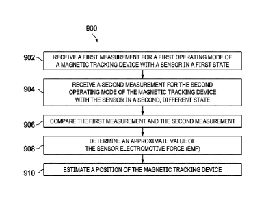
FIG. 9 shows an example of a process 900 for controlling a magnetic tracking
device (e.g., magnetic tracking device 200, 600, 700, 800, etc.) for sensor
parasitic loop
compensation of the magnetic tracking device. The process includes
determining, by a
processing device (e.g., of computing device 108 of FIG. 1), an approximate
value of a
sensor EMF of the magnetic tracking device. To determine the sensor EMF, the
processing device is configured to receive (902) a first measurement for a
first operating
mode of a magnetic tracking device with a sensor in a first state. In some
implementations, the first operating mode can include an ON state or activated
state of
the magnetic sensor (e.g., magnetic sensor 212, 612, 712, etc.). In some
implementations,
the first operating mode comprises a high sensitivity state of the magnetic
sensor (e.g.,
magnetic sensor 812). In some implementations, the processing device can
control a
switching device or other mechanism, such as biasing a diode, to control the
magnetic
tracking device to be in the first operating state.
The process 900 includes receiving (904) a second measurement for the second
operating mode of the magnetic tracking device with the sensor in a second,
different
state. In some implementations, the second operating mode can include an OFF
state or
deactivated state of the magnetic sensor (e.g., magnetic sensor 212, 612, 712,
etc.), such
that the sensor coil EMF is reduced or changed. In some implementations, the
second
operating mode comprises a low sensitivity state of the magnetic sensor (e.g.,
magnetic
sensor 812). In some implementations, the processing device can control a
switching
23
Date Recue/Date Received 2021-06-09
device or other mechanism, such as biasing a diode or setting a current to the
sensing
coil, to control the magnetic tracking device to be in the second operating
state.
The process 900 comprises comparing (906) the first measurement and the second
measurement. Comparing the first measurement and the second measurement can
include
comparing EMF values measured by the processing device, such as using a
differential
amplifier, in each operating mode of the magnetic tracking device. In some
implementations, an adjustment can be made to account for a change in
impedance in a
portion of the magnetic tracking device when changing the modes for the
comparison.
The process 900 includes determining (908) an approximate value of the sensor
electromotive force (EMF) of the magnetic sensor of the magnetic tracking
device. The
approximate value is based on the comparison. In some implementations, the
processor
uses the approximate value of the sensor EMF to estimate (910) a position of
the
magnetic tracking device, such as a position relative to a magnetic signal
transmitter. In
some implementations, the magnetic tracking device is inside a patient or near
a patient
during the process 900.
FIG. 10 is a block diagram of an example computer system 1000. The computing
system 108 described in relation to FIGS. 1-9 may be an example of the
computer system
1000 described here. The system 1000 can include a processor 1010, a memory
1020, a
storage device 1030, and an input/output device 1040. Each of the components
1010,
1020, 1030, and 1040 can be interconnected, for example, using a system bus
1050. The
processor 1010 is capable of processing instructions for execution within the
system
1000. The processor 1010 can be a single-threaded processor, a multi-threaded
processor,
or a quantum computer. The processor 1010 is capable of processing
instructions stored
in the memory 1020 or on the storage device 1030. The processor 1010 may
execute
operations such as causing the magnetic tracking system 100 to determine the
position
and/or the orientation of tracked device 200, 300, 600, 700, etc.
The memory 1020 stores information within the system 1000. In some
implementations, the memory 1020 is a computer-readable medium. The memory
1020
can, for example, be a volatile memory unit or a non-volatile memory unit.
24
Date Recue/Date Received 2021-06-09
The storage device 1030 is capable of providing mass storage for the system
1000. In an aspect, the storage device 1030 is a non-transitory computer-
readable
medium. The storage device 1030 can include, for example, a hard disk device,
an optical
disk device, a solid-date drive, a flash drive, magnetic tape, or some other
large capacity
storage device. The storage device 1030 may alternatively be a cloud storage
device, e.g.,
a logical storage device including multiple physical storage devices
distributed on a
network and accessed using a network. In some implementations, the information
stored
on the memory 1020 can also or instead be stored on the storage device 1030.
The input/output device 1040 provides input/output operations for the system
1000. In some examples, the input/output device 1040 includes one or more of
network
interface devices (e.g., an Ethernet card), a serial communication device
(e.g., an RS-232
10 port), and/or a wireless interface device (e.g., a short-range wireless
communication
device, an 602.11 card, a 3G wireless modem, or a 4G wireless modem).
Generally, the
input/output device 1040 includes driver devices configured to receive input
data and
send output data to other input/output devices, e.g., a keyboard, a printer,
and display
devices. In some implementations, mobile computing devices, mobile
communication
devices, and other devices are used.
The system 1000 can include a microcontroller. A microcontroller is a device
that
contains multiple elements of a computer system in a single electronics
package. For
example, the single electronics package could contain the processor 1010, the
memory
1020, the storage device 1030, and input/output devices 1040.
Although an example computer system has been described in FIG. 10,
implementations of the subject matter and the functional operations described
above can
be implemented in other types of digital electronic circuitry, or in computer
software,
firmware, or hardware, including the structures disclosed in this
specification and their
structural equivalents, or in combinations of one or more of them.
Implementations of the
subject matter described in this specification can be implemented as one or
more
computer program products, i.e., one or more modules of computer program
instructions
encoded on a tangible program carrier, for example a computer-readable medium,
for
.. execution by, or to control the operation of, a processing system. The
computer readable
Date Recue/Date Received 2021-06-09
medium can be a machine readable storage device, a machine readable storage
substrate,
a memory device, a composition of matter effecting a machine readable
propagated
signal, or a combination of one or more of them.
The term "computer system" may encompass all apparatus, devices, and machines
for processing data, including by way of example a programmable processor, a
computer,
or multiple processors or computers. A processing system can include, in
addition to
hardware, code that creates an execution environment for the computer program
in
question, e.g., code that constitutes processor firmware, a protocol stack, a
database
management system, an operating system, or a combination of one or more of
them.
A computer program (also known as a program, software, software application,
script, executable logic, or code) can be written in any form of programming
language,
including compiled or interpreted languages, or declarative or procedural
languages, and
it can be deployed in any form, including as a standalone program or as a
module,
component, subroutine, or other unit suitable for use in a computing
environment. A
computer program does not necessarily correspond to a file in a file system. A
program
can be stored in a portion of a file that holds other programs or data (e.g.,
one or more
scripts stored in a markup language document), in a single file dedicated to
the program
in question, or in multiple coordinated files (e.g., files that store one or
more modules,
sub programs, or portions of code). A computer program can be deployed to be
executed
on one computer or on multiple computers that are located at one site or
distributed
across multiple sites and interconnected by a communication network.
Computer readable media suitable for storing computer program instructions and
data include all forms of non-volatile or volatile memory, media and memory
devices,
including by way of example semiconductor memory devices, e.g., EPROM, EEPROM,
and flash memory devices; magnetic disks, e.g., internal hard disks or
removable disks or
magnetic tapes; magneto optical disks; and CD-ROM and DVD-ROM disks. The
processor and the memory can be supplemented by, or incorporated in, special
purpose
logic circuitry. The components of the system can be interconnected by any
form or
medium of digital data communication, e.g., a communication network. Examples
of
26
Date Recue/Date Received 2021-06-09
communication networks include a local area network ("LAN") and a wide area
network
("WAN"), e.g., the Internet.
A number of embodiments have been described. Nevertheless, it will be
understood that various modifications may be made without departing from the
spirit and
scope of the subject matter described herein. Other such embodiments are
within the
scope of the following claims.
27
Date Recue/Date Received 2021-06-09