Note: Descriptions are shown in the official language in which they were submitted.
CA 03122913 2021-06-10
WO 2020/121252 PCT/IB2019/060723
MASS SPECTROMETER COMPONENTS INCLUDING PROGRAMMABLE
ELEMENTS AND DEVICES AND SYSTEMS USING THEM
[001] PRIORITY APPLICATION
[002] This application is related to, and claims priority to and the benefit
of, U.S. Provisional
Application No. 62/779,419 filed on December 13, 2018, the entire disclosure
of which is hereby
incorporated herein by reference for all purposes.
[003] TECHNOLOGICAL FIELD
[004] Certain embodiments described herein are directed to mass spectrometer
programmable
elements. More particularly, certain configurations described herein are
directed to mass spectrometer
components that can be individually programmed to provide a desired feature or
result.
[005] BACKGROUND
[006] Mass spectrometers can be used to analyze ions based on differences in
mass-to-charge ratios
for different ions. Mass spectrometers include various components that can
perform different
functions.
[007] SUMMARY
[008] Certain aspects, features, embodiments and configurations are described
in reference to mass
spectrometer programmable elements (MSPE's). While the exact configuration of
the mass
spectrometer programmable element may vary, the mass spectrometer programmable
element
generally comprises at least one programmable element which can be controlled
separately from, e.g.,
independently of, an underlying component or substrate to which the
programmable element is
coupled.
[009] In one aspect, a mass spectrometer component comprises a substrate and
at least one mass
spectrometer programmable element, e.g., at least one programmable electrode,
disposed on the
substrate. In some examples, the at least one programmable electrode is
electrically decoupled from
the substrate. In some instances, the at least one programmable electrode is
configured to provide an
electric field within a space that is configured to receive an ion. In certain
examples, the substrate of
the mass spectrometer component is configured as a skimmer cone, and the
skimmer cone comprises
the at least one programmable electrode disposed on a surface of the skimmer
cone. In other examples,
the substrate of the mass spectrometer component is configured as a sampling
cone, and the sampling
cone comprises the at least one programmable electrode disposed on a surface
of the sampling cone.
In some embodiments, the substrate of the mass spectrometer component is
configured as one ion pole
of an ion deflector, and the one pole comprises the at least one programmable
electrode disposed on a
surface of the ion pole. In other examples, the substrate of the mass
spectrometer component is
1
CA 03122913 2021-06-10
WO 2020/121252 PCT/IB2019/060723
configured as a lens, and the lens comprises the at least one programmable
electrode disposed on a
surface of the lens. In further examples, the substrate of a mass spectrometer
component is configured
as a rod of a collision-reaction cell, and the rod comprises the at least one
programmable electrode
disposed on a surface of the rod. In some configurations, the substrate of the
mass spectrometer
component is configured as a mass analyzer comprising at least one rod set,
wherein one rod of the at
least one rod set comprises the at least one programmable electrode disposed
on a surface of the one
rod. In other configurations, the substrate of the mass spectrometer component
is configured as a lens
of a time of flight analyzer, and the lens comprises the at least one
programmable electrode disposed
of a surface of the lens. In some embodiments, the substrate of the mass
spectrometer component is
configured as an ion trap, and the ion trap comprises the at least one
programmable electrode disposed
on a surface of the ion trap. In other embodiments, the substrate of the mass
spectrometer component
is configured as a planar ion guide comprising the at least one programmable
electrode.
[010] In certain examples, the substrate of the mass spectrometer component is
configured as an
induction device, and the induction device comprises the at least one
programmable electrode disposed
on a surface of the induction device. In other examples, the substrate of the
mass spectrometer
component is configured as a torch, and the torch comprises the at least one
programmable electrode
disposed on a surface of the torch.
[011] In some examples, the substrate of the mass spectrometer component is
configured as an
injector, and the injector comprises the at least one programmable electrode
disposed on an outer
surface of the injector. In other embodiments, the substrate of the mass
spectrometer component is
configured as a nebulizer, and the nebulizer comprises the at least one
programmable electrode
disposed on a surface of the nebulizer. In certain embodiments, the substrate
of the mass spectrometer
component is configured as a spray chamber, and the spray chamber comprises
the at least one
programmable electrode disposed on a surface of the spray chamber.
[012] In certain examples, the substrate of the mass spectrometer component is
configured as a drift
tube comprising the at least one programmable electrode disposed on a surface
of a focusing ring of
the drift tube.
[013] In some examples, the mass spectrometer component further comprises an
additional MSPE,
e.g., an additional programmable electrode, disposed on the substrate and
electrically decoupled from
the substrate. In some configurations, the at least one programmable electrode
and the additional
programmable electrode are together configured to provide an electric field
within the space that is
configured to receive the ion.
[014] In some examples where two or more MSPE's are present, the substrate of
the mass
spectrometer component is configured as a skimmer, and the skimmer cone
comprises the at least one
programmable electrode and the additional programmable electrode each disposed
on a surface of the
skimmer cone. In other examples where two or more MSPE's are present, the
substrate of the mass
2
CA 03122913 2021-06-10
WO 2020/121252 PCT/1B2019/060723
spectrometer component is configured as a sampling cone, and the sampling cone
comprises the at
least one programmable electrode and the additional programmable electrode
each disposed on a
surface of the sampling cone. In additional examples where two or more MSPE's
are present, the
substrate of the mass spectrometer component is configured as one pole of an
ion deflector, and the
one pole comprises the at least one programmable electrode and the additional
programmable
electrode each disposed on a surface of the one pole. In certain embodiments
where two or more
MSPE's are present, the substrate of the mass spectrometer component is
configured as a lens, and the
lens comprises the at least one programmable electrode and the additional
programmable electrode
each disposed on a surface of the lens. In other embodiments where two or more
MSPE's are present,
the substrate of the mass spectrometer component is configured as one rod of a
collision-reaction cell,
and the one rod comprises the at least one programmable electrode and the
additional programmable
electrode each disposed on a surface of the one rod. In certain embodiments
where two or more
MSPE's are present, the substrate of the mass spectrometer component is
configured as a mass
analyzer comprising at least one rod set, wherein one rod of the at least one
rod set comprises the at
least one programmable electrode and the additional programmable electrode
each disposed on a
surface of the one rod. In some embodiments where two or more MSPE's are
present, the substrate
of the mass spectrometer component is configured as a lens of a time of flight
analyzer, and the lens
comprises the at least one programmable electrode and the additional
programmable electrode each
disposed on a surface of the lens. In other examples where two or more MSPE's
are present, the
substrate of the mass spectrometer component is configured as an ion trap, and
the ion trap the at least
one programmable electrode and the additional programmable electrode each
disposed on a surface of
the ion trap. In certain configurations where two or more MSPE's are present,
the substrate of the mass
spectrometer component is configured as a planar ion guide comprising the at
least one programmable
electrode and the additional programmable electrode.
[015] In certain examples where two or more MSPE's are present, the substrate
of the mass
spectrometer component is configured as an induction device, and the induction
device comprises the
at least one programmable electrode and the additional programmable electrode
each disposed on a
surface of the induction device. In some examples where two or more MSPE's are
present, the
substrate of the mass spectrometer component is configured as a torch, and the
torch comprises the at
least one programmable electrode and the additional programmable electrode
each disposed on a
surface of the torch.
[016] In other examples where two or more MSPE's are present, the substrate of
the mass
spectrometer component is configured as an injector, and the injector
comprises the at least one
programmable electrode and the additional programmable electrode each disposed
on an outer surface
of the injector. In certain configurations where two or more MSPE's are
present, the substrate of the
mass spectrometer component is configured as a nebulizer, and the nebulizer
comprises the at least
3
CA 03122913 2021-06-10
WO 2020/121252 PCT/1B2019/060723
one programmable electrode and the additional programmable electrode each
disposed on a surface of
the nebulizer. In some configurations where two or more MSPE's are present,
the substrate of the
mass spectrometer component is configured as a spray chamber, and the spray
chamber comprises the
at least one programmable electrode and the additional programmable electrode
each disposed on a
surface of the spray chamber. In other configurations where two or more MSPE's
are present, the
substrate of the mass spectrometer component is configured as a drift tube
comprising the at least one
programmable electrode and the additional programmable electrode each disposed
on a surface of a
focusing ring of the drift tube.
[017] In other instances, the mass spectrometer component may comprise a MSPE
array, e.g., an
electrode array comprising a plurality of separate and individually
programmable electrodes, each
disposed on the substrate. In some examples, the at least one programmable
electrode is an electrode
of the electrode array and is configured to provide the electric field within
the space that is configured
to receive the ion.
[018] In some examples where an MSPE array is present, the substrate of the
mass spectrometer
component is configured as a skimmer cone, and the skimmer cone comprises at
least one
programmable electrode disposed on a surface of the skimmer cone. In other
examples where an MSPE
array is present, the substrate of the mass spectrometer component is
configured as a sampling cone,
and the sampling cone comprises the at least one programmable electrode
disposed on a surface of the
sampling cone. In further examples where an MSPE array is present, the
substrate of the mass
spectrometer component is configured as one ion pole of an ion deflector, and
the one pole comprises
the at least one programmable electrode disposed on a surface of the ion pole.
In some examples where
an MSPE array is present, the substrate of the mass spectrometer component is
configured as a lens,
and the lens comprises the at least one programmable electrode disposed on a
surface of the lens. In
other examples where an MSPE array is present, the substrate of a mass
spectrometer component is
configured as a rod of a collision-reaction cell, and the rod comprises the at
least one programmable
electrode disposed on a surface of the rod. in certain configurations where an
MSPE array is present,
the substrate of the mass spectrometer component is configured as a mass
analyzer comprising at least
one rod set, wherein one rod of the at least one rod set comprises the at
least one programmable
electrode disposed on a surface of the one rod. In some configurations where
an MSPE array is
present, the substrate of the mass spectrometer component is configured as a
lens of a time of flight
analyzer, and the lens comprises the at least one programmable electrode
disposed of a surface of the
lens. in other configurations where an MSPE array is present, the substrate of
the mass spectrometer
component is configured as an ion trap, and the ion trap comprises the at
least one programmable
electrode disposed on a surface of the ion trap. In certain examples where an
MSPE array is present,
the substrate of the mass spectrometer component is configured as a planar ion
guide comprising the
at least one programmable electrode.
4
CA 03122913 2021-06-10
WO 2020/121252 PCT/1B2019/060723
[019] In certain configurations where an MSPE array is present, the substrate
of the mass
spectrometer component is configured as an induction device, and the induction
device comprises the
at least one programmable electrode disposed on a surface of the induction
device. In some
configurations where an MSPE array is present, the substrate of the mass
spectrometer component is
configured as a torch, and the torch comprises the at least one programmable
electrode disposed on a
surface of the torch.
[020] In additional configurations where an MSPE array is present, the
substrate of the mass
spectrometer component is configured as an injector and the injector comprises
the at least one
programmable electrode disposed on an outer surface of the injector. In
certain examples where an
MSPE array is present, the substrate of the mass spectrometer component is
configured as a nebulizer,
and the nebulizer comprises the at least one programmable electrode disposed
on a surface of the
nebulizer. In other examples where an MSPE array is present, the substrate of
the mass spectrometer
component is configured as a spray chamber, and the spray chamber comprises
the at least one
programmable electrode disposed on a surface of the spray chamber.
[021] In some examples, the electrode array comprises a plurality of planar
electrodes of about the
same thickness.
[022] In other examples, the electrode array comprises a plurality of
electrodes arranged in layers of
different heights with respect to a surface of the substrate.
[023] In some embodiments, the electrode array comprises a plurality of
electrodes arranged in
circumferential rings around a surface of the substrate. In additional
examples, the plurality of
electrodes arranged in the circumferential rings comprise different sized
electrodes. In some
examples, the electrodes in a first circumferential ring are electrically
coupled to each other through a
resistor network.
[024] In another aspect, a mass spectrometer component comprises a
programmable substrate and at
least one MSPE, e.g., at least one programmable electrode, disposed on the
programmable substrate.
In some examples, the at least one programmable electrode is electrically
decoupled from the
programmable substrate, and wherein the at least one programmable electrode is
configured to provide
an electric field within a space that is configured to receive an ion.
[025] In certain examples, the programmable substrate is configured to provide
a convex surface
upon application of a voltage to the programmable substrate. In other
examples, the programmable
substrate is configured to provide a concave surface upon application of a
voltage to the programmable
substrate. In some examples, the programmable substrate is configured to
provide a convex surface
upon application of a magnetic field to the programmable substrate. In certain
embodiments, the
programmable substrate is configured to provide a concave surface upon
application of a magnetic
field to the programmable substrate. In some examples, the programmable
substrate is configured to
provide a convex surface upon application of heat to the programmable
substrate. In other instances,
CA 03122913 2021-06-10
WO 2020/121252 PCT/1B2019/060723
the programmable substrate is configured to provide a concave surface upon
application of heat to the
programmable substrate. In some examples, the programmable substrate is
configured to provide a
convex surface upon application of pressure to the programmable substrate. In
other examples, the
programmable substrate is configured to provide a concave surface upon
application of pressure to the
programmable substrate.
[026] In further examples, the programmable substrate comprises a shape-memory
polymer or a
shape-memory alloy. In some examples, the programmable substrate comprises a
dielectric elastomer.
[027] In some configurations, the programmable substrate of the mass
spectrometer component is
programmed as a skimmer cone, and the skimmer cone comprises at least one
MSPE, e.g., at least one
programmable electrode, disposed on a surface of the skimmer cone. In other
configurations, the
programmable substrate of the mass spectrometer component is programmed as a
sampling cone, and
the sampling cone comprises at least one MSPE, e.g., at least one programmable
electrode, disposed
on a surface of the sampling cone. In certain examples, the programmable
substrate of the mass
spectrometer component is programmed as one ion pole of an ion deflector, and
the one pole comprises
at least one MSPE, e.g., at least one programmable electrode, disposed on a
surface of the ion pole.
In some embodiments, the programmable substrate of the mass spectrometer
component is
programmed as a lens, and the lens comprises at least one MSPE, e.g., at least
one programmable
electrode disposed on a surface of the lens. In certain examples, the
programmable substrate of a mass
spectrometer component is programmed as a rod of a collision-reaction cell,
and the rod comprises at
least one MSPE, e.g., at least one programmable electrode disposed on a
surface of the rod. In other
examples, the programmable substrate of the mass spectrometer component is
programmed as one rod
of a mass analyzer comprising at least one rod set, wherein the one rod of the
at least one rod set
comprises at least one MSPE, e.g. at least one programmable electrode disposed
on a surface of the
one rod. In some embodiments, the programmable substrate of the mass
spectrometer component is
programmed as a lens of a time of flight analyzer, and the lens comprises at
least on MSPE, e.g., at
least one programmable electrode disposed of a surface of the lens. In other
examples, the
programmable substrate of the mass spectrometer component is configured as an
ion trap, and the ion
trap comprises at least one MSPE, e.g., at least one programmable electrode
disposed on a surface of
the ion trap.
[028] In other embodiments, the programmable substrate of the mass
spectrometer component is
programmed as an induction device, and the induction device comprises at least
one MSPE, e.g., at
least one programmable electrode disposed on a surface of the induction
device. In some examples,
the programmable substrate of the mass spectrometer component is programmed as
a torch, and the
torch comprises at least one MSPE, e.g., at least one programmable electrode
disposed on a surface of
the torch.
6
CA 03122913 2021-06-10
WO 2020/121252 PCT/1B2019/060723
[029] In other examples, the substrate of the mass spectrometer component is
programmed as an
injector, and the injector comprises at least one MSPE, e.g., at least one
programmable electrode,
disposed on an outer surface of the injector. In certain embodiments, the
substrate of the mass
spectrometer component is programmed as a nebulizer, and the nebulizer
comprises at least one
MSPE, e.g., at least one programmable electrode disposed on a surface of the
nebulizer. In other
examples, the substrate of the mass spectrometer component is programmed as a
spray chamber, and
the spray chamber comprises at least one MSPE, e.g., at least one programmable
electrode disposed
on a surface of the spray chamber. In other examples, the programmable
substrate of the mass
spectrometer component is programmed as a focusing ring of a drift tube, and
the drift tube comprises
the at least one programmable electrode disposed on a surface of the drift
tube. In some examples, the
substrate of the mass spectrometer component is programmed as a planar ion
guide comprising at least
one MSPE, e.g., at least one programmable electrode.
[030] In other instances, the mass spectrometer component comprises at least
one additional MSPE,
e.g., at least one additional programmable electrode, disposed on the
programmable substrate and
electrically decoupled from the programmable substrate, wherein the at least
one programmable
electrode and the at least one additional programmable electrode are together
configured to provide
an electric field within the space that is configured to receive the ion.
[031] In some embodiments, the programmable substrate of the mass spectrometer
component is
programmed as a skimmer, and the skimmer cone comprises the at least one
programmable electrode
and the additional programmable electrode each disposed on a surface of the
skimmer cone. In other
embodiments, the programmable substrate of the mass spectrometer component is
programmed as a
sampling cone, and the sampling cone comprises the at least one programmable
electrode and the
additional programmable electrode each disposed on a surface of the sampling
cone.
[032] In certain examples, the programmable substrate of the mass spectrometer
component is
programmed as one pole of an ion deflector, and the one pole comprises the at
least one programmable
electrode and the additional programmable electrode each disposed on a surface
of the one pole. In
some examples, the programmable substrate of the mass spectrometer component
is programmed as a
lens, and the lens comprises the at least one programmable electrode and the
additional programmable
electrode each disposed on a surface of the lens. In some embodiments, the
programmable substrate
of the mass spectrometer component is programmed as one rod of a collision-
reaction cell, and the
one rod comprises the at least one programmable electrode and the additional
programmable electrode
each disposed on a surface of the one rod. In other embodiments, the
programmable substrate of the
mass spectrometer component is programmed as one rod of a mass analyzer
comprising at least one
rod set, wherein the one rod of the at least one rod set comprises the at
least one programmable
electrode and the additional programmable electrode each disposed on a surface
of the one rod. In
other examples, the programmable substrate of the mass spectrometer component
is programmed as a
7
CA 03122913 2021-06-10
WO 2020/121252 PCT/1B2019/060723
lens of a time of flight analyzer, and the lens comprises the at least one
programmable electrode and
the additional programmable electrode each disposed on a surface of the lens.
In certain examples,
the programmable substrate of the mass spectrometer component is programmed as
an ion trap, and
the ion trap the at least one programmable electrode and the additional
programmable electrode each
disposed on a surface of the ion trap. In other instances, the programmable
substrate of the mass
spectrometer component is programmed as a planar ion guide comprising the at
least one
programmable electrode and the additional programmable electrode.
[033] In some examples, the programmable substrate of the mass spectrometer
component is
programmed as an induction device, and the induction device comprises the at
least one programmable
electrode and the additional programmable electrode each disposed on a surface
of the induction
device. In other examples, the programmable substrate of the mass spectrometer
component is
programmed as a torch, and the torch comprises the at least one programmable
electrode and the
additional programmable electrode each disposed on a surface of the torch.
[034] In certain embodiments, the programmable substrate of the mass
spectrometer component is
programmed as an injector, and the injector comprises the at least one
programmable electrode and
the additional programmable electrode each disposed on an outer surface of the
injector. In some
examples, the programmable substrate of the mass spectrometer component is
programmed as a
nebulizer, and the nebulizer comprises the at least one programmable electrode
and the additional
programmable electrode each disposed on a surface of the nebulizer. In certain
examples, the
programmable substrate of the mass spectrometer component is programmed as a
spray chamber, and
the spray chamber comprises the at least one programmable electrode and the
additional
programmable electrode each disposed on a surface of the spray chamber. In
other examples, the
programmable substrate of the mass spectrometer component is programmed as a
focusing ring of a
drift tube, and the drift tube comprises the at least one programmable
electrode and the additional
programmable electrode each disposed on a surface of the drift tube.
[035] In certain embodiments, a mass spectrometer component comprising a
programmable
substrate may comprise an electrode array comprising a plurality of separate
and individually
programmable electrodes each disposed on the programmable substrate, wherein
the at least one
programmable electrode is an electrode of the electrode array and is
configured to provide the electric
field within the space that is configured to receive the ion. In certain
examples, the electrode array
comprises a plurality of planar electrodes of about a same thickness. In other
examples, the electrode
array comprises a plurality of planar electrodes of a different thickness. In
some embodiments, the
electrode array comprises a plurality of electrodes arranged in layers of
different heights with respect
to a surface of the programmable substrate. In certain examples, the electrode
array comprises a
plurality of electrodes arranged in circumferential rings around a surface of
the programmable
substrate. In other examples, the plurality of electrodes arranged in the
circumferential rings
8
CA 03122913 2021-06-10
WO 2020/121252 PCT/1B2019/060723
comprises different sized electrodes. In some embodiments, the electrodes in a
first circumferential
ring are electrically coupled to each other through a resistor network. In
certain examples, electrodes
in adjacent circumferential rings are programmed with different voltages. In
some examples,
electrodes in a circumferential ring are programmed with different voltages.
In other examples,
electrodes of the electrode array are individually programmed with a DC
voltage.
[036] In another aspect, a mass spectrometer skimmer cone configured to
receive ions from an
ionization source fluiclically coupled to the mass spectrometer skimmer cone
is described. In some
examplesõ the mass spectrometer skimmer cone comprises a tapered member
comprising a distal
aperture configured to receive the ions from the ionization source and provide
the received ions to a
downstream component, the skimmer cone comprising at least one programmable
electrode on a
surface of the tapered member and electrically decoupled from the surface of
the tapered member, and
wherein the at least one programmable electrode is configured to provide an
electric field within a
space between the skimmer cone and the ionization source.
[037] In certain examples, the tapered member comprises a programmable
substrate. In other
examples, the skimmer cone comprises at least one additional programmable
electrode disposed on
the surface of the tapered member. In some embodiments, the skimmer cone
comprises an array of
programmable electrodes disposed on the surface of the tapered member. In some
examples, the
skimmer cone comprises an insulating material disposed between the
programmable electrode and the
surface.
[038] In an additional aspect, a mass spectrometer sampling interface
configured to receive ions is
described. In some examples, the mass spectrometer sampling interface
comprises a housing
comprising a sampling inlet, the housing comprising at least one programmable
electrode on an
incident surface of the housing and electrically decoupled from the incident
surface of the housing,
and wherein the at least one programmable electrode is configured to provide
an electric field adjacent
to the incident surface of the mass spectrometer sampling interface.
[039] In some embodiments, the housing comprises a programmable substrate. In
other
embodiments, at least one additional programmable electrode is disposed on the
incident surface. In
certain examples, an array of programmable electrodes is disposed on the
incident surface. In some
examples, an insulating material is disposed between the programmable
electrode and the incident
surface.
[040] In another aspect, an ion guide comprises a first multipole comprising a
plurality of separate
poles, wherein at least one pole of the first multipole comprises a
programmable electrode on a surface
of the at least one pole, wherein the programmable electrode is electrically
decoupled from the at least
one pole, the first multipole having a first opening and a second opening
fluidically coupled to the first
opening, wherein the programmable electrode is configured to provide an
electric field within a space
formed by the plurality of separate poles, and wherein the electric field is
effective to alter a first
9
CA 03122913 2021-06-10
WO 2020/121252 PCT/1B2019/060723
trajectory of ions entering the first multipole through the first opening to a
second trajectory to permit
the ions of the second trajectory to exit the first multipole through the
second opening.
[041] In certain examples, each of the plurality of separate poles comprises a
plurality of
programmable electrodes disposed on a surface of each of the plurality of
separate poles, and wherein
a DC voltage provided to the electrodes of each of the plurality of separate
poles is effective to provide
a DC electric field within the space formed by the plurality of separate
poles. In some embodiments,
each of the plurality of separate poles comprises a non-conductive substrate.
In other examples, each
of the plurality of separate poles is electrically decoupled from the
plurality of programmable
electrodes through an insulating material. In some examples, each electrode of
a circumferential
electrode ring on the one pole is electrically coupled to each other through a
resistor network. In
certain embodiments, an insulating material is disposed between the surface of
the at least one pole
and the programmable electrode. In other embodiments, a linear array of
programmable electrodes is
disposed on the surface of the at least one pole. In some examples, an
insulating material is disposed
between each electrode of the linear array of programmable electrodes and the
surface of the at least
one pole.
[042] In some examples, a power source is electrically coupled to the
programmable electrode. In
other examples, the power source is configured to provide one or more of a DC
voltage, an AC voltage,
and an RF voltage.
[043] In another aspect, a cell configured to fluidically couple to an
ionization source at an entrance
aperture to receive ions into the cell and configured to provide ions from the
cell through an exit
aperture fluidically coupled to a mass analyzer is disclosed. In some
examples, the cell comprises a
gas inlet configured to receive a gas in a collision mode to pressurize the
cell and configured to receive
a reaction gas in a reaction mode, the cell further comprising a rod set,
wherein at least one rod of the
rod set comprises a programmable electrode on a surface of the at least one
rod of the rod set, and
wherein the programmable electrode is electrically decoupled from the at least
one rod.
[044] In certain examples, the programmable electrode is configured to provide
a DC electric field
within a space formed by the rod set when a DC voltage is provided to the
programmable electrode.
In other examples, each rod of the rod set comprises a plurality of
programmable electrodes disposed
on a surface of each rod, and wherein a DC voltage provided to the electrodes
on each rod is effective
to provide the DC electric field within the space formed by the rod set. In
some embodiments, an
insulating material is present between the programmable electrode and the at
least one rod. In other
examples, the at least one rod is configured as a programmable substrate.
[045] In an additional aspect, an ion lens comprises a planar substrate
comprising a first surface and
a second surface, and a programmable electrode on the first surface of the
planar substrate and
electrically decoupled from the first surface of the planar substrate, and
wherein the programmable
electrode is configured to provide an electric field within a space that is
configured to receive an ion.
CA 03122913 2021-06-10
WO 2020/121252 PCT/1B2019/060723
[046] In some examples, the planar substrate is configured as a printed
circuit board. In other
examples, the programmable electrode is an etched electrode on the printed
circuit board. In some
embodiments, an insulating material is present between the programmable
electrode and the first
surface. In other examples, the ion lens comprises an additional programmable
electrode on the first
surface. In some examples, each of the programmable electrode and the
additional programmable
electrode are configured as a ring electrode. in certain embodiments, an
insulating material is present
between each ring electrode and the first surface. In some examples, the ion
lens comprises a third
programmable electrode on the first surface. In some examples, an insulating
material between each
of the three ring electrodes and the first surface. In other examples, the ion
lens comprises a power
source electrically coupled to at least one ring electrode. In some
embodiments, the ion lens comprises
a first resistor configured to electrically couple the programmable electrode
and the additional
programmable electrode. In other examples, the ion lens comprises a second
resistor configured to
electrically couple the additional programmable electrode and the third
programmable electrode. In
some embodiments, the first resistor and second resistor are selected so a
voltage provided to the third
programmable electrode is greater than a voltage provided to the programmable
electrode. In other
embodiments, the first resistor and second resistor are selected so a voltage
provided to the
programmable electrode is greater than a voltage provided to the third
programmable electrode. In
some examples, the power source is configured to provide one or more of a DC
voltage, an AC voltage
and an RF voltage.
[047] In another aspect, a time of flight device comprises a flight tube, and
a lens assembly
comprising a plurality of independent lenses disposed in the flight tube,
wherein at least one lens of
the lens assembly comprises a programmable electrode electrically decoupled
from a substrate of the
at least one lens, and wherein the programmable electrode is configured to
provide an electric field
within a space of the lens assembly that is configured to receive an ion.
[048] In certain examples, the lens comprising the programmable electrode is
positioned proximate
to a detector. In other examples, the at least one lens further comprises at
least one additional
programmable electrode. In some examples, the at least one lens further
comprises a programmable
electrode array. In other examples, a second lens of the lens assembly
comprises at programmable
electrode. In some embodiments, each lens of the lens assembly comprises a
programmable electrode.
In other examples, an insulating material is present between the programmable
electrode and the at
least one lens. In some examples, the at least one lens is configured as a
programmable substrate. In
other embodiments, a power source is electrically coupled to the programmable
electrode. In some
examples, the power source is configured to provide one or more of a DC
voltage, an AC voltage and
an RF voltage to the programmable electrode.
[049] In an additional aspect, a reflectron comprises a plurality of
independent and substantially
parallel lenses positioned in a housing, wherein at least one lens comprises a
programmable electrode
11
CA 03122913 2021-06-10
WO 2020/121252 PCT/1B2019/060723
on a planar surface of the at least one ion lens, wherein the programmable
electrode is electrically
decoupled from the planar surface of the at least one lens, and wherein the
programmable electrode is
configured to provide an electric field within a space between lenses of the
reflectron.
[050] In some embodiments, the lens comprising the programmable electrode is
positioned
proximate to a detector. In some examples, the at least one lens further
comprises at least one
additional programmable electrode. in other embodiments, the at least one lens
further comprises a
programmable electrode array. In certain examples, a second lens of the lens
assembly comprises at
programmable electrode. In some embodiments, each lens of the lens assembly
comprises a
programmable electrode. In certain instances, an insulating material is
present between the
programmable electrode and the at least one lens. In other examples, the at
least one lens is configured
as a programmable substrate. In some embodiments, a power source is
electrically coupled to the
programmable electrode. In other examples, the power source is configured to
provide one or more
of a DC voltage, an AC voltage and an RE voltage to the programmable
electrode.
[051] In another aspect, a mass analyzer comprises a plurality of rods each
positioned substantially
parallel to each other, wherein at least one rod comprises a programmable
electrode on a surface of
the at least one rod, wherein the programmable electrode is electrically
decoupled from the at least
one rod, and wherein the programmable electrode is configured to provide an
electric field within a
space formed by the positioned rods.
[052] In certain examples, the plurality of rods are arranged as a quadrupole,
and wherein the at least
one rod of the quadrupole comprises the programmable electrode on a surface.
In other examples, the
mass analyzer comprises a second programmable electrode on a surface of a
second rod of the
quadrupole. In other instances, the mass analyzer comprises a third
programmable electrode on a
surface of a third rod of the quadrupole. In further examples, the mass
analyzer comprises a fourth
programmable electrode on a surface of a fourth rod of the quadrupole. in some
examples, the mass
analyzer comprises a power source electrically coupled to each of the
programmable electrode, the
second programmable electrode, the third programmable electrode and the fourth
programmable
electrode. In further instances, the mass analyzer comprises an insulating
material present between
each of the programmable electrode and the at least one rod, between the
second programmable
electrode and the second rod, between the third programmable electrode and the
third rod and between
the fourth programmable electrode and the fourth rod. In some embodiments,
each rod of the
quadrupole is configured as a programmable substrate. In other examples, each
rod comprises a shape
memory polymer or a shape memory alloy. In some examples, the mass analyzer
comprises at least
one additional programmable electrode on the at least one rod.
[053] In another aspect, a dipole ion guide comprises a first set of
electrodes disposed on a first
substrate, and a second set of electrodes disposed on a second substrate
spatially separated from the
first substrate, wherein each electrode of the first set is independently
programmable and wherein each
12
CA 03122913 2021-06-10
WO 2020/121252 PCT/1B2019/060723
electrode of the second set is independently programmable, wherein the first
set and the electrodes of
the second set are configured to provide an electric field within a space
between the spatially separated
electrodes to guide an ion between the first substrate and the second
substrate.
[054] In certain configurations, a central electrode of the first set of
electrodes and a central electrode
of the second set of electrodes are each programmed to trap the ion within the
dipole ion guide. In
some embodiments, the central electrode of the first set of electrodes and the
central electrode of the
second set of electrodes are each programmed with an RE voltage. In other
embodiments, wherein
electrodes adjacent to the central electrode of the first set of electrodes
and electrodes adjacent to the
central electrode of the second set of electrodes are programmed to be more
positively charged. In
other examples, a central electrode of the first set of electrodes and a
central electrode of the second
set of electrodes are each programmed with differential RE and DC voltages to
filter ions provided to
the dipole ion guide. In some embodiments, each of the first substrate and the
second substrate is
configured as a programmable substrate. In further examples, the first set of
electrodes is configured
as an array of linear electrodes. In some examples, the second set of
electrodes is configured as an
array of linear electrodes. In further embodiments, the dipole ion guide
comprises a power source
electrically coupled to each of the first set of electrodes and the second set
of electrodes. In some
instances, the power source is configured to provide one or more of a DC
voltage, an AC voltage, an
RF voltage or combinations thereof.
[055] In another aspect, an ion switch comprises a first ion guide fluidically
coupled to a first ion
source, the first ion guide comprising a first substrate spatially positioned
from a second substrate,
wherein each of the first substrate and the second substrate of the first ion
guide comprise a respective
set of electrodes, wherein each respective set of electrodes is electrically
decoupled from its respective
substrate, and wherein the electrodes on the first substrate and the
electrodes on the second substrate
are configured to provide an electric field within a space between the
spatially separated first and
second substrates. The ion switch may also comprise a second ion guide
fluidically coupled to a second
ion source, the second ion guide comprising a third substrate spatially
positioned from a fourth
substrate, wherein each of the third substrate and the fourth substrate of the
first ion guide comprise a
respective set of electrodes, wherein each respective set of electrodes is
electrically decoupled from
its respective substrate, and wherein the electrodes on the third substrate
and the electrodes on the
fourth substrate are configured to provide an electric field within a space
between the spatially
separated third and fourth substrates. The ion switch may also comprise a
processor configured to
provide a first respective voltage to each of the first ion guide and the
second ion guide to provide an
ion output from the first ion guide in a first mode of the ion switch and
block an ion output from the
second ion guide in the first mode of the ion switch, and wherein the
processor is configured to provide
a second respective voltage to each of the first ion guide and the second ion
guide to block an ion
13
CA 03122913 2021-06-10
WO 2020/121252 PCT/1B2019/060723
output from the first ion guide in a second mode of the ion switch and provide
an ion output from the
second ion guide in the second mode of the ion switch.
[056] In certain examples, a central electrode of the first set of electrodes
of the first ion guide and
a central electrode of the second set of electrodes of the first ion guide are
each programmed to trap
the ion within the first ion guide. In other examples, the central electrode
of the first of the first set of
electrodes on the first substrate of the first ion guide and the central
electrode of the second set of
electrodes on the second substrate of the first ion guide are each programmed
with an RF voltage. In
some embodiments, a central electrode of a first set of electrodes on the
third substrate of the second
ion guide and a central electrode of a second set of electrodes on the fourth
substrate of the second ion
guide are each programmed to trap the ion within the second ion guide. In
other examples, the central
electrode of a first set of electrodes on the third substrate of the second
ion guide and the central
electrode of a second set of electrodes on the fourth substrate of the second
ion guide are each
programmed with an RF voltage. In certain embodiments, electrodes adjacent to
the central electrode
of the first set of electrodes of the first ion guide and electrodes adjacent
to the central electrode of the
second set of electrodes of the first ion guide are programmed to be more
positively charged. In other
examples, a central electrode of the first set of electrodes of the first ion
guide and a central electrode
of the second set of electrodes of the first ion guide are each programmed
with differential RF and DC
voltages to filter ions provided to the ion switch. In some examples, each of
the first substrate and the
second substrate of the first ion guide is configured as a programmable
substrate. In other examples,
a first set of electrodes on the first substrate of the first ion guide and a
second set of electrodes on the
second substrate of the first ion guide are each configured as an array of
linear electrodes. In other
examples, a first set of electrodes on the third substrate and the second set
of electrodes on the fourth
substrate of the second ion guide are each configured as an array of linear
electrodes.
[057] Additional aspects, features, configurations and examples are described
in more detail below.
[058] BRIEF DESCRIPTION OF THE SEVERAL VIEWS OF THE DRAWINGS
[059] Certain illustrative representations, configurations and forms of a mass
spectrometer
programmable element are described with reference to the accompanying figures
in which:
[060] FIG. 1A is a block diagram of a mass spectrometer, in accordance with
certain embodiments;
[061] FIG. 1B is a block diagram of a mass spectrometer comprising an ion
source with a mass
spectrometer programmable element, in accordance with certain embodiments;
[062] FIG. 1C is a block diagram of a mass spectrometer comprising a mass
analyzer with a mass
spectrometer programmable element, in accordance with certain embodiments;
[063] FIG. 1D is a block diagram of a mass spectrometer comprising a detector
with a mass
spectrometer programmable element, in accordance with certain embodiments;
14
CA 03122913 2021-06-10
WO 2020/121252 PCT/1B2019/060723
[064] FIG. 1E is a block diagram of a mass spectrometer comprising an ion
source with a mass
spectrometer programmable element and a mass analyzer with a mass spectrometer
programmable
element, in accordance with certain embodiments;
[065] FIG. 1F is a block diagram of a mass spectrometer comprising an ion
source with a mass
spectrometer programmable element and a detector with a mass spectrometer
programmable element,
in accordance with certain embodiments;
[066] FIG. 1G is a block diagram of a mass spectrometer comprising a mass
analyzer with a mass
spectrometer programmable element and a detector with a mass spectrometer
programmable element,
in accordance with certain embodiments;
[067] FIG. 1H is a block diagram of a mass spectrometer comprising an ion
source with a mass
spectrometer programmable element, a mass analyzer with a mass spectrometer
programmable
element, and a detector with a mass spectrometer programmable element, in
accordance with certain
embodiments;
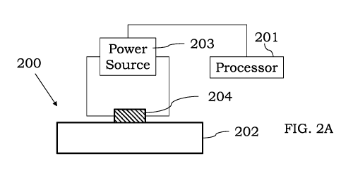
[068] FIG. 2A is an illustration showing a generalized mass spectrometer
programmable element, in
accordance with certain configurations;
[069] FIG. 2B is an illustration showing two mass spectrometer programmable
elements configured
as electrodes, in accordance with certain configurations;
[070] FIG 2C is an illustration showing three mass spectrometer programmable
elements configured
as electrodes, in accordance with certain examples;
[071] FIG. 2D is an illustration showing a mass spectrometer programmable
element configured as
a ring electrode, in accordance with certain embodiments;
[072] FIG. 2E is an illustration showing a mass spectrometer programmable
element configured as
a square electrode, in accordance with certain embodiments;
[073] FIG. 2F is an illustration showing a mass spectrometer programmable
element configured as
a triangular electrode, in accordance with certain embodiments;
[074] FIG. 2G is an illustration showing two mass spectrometer programmable
elements each
configured as ring electrodes, in accordance with certain embodiments,
[075] FIG. 2H is another illustration showing two mass spectrometer
programmable elements each
configured as ring electrodes, in accordance with certain embodiments;
[076] FIG. 21 an illustration showing mass spectrometer programmable elements
configured as an
electrode array, in accordance with certain embodiments;
[077] FIG. 2J an illustration showing mass spectrometer programmable elements
configured with
different heights, in accordance with certain embodiments;
[078] FIG. 2K an illustration showing stacked mass spectrometer programmable
elements, in
accordance with certain examples;
CA 03122913 2021-06-10
WO 2020/121252 PCT/1B2019/060723
[079] FIGS. 3A and 3B are illustrations of a programmable substrate, in
accordance with some
examples;
[080] FIGS. 4A, 4B and 4C show various layers of a mass spectrometer component
comprising at
least one mass spectrometer programmable element, in accordance with certain
embodiments;
[081] FIG. 5 is an illustration showing a generalized mass spectrometer system
comprising a sample
introduction device, in accordance with some configurations;
[082] FIG. 6 is an illustration showing a nebulizer comprising a mass
spectrometer programmable
element, in accordance with certain configurations;
[083] FIG. 7A is one illustration of a spray chamber comprising a mass
spectrometer programmable
element, in accordance with certain configurations;
[084] FIG. 7B is another illustration of a spray chamber comprising a mass
spectrometer
programmable element, in accordance with certain configurations;
[085] FIG. 8A is a block diagram showing a generalized schematic of an
inductively coupled plasma
ion source, in accordance with some examples;
[086] FIG. 8B is an illustration of an ion source showing an induction device
comprising a mass
spectrometer programmable element, in accordance with some examples;
[087] FIG. 9 is an illustration of an ion source showing a torch comprising a
mass spectrometer
programmable element, in accordance with some examples;
[088] FIG. 10 is an illustration of an ion source showing an interface
comprising a mass spectrometer
programmable element, in accordance with some examples;
[089] FIG 11 is an illustration of an inductively coupled plasma ion source
comprising a finned
induction coil comprising a mass spectrometer programmable element, in
accordance with some
embodiments;
[090] FIG. 12 is an illustration of an inductively coupled plasma ion source
comprising plate
electrodes at least one of which comprises a mass spectrometer programmable
element, in accordance
with certain examples;
[091] FIG. 13 is an illustration of an inductively coupled plasma ion source
comprising a cylindrical
induction device comprising a mass spectrometer programmable element, in
accordance with some
embodiments;
[092] FIG. 14 is an illustration of an electron ionization source comprising a
mass spectrometer
programmable element, in accordance with some examples;
[093] FIG. 15 is an illustration of a chemical ionization source comprising a
mass spectrometer
programmable element, in accordance with certain examples;
[094] FIG. 16 is an illustration of a field ionization source comprising a
mass spectrometer
programmable element, in accordance with some examples;
16
CA 03122913 2021-06-10
WO 2020/121252 PCT/1B2019/060723
[095] FIG. 17 is an illustration of a laser desorption ionization source
comprising a mass
spectrometer programmable element, in accordance with some examples;
[096] FIG. 18 is an illustration of a spray ionization source comprising a
mass spectrometer
programmable element, in accordance with some examples;
[097] FIG. 19 is an illustration of an interface comprising a mass
spectrometer programmable
element, in accordance with some examples;
[098] FIG. 20 is another illustration of a system comprising an interface
comprising a mass
spectrometer programmable element, in accordance with some examples;
[099] FIG. 21 is a general diagram showing some components present in a mass
analyzer, in
accordance with some examples;
[0100] FIG. 22 is an illustration of a lens comprising a mass spectrometer
programmable element, in
accordance with certain embodiments;
[0101] FIG. 23 is another illustration of a lens comprising a mass
spectrometer programmable
element, in accordance with certain examples;
[0102] FIG. 24 is an illustration of a lens comprising a mass spectrometer
programmable element, in
accordance with certain examples;
[0103] FIG. 25A is an illustration of an ion guide comprising a mass
spectrometer programmable
element, in accordance with certain embodiments;
[0104] FIG 25B is an illustration of an ion guide comprising two mass
spectrometer programmable
elements, in accordance with certain embodiments;
[0105] FIG 25C is an illustration of an ion guide comprising three mass
spectrometer programmable
elements, in accordance with certain embodiments;
[0106] FIG. 25D is an illustration of an ion guide comprising four mass
spectrometer programmable
elements, in accordance with certain embodiments;
[0107] FIG. 25E is an illustration of a dipolar ion guide comprising a
plurality of mass spectrometer
programmable elements, in accordance with certain embodiments;
[0108] FIG. 26 is an illustration of a collision cell (or collision/reaction
cell) comprising one or more
mass spectrometer programmable elements, in accordance with certain examples;
[0109] FIG. 27A is an illustration of a quadrupole mass analyzer comprising a
mass spectrometer
programmable element, in accordance with certain examples;
[0110] FIG. 27B is an illustration of a quadrupole mass analyzer comprising
two mass spectrometer
programmable elements, in accordance with certain examples;
[0111] FIG. 27C is an illustration of a quadrupole mass analyzer comprising
three mass spectrometer
programmable elements, in accordance with certain examples;
[0112] FIG. 27D is an illustration of a quadrupole mass analyzer comprising
four mass spectrometer
programmable elements, in accordance with certain examples;
17
CA 03122913 2021-06-10
WO 2020/121252 PCT/1B2019/060723
[0113] FIG. 28A is an illustration of a dual quadrupole mass analyzer where at
least one of the
quadrupoles comprises a mass spectrometer programmable element, in accordance
with certain
examples;
[0114] FIG. 28B another illustration of a dual quadrupole mass analyzer where
at least one of the
quadrupoles comprises a mass spectrometer programmable element, in accordance
with certain
examples;
[0115] FIG. 28C is an illustration of a dual quadrupole mass analyzer where
both the quadrupoles
comprise a mass spectrometer programmable element, in accordance with certain
examples:
[0116] FIGS. 29A, 29B, 29C, 29D, 29E, 29F and 29G are illustrations of a
triple quadrupole mass
analyzer where at least one of the quadrupole mass analyzers comprises a mass
spectrometer
programmable element, in accordance with certain examples;
[0117] FIG. 30 is an illustration of a linear ion trap comprising a mass
spectrometer programmable
element, in accordance with certain examples;
[0118] FIG. 31A is an illustration of a time of flight device with a mass
spectrometer programmable
element, in accordance with certain examples;
[0119] FIG. 31B is an illustration of a reflectron where at least one lens of
the reflectron comprises a
mass spectrometer programmable element, in accordance with certain examples;
[0120] FIG. 32 is an illustration of an ion mobility drift tube comprising a
mass spectrometer
programmable element, in accordance with some examples;
[0121] FIG. 33 is an illustration of an electron multiplier detector where at
least one dynode of the
electron multiplier comprises a mass spectrometer programmable element, in
accordance with certain
examples;
[0122] FIG. 34 is an illustration of a Faraday cup detector comprising a mass
spectrometer
programmable element, in accordance with certain examples;
[0123] FIG. 35 is an illustration of a microchannel plate detector comprising
a mass spectrometer
programmable element, in accordance with certain examples;
[0124] FIGS. 36A, 36B, 36C, 36D, 36E, 36F, and 36G are block diagrams of an
inductively coupled
plasma ion source coupled to a mass analyzer and a detector, in accordance
with some examples;
[0125] FIGS. 37A, 37B, 37C, 37D, 37E, 37F, and 37G are block diagrams of an
ion source other than
an inductively coupled plasma ion source that is coupled to a mass analyzer
and a detector, in
accordance with some examples;
[0126] FIG. 38 is an illustration of a gas chromatography device coupled to a
mass spectrometer
comprising a MS programmable element, in accordance with certain embodiments;
[0127] FIG. 39 is an illustration of a liquid chromatography device coupled to
a mass spectrometer
comprising a MS programmable element, in accordance with certain embodiments;
18
CA 03122913 2021-06-10
WO 2020/121252 PCT/IB2019/060723
[0128] FIG. 40 is an illustration showing a lens comprising a programmable
electrode with an
adjustable surface potential, in accordance with some examples;
[0129] FIG. 41 is another illustration showing MS programmable elements with
different voltages, in
accordance with some embodiments;
[0130] FIG. 42 is an illustration showing electric fields of MS programmable
elements with different
voltages, in accordance with some embodiments;
[0131] FIG. 43A is an illustration of a conventional lens, and FIG. 43B is a
simulation showing ion
distribution in an opening of the lens of FIG. 43A, in accordance with some
examples;
[0132] FIG. 44A is an illustration of a lens comprising three ring electrodes
as MS programmable
elements, and FIG. 44B is a simulation showing ion distribution in an opening
of the lens of FIG. 44A,
in accordance with some examples;
[0133] FIGS. 45A and 45B are intensity curves showing measurement of a lithium
sample using a
conventional lens (FIG. 45A) and a lens similar to the one shown in FIG. 44B
(FIG. 45B), in
accordance with certain embodiments;
[0134] FIGS. 46A and 46B are intensity curves showing measurement of a
magnesium sample using
a conventional lens (FIG. 46A) and a lens similar to the one shown in FIG. 44B
(FIG. 46B), in
accordance with certain embodiments;
[0135] FIGS. 47A and 47B are intensity curves showing measurement of an indium
sample using a
conventional lens (FIG. 47A) and a lens similar to the one shown in FIG. 44B
(FIG. 47B), in
accordance with certain embodiments;
[0136] FIGS. 48A and 48B are intensity curves showing measurement of a lead
sample using a
conventional lens (FIG. 48A) and a lens similar to the one shown in FIG. 44B
(FIG. 48B), in
accordance with certain embodiments;
[0137] FIGS. 49A and 49B are intensity curves showing measurement of a uranium
sample using a
conventional lens (FIG. 49A) and a lens similar to the one shown in FIG. 44B
(FIG. 49B), in
accordance with certain embodiments;
[0138] FIG. 50 is an illustration of an ion guide, in accordance with some
embodiments;
[0139] FIG. 51 is an illustration of an ion multiplexer, in accordance with
some examples;
[0140] FIG. 52 is another illustration of an ion multiplexer, in accordance
with some examples;
[0141] FIG. 53 is an illustration of a lens stack, in accordance with certain
configurations; and
[0142] FIG. 54 is an illustration of a system comprising an ion-on-demand
system, in accordance with
some examples.
[0143] It will be recognized by the person of ordinary skill in the art, given
the benefit of this
disclosure, that the components in the figures are provided merely for
illustration purposes and are not
necessarily the only representations which can be produced. The mass
spectrometer programmable
elements in the figures can adopt may different sizes, shapes, positions,
orientations and arrangements,
19
CA 03122913 2021-06-10
WO 2020/121252 PCT/I132019/060723
and the illustrative sizes, shapes, positions, orientations and arrangements
shown in the figures are not
required. in addition, the mass spectrometer programmable elements may be
exaggerated or otherwise
not drawn to scale to provide more user-friendly figures and to facilitate a
better understanding of the
technology described in this description.
[0144] DETAILED DESCRIPTION
[0145] Many different illustrations of mass spectrometer (MS) programmable
elements are discussed
below to illustrate some of the various configurations the MS programmable
elements may adopt. In
some cases, a MS programmable element may take the form of a programmable
electrode or other
conductive device or devices. While reference is made to MS programmable
elements being disposed,
deposited or present on a surface of a substrate, the MS programmable elements
may be disposed,
deposited or present on two or more different surfaces of the same substrate
or may be disposed at
different areas, or in different configurations, on the same surface of a
substrate. Further, different
substrates with different MS programmable elements can be coupled to each
other to provide a larger
substrate that can function as a single component in a mass spectrometer. In
some instances, the MS
programmable elements may be modular and can couple to other modular MS
programmable elements
to provide a functioning component in a mass spectrometer.
[0146] In certain embodiments, the MS programmable elements described herein
can function in
different ways depending on the particular MS component which the MS
programmable elements are
present. In general, at least some portion of a MS programmable element is
electrically conductive
and can receive a suitable voltage, e.g., AC voltage, DC voltage, RF voltage,
etc. from a power source,
and provide an electric field, magnetic field or both into some space adjacent
to or near the mass
spectrometer component. The MS programmable elements and their shapes,
geometries, positioning,
etc. described herein are provided to illustrate some of the many different
configurations and uses of
MS programmable elements in mass spectrometer components. Other suitable uses
and configurations
will be readily selected by the skilled person in the art, given the benefit
of this disclosure. The MS
programmable element can generally function independently of any underlying
substrate or MS
component to which the MS programmable element is coupled.
[0147] In some examples, a very general schematic of a mass spectrometer is
shown in FIG. 1A. The
mass spectrometer 100 comprises three stages including an ion source 102, a
mass analyzer 104
fluidically coupled to the ion source 102 and a detector 106 fluidically
coupled to the mass analyzer
104. As shown in FIG. 1B, in some configurations a mass spectrometer 110 may
comprise an ion
source 112 that comprises at least one MS programmable element (MSPE) 113.
In other
configurations, a mass spectrometer 120 may comprise a mass analyzer 124
comprising a MS
programmable element 125 as shown in FIG. 1C. In additional configurations, a
mass spectrometer
130 may comprise a detector 136 comprising a MS programmable element 137 as
shown in FIG. 1D.
CA 03122913 2021-06-10
WO 2020/121252 PCT/1B2019/060723
In yet other configurations, a mass spectrometer 140 may comprise an ion
source 142 comprising a
MS programmable element 143 and a mass analyzer 144 comprising a MS
programmable element 145
(see FIG. 1E). In additional configurations, a mass spectrometer 150 may
comprise an ion source 152
comprising a MS programmable element 153 and a detector 156 comprising a MS
programmable
element 157 (see FIG. IF). In further embodiments, a mass spectrometer 160 may
comprise a mass
analyzer 164 comprising a MS programmable element 165 and a detector 166
comprising a MS
programmable element 167 (see FIG. 1G). In other instances, a mass
spectrometer 170 may comprise
an ion source 172 comprising a MS programmable element, a mass analyzer 174
comprising a MS
programmable element 175 and a detector 176 comprising a MS programmable
element 177 (see FIG.
1H). While a single MS programmable element is shown for illustration
purposes, two or more MS
programmable elements may be present as desired in any one or more of the
stages shown in FIGS.
1 A- 1 H.
[0148] In certain embodiments, a mass spectrometer component comprising a MS
programmable
element can generally be distinguished from a mass spectrometer component
lacking a MS
programmable element due to the increased control and/or functionality
provided by the presence of
a MS programmable element. The MS programmable element is generally
controllable separate from
the underlying MS component or substrate to provide for additional tuning or
control of that particular
MS component comprising the MS programmable element. To provide a better
understanding of the
technology described herein, several general configurations of a mass
spectrometer component
comprising a MS programmable element are shown in FIGS. 2A-2K. Discussed below
are some
specific configurations of mass spectrometer components, e.g., sample
introduction devices, induction
devices, torches, lenses, ion guides, ion deflectors, collision cells,
collision-reaction cells, mass
analyzers, detectors, etc. comprising a MS programmable element. Any of the
general configurations
shown in FIGS. 2A-2K can be used in or with the specific mass spectrometer
components, e.g., any
of the configurations shown in FIGS. 2A-2K may be present in a sample
introduction device, an
induction device, a torch, a lens, an ion guide, an ion deflector, a collision
cell, a collision-reaction
cell, a mass analyzer, a detector, or other components of a mass spectrometer.
[0149] Referring now to FIG. 2A, a generalized mass spectrometer component 200
is shown that
comprises a substrate 202 and a MS programmable element 204 disposed on the
substrate 202. The
MS programmable element 204 may take many forms and shapes and typically is
designed to function
and/or be controlled independently of the substrate 202. In some examples, the
MS programmable
element 204 comprises a conductive material so that the MS programmable
element 204 can function
as an electrode when a voltage is provided to the MS programmable element 204.
The MS
programmable element 204 and the substrate 202 are typically electrically
decoupled from each other
so a current does not flow between the substrate 202 and the MS programmable
element 204. Various
methods and materials to electrically decouple the MS programmable element 204
from the substrate
21
CA 03122913 2021-06-10
WO 2020/121252 PCT/1B2019/060723
202 are discussed below and include the use of an insulating material, signal
cancellation, and other
means. In instances where the substrate 202 is non-conductive, the insulating
material and/or active
signal cancellation methods may not be present as current generally will not
flow from the MS
programmable element 204 to the substrate 202. The presence of the MS
programmable element 204
permits the underlying substrate 202 to be produced from non-conductive
materials and cheaper
materials such as plastics, polymers and the like and permits formation of
many different substrate
shapes and configurations. For example, the substrate 202 itself may be a
programmable substrate as
discussed in more detail below. A power source 203 is shown as being
electrically coupled to the MS
programmable element 204 and may provide a voltage, current, radio frequencies
or other signals to
the MS programmable element 204. If desired, the power source 203 can also be
electrically coupled
to the substrate 202, or the substrate 202 may comprise its own respective
power source separate from
the power source 203. A processor 201 is electrically coupled to the power
source 203 and/or the
MSPE 204 to control the particular voltage or signals provided to the MSPE
204. In the other various
illustrations of MSPE's described below, the power source and processor are
omitted to increase the
clarity of these figures, but a power source is typically also present to
permit a voltage or other signal
to be provided to the MSPE, the substrate or both, and a processor is also
typically present in a system
or device comprising the MSPE to control the various components of the system
or device. For
example, the MSPE may comprise its own respective processor or a processor
present in a MS system
may be used to control the MSPE.
[0150] In certain configurations, the mass spectrometer component may comprise
two programmable
mass spectrometer elements each configured as an electrode or otherwise
capable of conducting a
current. Referring to FIG. 2B, a mass spectrometer component 205 is shown that
comprises a substrate
206, a first MS programmable element 207 configured as an electrode and a
second MS programmable
element 208 configured as an electrode. Each of the elements 207, 208 can be
disposed on separate
sites of the substrate 206 and may be present on the same surface of the
substrate 206 or on different
surfaces of the substrate 206 or may even be present on top of each other. In
some examples, the MS
programmable elements 207, 208 each comprises a conductive material (which can
be the same or
different) so that the MS programmable elements 207, 208 each can function as
an electrode when a
voltage is provided to the MS programmable elements 207, 208. In some
instances, the elements 207,
208 are electrically coupled to each other, whereas in other instances, the
elements 207, 208 are
electrically decoupled from each other. In other examples, one or both of the
elements 207, 208 can
be electrically decoupled from the substrate 206. In instances where the
substrate 206 is non-
conductive, the insulating material and/or active signal cancellation methods
may not be present as
current generally will not flow from the MS programmable elements 207, 208 to
the substrate 206.
The presence of the MS programmable elements 207, 208 permits the underlying
substrate 206 to be
produced from non-conductive materials and cheaper materials such as plastics,
polymers and the like
22
CA 03122913 2021-06-10
WO 2020/121252 PCT/1B2019/060723
and permits formation of many different substrate shapes and configurations.
For example, the
substrate 206 itself may be a programmable substrate as discussed in more
detail below. While the
elements 207, 208 are shown in FIG. 2B as generally having the same shape and
dimensions, this
configuration is not required as noted in more detail below.
[0151] In certain configurations, the mass spectrometer component may comprise
three or more
programmable mass spectrometer elements each configured as an electrode or
otherwise capable of
conducting a current. Referring to FIG. 2C, a mass spectrometer component 210
is shown that
comprises a substrate 211, a first MS programmable element 212 configured as
an electrode, a second
MS programmable element 213 configured as an electrode, and a third MS
programmable element
214 configured as an electrode. Each of the elements 212, 213, 214 can be
disposed on separate sites
of the substrate 210 and may be present on the same surface of the substrate
210 or on different surfaces
of the substrate 210 or may even be present on top of each other. In some
examples, the MS
programmable elements 212, 213, 214 each comprises a conductive material
(which can be the same
or different) so that the MS programmable elements 212, 213, 214 each can
function as an electrode
when a voltage is provided to the MS programmable elements 212, 213, 214. In
some instances, the
elements 212, 213, 214 are electrically coupled to each other, whereas in
other instances, the elements
212, 213, 214 are electrically decoupled from each other or at least two of
the elements 212, 213, 214
are electrically decoupled from each other. In other examples, one, two or all
of the elements 212,
213, 214 can be electrically decoupled from the substrate 210. In instances
where the substrate 210 is
non-conductive, the insulating material and/or active signal cancellation
methods may not be present
as current generally will not flow from the MS programmable elements 212, 213,
214 to the substrate
210. The presence of the MS programmable elements 212, 213, 214 permits the
underlying substrate
210 to be produced from non-conductive materials and cheaper materials such as
plastics, polymers
and the like and permits formation of many different shapes and
configurations. For example, the
substrate 210 itself may be a programmable substrate as discussed in more
detail below. While the
elements 212, 213, 214 are shown in FIG. 2C as generally having the same shape
and dimensions, this
configuration is not required as noted in more detail below.
[0152] In certain examples, the MS programmable element can be configured as
an electrode with
many different shapes. Referring to FIG. 2D, a mass spectrometer component 215
is shown that
comprises a substrate 216 and a MS programmable element 217 configured as a
ring electrode
disposed on the substrate 216. The MS programmable element 217 may take many
forms and shapes
and typically is designed to function and/or be controlled independently of
the substrate 216. In some
examples, the MS programmable element 217 comprises a conductive material so
that the MS
programmable element 217 can function as a ring electrode when a voltage is
provided to the MS
programmable element 217. The MS programmable element 217 and the substrate
216 are typically
electrically decoupled from each other so a current does not flow between the
substrate 216 and the
23
CA 03122913 2021-06-10
WO 2020/121252 PCT/1B2019/060723
MS programmable element 217. Various methods and materials to electrically
decouple the MS
programmable element 217 from the substrate 216 are discussed below and
include the use of an
insulating material, signal cancellation, and other means. In instances where
the substrate 216 is non-
conductive, the insulating material and/or active signal cancellation methods
may not be present as
current generally will not flow from the MS programmable element 217 to the
substrate 216. The
presence of the MS programmable element 217 permits the underlying substrate
216 to be produced
from non-conductive materials and cheaper materials such as plastics, polymers
and the like and
permits formation of many different substrate shapes and configurations. For
example, the substrate
216 itself may be a programmable substrate as discussed in more detail below.
[0153] Referring to FIG. 2E, a mass spectrometer component 220 is shown that
comprises a substrate
221 and a MS programmable element 222 configured as a rectangular electrode
disposed on the
substrate 221. The MS programmable element 222 may take many forms and shapes,
e.g., be square
and comprise different heights, and typically is designed to function and/or
be controlled
independently of the substrate 221. In some examples, the MS programmable
element 222 comprises
a conductive material so that the MS programmable element 222 can function as
a rectangular
electrode when a voltage is provided to the MS programmable element 222. The
MS programmable
element 222 and the substrate 221 are typically electrically decoupled from
each other so a current
does not flow between the substrate 221 and the MS programmable element 222.
Various methods
and materials to electrically decouple the MS programmable element 222 from
the substrate 221 are
discussed below and include the use of an insulating material, signal
cancellation, and other means.
In instances where the substrate 221 is non-conductive, the insulating
material and/or active signal
cancellation methods may not be present as current generally will not flow
from the MS programmable
element 222 to the substrate 221. The presence of the MS programmable element
222 permits the
underlying substrate 221 to be produced from non-conductive materials and
cheaper materials such as
plastics, polymers and the like and permits formation of many different
substrate shapes and
configurations. For example, the substrate 221 itself may be a programmable
substrate as discussed
in more detail below.
[0154] Referring to FIG. 2F, a mass spectrometer component 225 is shown that
comprises a substrate
226 and a MS programmable element 227 configured as a triangular electrode
disposed on the
substrate 226. The MS programmable element 227 may take many forms and shapes,
e.g., comprise
different heights, and typically is designed to function and/or be controlled
independently of the
substrate 226. In some examples, the MS programmable element 227 comprises a
conductive material
so that the MS programmable element 227 can function as a triangular electrode
when a voltage is
provided to the MS programmable element 227. The MS programmable element 227
and the substrate
226 are typically electrically decoupled from each other so a current does not
flow between the
substrate 226 and the MS programmable element 227. Various methods and
materials to electrically
24
CA 03122913 2021-06-10
WO 2020/121252 PCT/1B2019/060723
decouple the MS programmable element 227 from the substrate 226 are discussed
below and include
the use of an insulating material, signal cancellation, and other means. In
instances where the substrate
226 is non-conductive, the insulating material and/or active signal
cancellation methods may not be
present as current generally will not flow from the MS programmable element
227 to the substrate
226. The presence of the MS programmable element 227 permits the underlying
substrate 226 to be
produced from non-conductive materials and cheaper materials such as plastics,
polymers and the like
and permits formation of many different substrate shapes and configurations.
For example, the
substrate 226 itself may be a programmable substrate as discussed in more
detail below.
[0155] Referring to FIG. 2G, an illustration showing two mass spectrometer
programmable elements
each configured as ring electrodes is shown. A mass spectrometer component 230
is shown that
comprises a substrate 231, a first MS programmable element 232 configured as a
ring electrode
disposed on the substrate 231, and a second MS programmable element 233
configured as a ring
electrode disposed on the substrate 231. In this configuration, the elements
232, 233 are positioned
beside each other. The MS programmable elements 232, 233 may each take many
forms and shapes
and typically are designed to function and/or be controlled independently of
the substrate 231 and can
be controlled independently of each other. In some examples, the MS
programmable elements 232,
233 each comprises a conductive material so that the MS programmable elements
232, 233 can
function as ring electrodes when a voltage is provided to the MS programmable
elements 232, 233.
The MS programmable elements 232, 233 and the substrate 231 are typically
electrically decoupled
from each other so a current does not flow between the substrate 231 and the
MS prograrrunable
elements 232, 233. Various methods and materials to electrically decouple the
MS programmable
elements 232, 233 from the substrate 231 are discussed below and include the
use of an insulating
material, signal cancellation, and other means. In instances where the
substrate 231 is non-conductive,
the insulating material and/or active signal cancellation methods may not be
present as current
generally will not flow from the MS programmable elements 232, 233 to the
substrate 231. The
presence of the MS programmable elements 231, 232 permits the underlying
substrate 231 to be
produced from non-conductive materials and cheaper materials such as plastics,
polymers and the like
and permits formation of many different substrate shapes and configurations.
For example, the
substrate 231 itself may be a programmable substrate as discussed in more
detail below.
[0156] Referring to FIG. 2H, another illustration showing two mass
spectrometer programmable
elements each configured as ring electrodes is shown. A mass spectrometer
component 235 is shown
that comprises a substrate 236, a first MS programmable element 237 configured
as a ring electrode
disposed on the substrate 236, and a second MS programmable element 238
configured as a ring
electrode disposed on the substrate 236. In this configuration, the element
237 is shown as being
positioned within the element 238. The MS programmable elements 237, 238 may
each take many
forms and shapes and typically are designed to function and/or be controlled
independently of the
CA 03122913 2021-06-10
WO 2020/121252 PCT/1B2019/060723
substrate 236 and can be controlled independently of each other. In some
examples, the MS
programmable elements 237, 238 each comprises a conductive material so that
the MS programmable
elements 237, 238 can function as ring electrodes when a voltage is provided
to the MS programmable
elements 237, 238. The MS programmable elements 237, 238 and the substrate 236
are typically
electrically decoupled from each other so a current does not flow between the
substrate 236 and the
MS programmable elements 237, 238. Various methods and materials to
electrically decouple the MS
programmable elements 237, 238 from the substrate 236 are discussed below and
include the use of
an insulating material, signal cancellation, and other means. In instances
where the substrate 236 is
non-conductive, the insulating material and/or active signal cancellation
methods may not be present
as current generally will not flow from the MS programmable elements 237, 238
to the substrate 236.
The presence of the MS programmable elements 237, 238 permits the underlying
substrate 236 to be
produced from non-conductive materials and cheaper materials such as plastics,
polymers and the like
and permits formation of many different substrate shapes and configurations.
For example, the
substrate 236 itself may be a programmable substrate as discussed in more
detail below.
[0157] FIG. 21 is an illustration showing mass spectrometer programmable
elements configured as an
electrode array. A mass spectrometer component 240 comprises a substrate 241
and MS
programmable elements 242-249 each configured as a conductive element, e.g.,
an electrode, and each
disposed at different areas on the substrate 241. The MS programmable elements
242-249 may each
take many forms and shapes (which can be the same or can be different) and
typically are designed to
function and/or be controlled independently of the substrate 241 and can be
controlled independently
of each other. In some examples, the MS programmable elements 242-249 each
comprises a
conductive material (which can be the same or can be different) so that the MS
programmable elements
242-249 can function as electrodes when a voltage is provided to the MS
programmable elements 242-
249. The MS programmable elements 242-249 and the substrate 241 are typically
electrically
decoupled from each other so a current does not flow between the substrate 241
and the MS
programmable elements 242-249. Various methods and materials to electrically
decouple the MS
programmable elements 242-249 from the substrate 241 are discussed below and
include the use of an
insulating material, signal cancellation, and other means. In instances where
the substrate 241 is non-
conductive, the insulating material and/or active signal cancellation methods
may not be present as
current generally will not flow from the MS programmable elements 242-249 to
the substrate 241.
The presence of the MS programmable elements 242-249 permits the underlying
substrate 241 to be
produced from non-conductive materials and cheaper materials such as plastics,
polymers and the like
and permits formation of many different substrate shapes and configurations.
For example, the
substrate 241 itself may be a programmable substrate as discussed in more
detail below. If desired,
elements present in a row can be electrically coupled to each other or
elements present in a column
can be electrically coupled to each other. The columns and rows need not be
arranged linearly as
26
CA 03122913 2021-06-10
WO 2020/121252 PCT/1B2019/060723
shown in FIG. 21. In some embodiments, every other electrode (or some other
grouping of electrodes)
can be electrically coupled to each other. The exact number of elements
present in each row and
column can vary. In addition, different elements may have different shapes,
heights or the like.
[0158] Referring to FIG. 2J, an illustration showing mass spectrometer
programmable elements
configured with different heights is shown. A mass spectrometer component 250
is shown that
comprises a substrate 251, a first MS programmable element 252 configured as
an electrode and a
second MS programmable element 253 configured as an electrode. Each of the
elements 252, 253 can
be disposed on separate sites of the substrate 251 and may be present on the
same surface of the
substrate 251 or on different surfaces of the substrate 251 or may even be
present on top of each other.
In some examples, the MS programmable elements 252, 253 each comprises a
conductive material
(which can be the same or different) so that the MS programmable elements
252,253 each can function
as an electrode when a voltage is provided to the MS programmable elements
252, 253. The elements
252, 253 comprise different heights and, if desired, may comprise different
shapes as well. In some
instances, the elements 252, 253 are electrically coupled to each other,
whereas in other instances, the
elements 252, 253 are electrically decoupled from each other. In other
examples, one or both of the
elements 252, 253 can be electrically decoupled from the substrate 251. In
instances where the
substrate 251 is non-conductive, the insulating material and/or active signal
cancellation methods may
not be present as current generally will not flow from the MS programmable
elements 252, 253 to the
substrate 251. The presence of the MS programmable elements 252, 253 permits
the underlying
substrate 251 to be produced from non-conductive materials and cheaper
materials such as plastics,
polymers and the like and permits formation of many different substrate shapes
and configurations.
For example, the substrate 251 itself may be a programmable substrate as
discussed in more detail
below.
[0159] FIG. 2K is an illustration showing stacked mass spectrometer
programmable elements. Where
MS programmable elements are stacked, the MS programmable elements need not
have the same
shape or dimensions. Referring to FIG. 2K, a mass spectrometer component 255
is shown that
comprises a substrate 256, a first MS programmable element 257 configured as
an electrode and a
second MS programmable element 258 configured as an electrode and stacked on
the first
programmable MS element 257. In some examples, the MS programmable elements
257, 258 each
comprises a conductive material (which can be the same or different) so that
the MS programmable
elements 257, 258 each can function as an electrode when a voltage is provided
to the MS
programmable elements 257, 258. The elements 257, 258 comprise different
heights and, if desired,
may comprise different shapes as well. In some instances, the elements 257,
258 can be electrically
coupled to each other, whereas in other instances, the elements 257, 258 are
electrically decoupled
from each other. For example, each of the elements 257, 258 can be separated
from each other by an
insulating material 259, air or can otherwise be electrically decoupled from
each other. In other
27
CA 03122913 2021-06-10
WO 2020/121252 PCT/1B2019/060723
examples, one or both of the elements 257, 258 can be electrically decoupled
from the substrate 256.
In instances where the substrate 256 is non-conductive, the insulating
material and/or active signal
cancellation methods may not be present as current generally will not flow
from the MS programmable
elements 257, 258 to the substrate 256. The presence of the MS programmable
elements 257, 258
permits the underlying substrate 256 to be produced from non-conductive
materials and cheaper
materials such as plastics, polymers and the like and permits formation of
many different substrate
shapes and configurations. For example, the substrate 256 itself may be a
programmable substrate as
discussed in more detail below. While two elements 257, 258 are shown as being
stacked in FIG. 2K,
more than two elements can be stacked as desired.
[0160] It will be recognized by the person of ordinary skill in the art, given
the benefit of this
disclosure, that FIGS. 2A-2K merely show some of the many different
configurations where a MS
programmable element can be disposed on a substrate to provide a MS component
or be used with a
MS component. Additional configurations of MS components that comprise a MS
programmable
element will be readily selected by the person of ordinary skill in the art,
given the benefit of this
disclosure.
[0161] SUBSTRATE MATERIALS
[0162] In some embodiments, the substrates of the mass spectrometer components
used herein can be
produced from conductive or non-conductive materials depending on the
particular function of that
mass spectrometer component. In some embodiments, the substrate may comprise
at least one metal,
e.g., may comprise stainless steel, copper, silver, gold or other materials.
In other examples, the
substrates can be produced from materials which resist oxidation including
aluminum, aluminum
alloys, nickel-chromium alloys, lanthanides, actinides, titanium and other
metals and non-metals
which are generally non-reactive with oxygen or other materials introduced
into the mass
spectrometer. Where a conductive material is present in combination with a MS
programmable
element, a separate voltage (or common voltage) can be provided to the
substrate and the MS
programmable element so independently controllable electric fields (or
magnetic fields) may be
provided using the substrate and the MS programmable element. In other
instances, the substrate
material may comprise a polymeric material. For example, the presence of a MS
programmable
element can permit the substrate to be produced from non-conductive materials
and any electric and/or
magnetic fields which are present may be provided by the MS programmable
element.
[0163] In some embodiments, the substrate itself may be programmable. A
programmable substrate
is a substrate whose shape, dimensions or properties can change upon
application of a stimulus, e.g.,
a pressure change, a temperature change, application of a voltage, application
of light, application of
an electric field, application of a magnetic field, etc. In some examples, the
substrate may comprise a
shape memory material such as, for example, a shape memory polymer or a shape
memory alloy which
28
CA 03122913 2021-06-10
WO 2020/121252 PCT/1B2019/060723
can receive a stimulus and alter the overall shape (and potentially the shape
of the electric fields
provided by the MS programmable element) of the mass spectrometer component.
Illustrative shape
memory polymers and shape memory alloys include, but are not limited to,
copper-aluminum-nickel
alloys, nickel-titanium alloys, iron-manganese silicon alloys, copper, zinc-
aluminum alloys, copper-
aluminum-nickel alloys, polyurethanes, polynorbornenes, polyethylene oxide
based crosslinked shape
memory polymers, polyethylene terephthalate crosslinked shape memory polymers,
shape memory
materials comprising cinnamic acid or cinnamylidene acetic acid, carbon
nanotube composites,
materials comprising carbon fibers, carbon black or nickel powder, materials
comprising carbon
nanoparticles, materials comprising magnetite nanoparticles, and other alloys
and polymeric materials.
Referring to FIGS. 3A and 3B, a programmable substrate is shown in a first
state 310 at a first
temperature. Upon heating of the programmable substrate, the substrate can
alter its shape from the
first state 310 to a second state or shape 320 (FIG. 3B). Application of the
heat causes the substrate
to deflect or bend and adopt a different shape, e.g. a non-planar shape, as
shown in FIG. 3B.
Depending on the type of material, the shape of the substrate may return to
its state 310 upon cooling
or may retain its shape 320 even after cooling. In some examples, the
substrate shape can be convex,
concave or take other forms after application of a voltage, heat, pressure,
electric field, magnetic field
or combinations thereof to the substrate.
[0164] In some examples, the shape memory materials such as, for example,
shape memory polymers
and shape memory alloys, may be one-way shape memory materials, e.g., one
which will hold a
particular its shape until a stimulus is provided, or a two-way shape memory
material, e.g., one which
remembers its original shape and automatically returns to its original shape
when a stimulus is
removed. In some examples where a shape memory material is present in a
substrate, a stimulus from
the MS programmable element itself can be used to alter the shape or the shape
memory material, e.g.,
an electric field from the MSPE can be used as the stimulus.
[0165] In some embodiments, the substrate can function as a component of the
mass spectrometer
system and may be configured differently depending on the exact function that
the component is
intended to perform. The substrate generally is in contact with the MSPE,
though as noted herein,
intervening materials such as insulating materials or other materials can be
present. The substrate and
MSPE generally form an integral component that can provide a desired function
in the system.
[0166] MS PROGRAMMABLE ELEMENT MATERIALS AND PRODUCTION METHODS
[0167] In certain embodiments, the MS programmable elements described herein
can be produced
using conductive and/or semi-conductive materials. For example, the MS
programmable element
materials may conduct a current and/or provide an electric field, magnetic
field or both. In some
examples, the MS programmable element may comprise at least one metal, e.g.,
may comprise
stainless steel, copper, silver, gold or other materials. In other examples,
the MS programmable
29
CA 03122913 2021-06-10
WO 2020/121252 PCT/1B2019/060723
element can be produced from materials which resist oxidation including
aluminum, aluminum alloys,
nickel-chromium alloys, lanthanides, actinides, titanium and other metals and
non-metals which are
generally non-reactive with oxygen or other materials introduced into the mass
spectrometer. In other
examples, the MS programmable element may comprise a shape memory material
such as, for
example, a shape memory polymer or a shape memory alloy which can receive a
stimulus and alter its
overall shape. Illustrative shape memory polymers and shape memory alloys that
can be present in
the MS programmable element include, but are not limited to, copper-aluminum-
nickel alloys, nickel-
titanium alloys, iron-manganese silicon alloys, copper, zinc-aluminum alloys,
copper-aluminum-
nickel alloys, polyurethanes, polynorbomenes, polyethylene oxide based
crosslinked shape memory
polymers, polyethylene terephthalate crosslinked shape memory polymers, shape
memory materials
comprising cinnamic acid or cinnamylidene acetic acid, carbon nanotube
composites, materials
comprising carbon fibers, carbon black or nickel powder, materials comprising
carbon nanoparticles,
materials comprising magnetite nanoparticles, and other alloys and polymeric
materials.
[0168] In certain embodiments, the MS programmable element can be configured
as a discrete
electrode which can receive a voltage from a power source, e.g., a power
source of the mass
spectrometer or its own power source, and provide a field into (or adjacent
to) some mass spectrometer
component. In some embodiments, two or more MS programmable elements can
function together to
provide a field into some portion (or adjacent to some portion) of a mass
spectrometer component. In
other examples, three or more MS programmable elements can function together
to provide a field
into some portion (or adjacent to some portion) of a mass spectrometer
component. The exact shape
and arrangement of the MS programmable elements on any one surface of a mass
spectrometer
component may vary depending on the desired overall field shape or effect from
the MS programmable
element. MS programmable elements can be present on different surfaces of a
substrate, at different
heights, shapes, using different materials, etc.
[0169] In some examples, the MS programmable element can be produced using
printed circuit board
techniques to deposit or otherwise produce an electrode on a surface of a
substrate. In other examples,
the MS programmable elements can be vapor deposited, etched into a conductive
layer of material,
printed onto a substrate using suitable printing techniques such as three-
dimensional printing or other
techniques. The MS programmable elements are generally produced as individual
elements, e.g.,
individual electrodes, on a surface of an underlying substrate, and can be
electrically coupled to
suitable power sources using interconnects or other suitable connections and
couplings. Each MS
programmable element can be controlled individually or can be controlled in
groups of two or more if
desired. Further, common or separate voltages can be provided to any of the MS
programmable
elements. In some examples, the MS programmable elements can be present as
electrodes on a highly
miniaturized integrated circuit, e.g., silicon IC, GaAs IC, SiGe IC, that is
used with a substrate or
placed on a substrate to function as a MS programmable element.
CA 03122913 2021-06-10
WO 2020/121252 PCT/IB2019/060723
[0170] In certain examples, the exact voltage provided to the MS programmable
elements may vary
depending on the type of MSPE's which are present and the MS component that
the MSPE's are
present. in addition, the particular voltage provided may vary based on the
size of any apertures which
are present, e.g., a lens with a large aperture may use a higher voltage
provided to the MSPE's to
provide a desired effect. In some embodiments where a DC voltage is provided
to the MSPE, the DC
voltage may be about - 1 kiloVolts to about +1 kiloVolts, e.g., about -100
Volts DC voltage to about
+100 Volts DC voltage or about -50 Volts DC voltage to about +50 Volts DC
voltage or about -10
Volts DC voltage to about + 10 Volts DC voltage. Where an AC voltage is
provided to the MSPE,
the AC voltage may be about -2 kiloVolts to about +2 kiloVolts, e.g., about -
500 Volts AC voltage to
about +500 Volts AC voltage or about -100 Volts AC voltage to about +100 Volts
AC voltage or about
-50 Volts AC voltage to about +50 Volts AC voltage. Where a radio frequency
(RF) voltage is
provided to the MSPE, the RF voltage may be about -2 kilo Volts to about +2
kiloVolts, e.g., about -
500 Volts RF voltage to about +500 Volts RF voltage or about -100 Volts RF
voltage to about +100
Volts RF voltage or about -50 Volts RF voltage to about +50 Volts RF voltage.
These voltages values
are provided merely for illustration, and the skilled person will recognize,
given the benefit of this
disclosure, that voltages outside of these ranges could also be used depending
on the particular
configuration of the MS component comprises the MSPE.
[0171] In producing the various MS programmable elements and substrates
described herein various
techniques can be used including printed circuit board production techniques,
vapor deposition,
etching, machining, lithography, three-dimensional printing, or other suitable
techniques. The
MSPE's and substrates can be produced using the same or different techniques.
In one example, the
MS programmable element may be present as a layer on a printed circuit board.
Suitable electrical
couplings can be present to electrically couple the MS programmable element to
other interconnects
present on the printed circuit board so a signal, e.g., a voltage, provided to
the MS programmable
element can be controlled by a processor present on the printed circuit board.
In other instances, a
mask may be disposed on a substrate and MS programmable elements can be vapor
deposited on
unmasked areas to form the MS programmable elements. Alternatively, and
referring to FIGS. 4B
and 4C, an entire layer of a conductive material 413 can be disposed on an
insulating layer 413 on a
substrate 411 and select areas may be etched away to provide a mass
spectrometer component 420
comprising MS programmable elements 421, 422. In some examples, a conductive
ink can be used to
print the MS programmable elements on a surface of a substrate. Three-
dimensional printing
techniques can also be used to provide selected shapes and geometries for the
MS programmable
elements.
[0172] ELECTRICAL DECOUPLING
31
CA 03122913 2021-06-10
WO 2020/121252 PCT/1B2019/060723
[0173] In certain embodiments, the MS programmable elements described herein
can be electrically
decoupled from the underlying substrate. Electrical decoupling may be achieved
using materials,
methods, devices, etc. In some examples, the electrical decoupling may be
provided by including an
insulating material between a MS programmable element and a substrate.
Illustrative insulating
materials are non-conductive materials such as, for example, glass, ceramics,
rubber, elastomers,
plastics such as polyvinyl chloride, paper, polytetrafluoroethylene, an air
gap, a gas-filled gap (e.g., a
gas other than ambient air) or other suitable insulating materials.
[0174] Referring to FIG. 4A, a MS programmable element 400 is shown that
comprises a substrate
401, an insulating layer 402 and a MS programmable element 403 configured as
an electrode disposed
on the insulating layer 402. The insulating layer 402 can be disposed across
an entire surface of the
substrate 401 or only at areas where a MS programmable element 403 is present.
The insulating layer
402 generally acts to prevent any current from passing between the substrate
401 and the MS
programmable element 403 to permit independent voltages to be provided to the
substrate 401 and the
element 403 or to permit an independent voltage to only be provided to the MS
programmable element
403. In producing the insulating layer 402, various techniques can be used
including printed circuit
board production techniques, vapor deposition, etching, machining,
lithography, three-dimensional
printing, or other suitable techniques. In one instance, the insulating layer
may be present as a layer
on a printed circuit board. Suitable electrical couplings can be present to
electrically couple the MS
programmable element to other interconnects present on the printed circuit
board so a signal, e.g., a
voltage, provided to the MS programmable element can be controlled by a
processor present on the
printed circuit board. In other instances, a mask may be disposed on a
substrate, and an insulating
layer can be vapor deposited on unmasked areas. In some examples, an
insulating or non-conductive
ink can be used to print the insulating layer on a surface of a substrate.
Three-dimensional printing
techniques can also be used to provide selected shapes and geometries for the
insulating layer.
[0175] In some embodiments, active signal cancellation methods may be
implemented to electrically
decouple a MS programmable element from a substrate. For example, a
transducer, magnetic field
emitter or other suitable devices can be present to provide a signal to cancel
out a voltage, RF signal
or other signals so a signal provided to the substrate does not pass to the MS
programmable element
or vice versa. Without being bound by any one configuration, active signal
cancellation may use a
wave (or waveform) to cancel out a corresponding wave provided by the
substrate, so the signal does
not pass to the MS programmable substrate or vice versa. The waves provided by
the signal
cancellation device generally interferes with any signal from the substrate so
the net wave or signal
has zero amplitude or close to zero amplitude or intensity. In other
instances, shielding may be present
between the MS programmable element and the substrate so an electric or
magnetic field from the
substrate does not alter an electric or magnetic field provided by the MS
programmable element.
While electrical decoupling may be implemented in various configurations, if
desired, the mass
32
CA 03122913 2021-06-10
WO 2020/121252 PCT/1B2019/060723
spectrometer component could be configured to provide a signal from a
substrate to a MS
programmable element. In such cases, the MS programmable element would be
considered
electrically coupled to the substrate.
[0176] SAMPLE INTRODUCTION DEVICES
[0177] In certain embodiments, an MS programmable element can be present in or
used with a sample
introduction device. Without wishing to be bound by any one configuration, a
sample introduction
device generally is designed to introduce a liquid or gaseous sample into an
ion source. A general
schematic is shown in FIG. 5 where a sample introduction device 510 is
fluidically coupled to an ion
source 520 so that liquid or gaseous sample can be introduced into the ion
source 520. The ion source
520 may comprise an inductively coupled plasma or ion sources other than an
inductively coupled
plasma, and illustrative ion sources are discussed in more detail below.
[0178] In some embodiments, the sample introduction device can be configured
as a nebulizer as
shown in FIG. 6. The nebulizer 600 can be configured as an induction
nebulizer, a non-induction
nebulizer or a hybrid of the two. For example, concentric, cross flow,
entrained, V-groove, parallel
path, enhanced parallel path, flow blurring and piezoelectric nebulizers can
be used. In a simplified
form, the nebulizer 600 comprises a tube or chamber 602 in which a sample is
introduced through an
inlet 606 or another tube 604. A gas may be introduced into the chamber 602 to
entrain the introduced
sample in the gas flow so the combination of gas and sample can be provided to
an ion source through
an outlet 603 of the tube 602. A pump 610 may be present and fluidically
coupled to the nebulizer
600 to provide the sample into the chamber 602 through the inlet 606. The gas
typically is introduced
into the nebulizer 600 at a different port and can mix with the liquid sample
before or after (or both)
introduction of the liquid sample into the chamber 602. A first MS
programmable element 620 and a
second MS programmable element 621 are shown as being present. In some
instances, an electric
field can be provided by the elements 620, 621 to push charged analyte away
from the walls of the
chamber 602 and toward the outlet 603. The elements 620, 621 can be formed
directly on (or be
integral to) the chamber 602 so a user need not add the elements 620, 621
separately to provide a
functioning nebulizer 600. While two elements 620, 621 are shown, fewer than
two or more than two
MS programmable elements may be present anywhere along the tube 602. If
desired, a MS
programmable element may also be present adjacent to or on the tube 604.
[0179] In certain embodiments, the sample introduction device can be
configured as a spray chamber
as shown in FIG. 7. The spray chamber generally comprises an outer chamber or
tube 710 and an
inner tube 720. The outer chamber 710 comprises dual makeup gas inlets 712,
714 and a drain 718.
The makeup gas inlets 712, 714 are typically fluidically coupled to a common
gas source, though
different gases could be used if desired. While not required, the makeup gas
inlets 712,714 are shown
as being positioned adjacent to an inlet end 711, though they could instead be
positioned centrally or
33
CA 03122913 2021-06-10
WO 2020/121252 PCT/1B2019/060723
toward an outlet end 713. The inner tube 720 is positioned adjacent to a
nebulizer tip 705 and
comprises two or more microchannels 722,724 configured to provide a makeup gas
flow to reduce or
prevent droplets from back flowing and/or depositing on the inner tube 720.
The configuration and
positioning of the inner tube 720 provides laminar flow at areas 740, 742
which acts to shield inner
surfaces of the outer chamber 710 from any droplet deposition. The tangential
gas flow provided by
way of gas introduction into the spray chamber 700 through the inlets 712, 714
acts to select particles
(or analyte molecules) of a certain size range. The microchannels 722, 724 in
the inner tube 720 also
are designed to permit the gas flows from the makeup gas inlets 712, 714 to
shield the surfaces of the
inner tube 720 from droplet deposition. In certain examples, the microchannels
722, 724 can be
configured in a similar manner, e.g., have the same size and/or diameter,
whereas in other
configurations the microchannels 722, 724 may be sized or arranged
differently. in some instances,
at least two, three, four, five or more separate microchannels can be present
in the inner tube 720. The
exact size, form and shape of the microchannels may vary and each microchannel
need not have the
same size, form or shape. In some examples, different diameter microchannels
may exist at different
radial planes along a longitudinal axis Li of the inner tube to provide a
desired shielding effect. MS
programmable elements 771, 772 are shown as being present and can be used to
assist in keeping the
particles off the surfaces of the outer tube 710 by providing an electric
field into the outer tube 710 to
direct the particles toward the outlet 713. While two MS programmable elements
are shown, fewer
than two or more than two MS programmable elements may be present if desired.
In certain examples,
the inner tube 720 is shown as having a generally increasing internal diameter
along the longitudinal
axis of the outer chamber 710, though as noted herein this dimensional change
is not required. Some
portion of the inner tube 710 may be "flat" or generally parallel with the
longitudinal axis Li to
enhance the laminar flow, or in an alternative configuration, some portion of
the inner tube 720 may
generally be parallel to the surface of the outer tube 710, at least for some
length, to enhance laminar
flow. The inner diameter of the outer chamber increases from the inlet end 711
toward the outlet end
713 up to a point and then decreases toward the outlet end 713 such that the
inner diameter of the outer
chamber 710 is smaller at the outlet end 713 than at the inlet end 711. If
desired, the inner diameter
of the outer chamber 710 may remain constant from the inlet end 711 toward the
outlet end 713 or
may increase from the inlet end 711 toward the outlet end 713.
[0180] While nebulizers and spray chambers with MS programmable elements are
described for
illustration purposes, other sample introduction devices such as needles,
inlets, injectors or other
suitable devices which can provide a liquid or gas to an ionize source, may
also comprise a MS
programmable element.
[0181] ION SOURCES
34
CA 03122913 2021-06-10
WO 2020/121252 PCT/1B2019/060723
[0182] The programmable MS elements described herein can be used in various
components present
in an ion source including inductively coupled plasma (ICP) ion sources and
ion sources other than
inductively coupled plasma ion sources. Various illustration of ICP and non-
ICP source components
are described in more detail below.
[0183] ICP SOURCE COMPONENTS
[0184] Various illustrations of ICP ion source components are discussed below.
A generalized
schematic of ICP ion source is shown in FIG. 8A. The ICP ion source 800
comprises an induction
device 802 (and optionally a capacitive device (not shown)), and a generator
804 that can be
electrically coupled to the induction device 802. The generator 804 can
provide radio frequencies
and/or a radio frequency voltage to the induction device 802 to provide radio
frequency energy into a
torch 806. A plasma gas can be provided into the torch 806 and ignited in the
presence of the provided
radio frequency energy from the induction device 802 to sustain a plasma
within the torch 806. An
optional interface 808 may be present at a terminal end of the torch 806 to
permit collection of ions
809 and other species exiting the torch 806 and/or to block some portion of
the ions 809 and/or the
plasma from being provided to downstream components.
[0185] Referring to FIG. 8B, in one configuration of an ICP source 810, an
induction device 812 may
comprise at least one MS programmable element. The ICP source 810 comprises a
torch 814 in
combination with an induction coil 812. The induction coil 812 is typically
electrically coupled to a
radio frequency generator (not shown) to provide radio frequency energy into
the torch 814 and sustain
an inductively coupled plasma 820. A sample introduction device as described
herein can be used to
spray sample into the plasma 820 to ionize and/or atomize species in the
sample. Metal species (or
organic species) in the sample can be ionized or atomized and detected using
optical techniques or
mass spectrometry techniques or other suitable techniques. MS programmable
elements 816a, 816b,
817a, 817b and 818a, 818b are shown as being present on surfaces of the
induction coil 812. The MS
programmable elements 816a, 816b, 817a, 817b and 818a, 818b can be
electrically coupled to an RF
generator (which can be the same or different than the RF generator
electrically coupled to the coil
812) to independently provide RF energy into the torch 814. Each MS
programmable element 816a,
816b, 817a, 817b and 818a, 818b could function independently of the other MS
programmable
elements or MS programmable elements present in a common radial plane, e.g.,
MS programmable
elements 816a, 816b, may function together to provide RF energy into the torch
814.
[0186] In certain embodiments, the MS programmable elements described herein
could be used in
place of an induction coil to provide RF energy into a torch. One illustration
is shown in FIG. 9 where
MS programmable elements 932, 933, 934 and 935 are disposed directly on the
torch 914. For
example, the elements 932-935 could be vapor deposited, printed, or otherwise
added to a surface of
the torch 914 and used to provide RF energy into the torch 914. in some
embodiments, cooling
CA 03122913 2021-06-10
WO 2020/121252 PCT/1B2019/060723
apertures may be present in the MS programmable elements 932-935 to permit air
to flow through
them and reduce the likelihood of melting of the MS programmable elements 932-
935. While not
shown, an inductively coupled ion source could comprise an induction coil with
one or more MS
programmable elements and a torch with one or more MS programmable elements.
Each of the
MSPE's 932-935 could be deposited as thin conductive films to permit heat
exchange and permit
application of low powers, e.g., 200-300 Watts, to sustain a plasma in the
torch 914.
[0187] In some embodiments where an 1CP source is used, an interface may be
positioned adjacent
to an exit of the torch to shield downstream components from the hot plasma
and/or to terminate the
plasma itself. One illustration of an interface is shown in FIG. 10. The
interface 1010 comprises a
generally planar substrate 1002 with an opening or aperture 1003 that is
configured to receive ions
from the ICP and provide them to a downstream component such as, for example,
a sampling interface,
skimmer cone, ion optics, a mass analyzer, etc. The interface 1010 is shown as
comprising a MS
programmable element 1015 configured as a ring electrode. A voltage can be
provided to the element
1015 to assist in focusing the ion beam, rejecting or repelling ions of a
certain charge and/or to
otherwise sample only a center portion of an ion beam exiting the plasma.
While a circular opening
and circular ring electrode are shown in FIG. 10, these shapes are not
required. Where a MS
programmable element is present on an interface, a MS programmable element may
also be present
on one or more of an induction coil (or other induction device), a torch or
both.
[0188] In certain embodiments, an induction coil may comprise a radial fin
which may comprise a
programmable MS element disposed on the radial fin. Referring to FIG. 11, an
induction coil 1110
is shown that comprises a plurality of radial fins and a MS programmable
element 1112 positioned
adjacent to a torch 1120. The MS programmable element 1112 could instead be
positioned anywhere
on the induction coil 1110 and more than a single MS programmable element may
also be present.
The MS programmable element 1112 can be configured to provide a separate field
or energy into the
torch 1120 and is generally electrically decoupled from the remainder of the
finned induction coil
1110.
[0189] Referring now to FIG. 12, one illustration of an ICP source 1200 is
shown that comprises plate
electrodes 1220, 1221, at least one of which comprises MS programmable
elements 1225, 1226. A
first plate electrode 1220 and a second plate electrode 1221 are shown as
comprising an aperture that
can receive a torch 1210. For example, the torch 1210 can be placed within
some region of an
induction device comprising plate electrodes 1220, 1221. A plasma or other
ionization/atomization
source 1250 such as, for example, an inductively coupled plasma can be
sustained using the torch 1210
and inductive energy from the plates 1220, 1221 and optionally energy from the
elements 1225, 1226.
A radio frequency generator 1230 is shown as electrically coupled to each of
the plates 1220, 1221.
If desired, only a single plate electrode could be used instead. A sample
introduction device can be
used to spray sample into the plasma 1250 to ionize and/or atomize species in
the sample. Metal
36
CA 03122913 2021-06-10
WO 2020/121252 PCT/1B2019/060723
species (or organic species) in the sample can be ionized or atomized and
detected using other
components fluidically coupled to the ion source 1200.
[0190] Referring to FIG. 13, a cylindrical induction device 1310 is shown that
comprises cylindrical
MS programmable elements shown as sections 1312a, 1312b, 1313a, 1313b, 1314a
and 1314b.
Sections 1312a and 1312b form part of a ring induction device with a central
aperture configured to
receive a torch 1320. Sections 1313a and 1313b also form part of a ring
induction device with a central
aperture configured to receive the torch 1320. Sections 1314a and 1342b form
part of a ring induction
device with a central aperture configured to receive the torch 1320. Each of
the sections can function
independently or together to sustain an inductively coupled plasma in the
torch 1320.
[0191] The illustrative configurations for the induction devices shown in
FIGS. 8B-13, and other
suitable induction devices comprising a MS programmable element, can be used
in any of the ICP
sources shown in FIGS. 8B-13 or other suitable ICP ion sources. The induction
devices and/or torches
used in the various ICP ion source may be conventional devices, e.g., Fassel
torches, or other torches
such as those, described, for example, in US Patent Nos. 7,511,246,
8,633,416,8,786,394,8,829,386,
9,433,702, 9,565,757 or similar devices.
[0192] NON-ICP SOURCE COMPONENTS
[0193] The MS programmable elements described herein can also be used in ion
sources other than
inductively coupled plasma ion sources. Illustrative sources other than
inductively coupled plasma
ion sources include, but are not limited to, electron ionization sources,
chemical ionization sources,
field ionization sources, photoionization sources, desorption ionization
sources, spray ionization
sources, thermal ionization sources and other ion sources which lack an
inductively coupled plasma.
[0194] Referring to FIG. 14, an illustration of an electron ionization (El)
source comprising a MS
programmable element is shown. The ET source 1400 comprises an ion repeller
1410, a filament 1412,
an electron trap 1414 and an outlet 1416. A potential can be applied between
the source block 1405
and the filament 1412 to provide electrons from the filament 1412 into the
source block 1405, e.g.,
electrons that can travel toward the electron trap 1414. As sample is
introduced into the source block
1405, it can collide with the electrons and become ionized. In this
configuration, two MS
programmable elements 1420, 1421 are shown as being positioned adjacent to an
outlet 1416. The
elements 1420, 1421 can be used to direct ions into the outlet 1416 and reduce
an amount of ions being
deposited on the interior surfaces of the source block 1405.
[0195] Referring to FIG. 15, an illustration of a chemical ionization (CI)
source comprising a MS
programmable element is shown. The CI source shares many of the same
components of an El source
as described in reference to FIG. 14. The CI source 1500 also comprises a gas
inlet configured to
receive an ionization gas such as, for example, methane, ammonia, water, air
or isobutane. CI sources
work in a similar manner as El but use ionized gas to promote formation of
analyte ions. The MS
37
CA 03122913 2021-06-10
WO 2020/121252 PCT/1B2019/060723
programmable elements 1420, 1421 can be used to direct ions produced from
chemical ionization
processes into the outlet 1416 and reduce an amount of ions being deposited on
the interior surfaces
of the source block 1405.
[0196] Referring to FIG. 16, an illustration of a field ionization source is
shown that comprises a MS
programmable element. The source 1600 comprises an emitter 1610 which
typically has a high
potential (20 kV) applied to it to provide an electric field that can ionize
gaseous molecules. The
gaseous molecules can be provided to a downstream mass analyzer 1650 through a
lens 1620
comprising MS programmable elements 1632, 1634 disposed on a surface.
[0197] In some embodiments, the ion source maybe configured as a desorption
ionization source.
Illustrative desorption ionization sources include, but are not limited to,
fast atom bombardment
sources, secondary ion desorption sources, laser desorption sources, plasma
desorption sources, and
thermal desorption sources. Referring to FIG. 17, a laser desorption source is
shown that comprises a
laser light source 1710 that can be incident on a matrix 1720 comprising a
sample. MS programmable
elements 1732, 1734 can be disposed on, e.g., added, printed, etc., on the
matrix to assist in guiding
ions produced by the incident laser light away from the matrix 1720 and toward
a downstream mass
analyzer 1750. The MS programmable elements 1732, 1734 can, for example, be
printed onto the
matrix 1720 prior to use and may take many different shapes and forms.
[0198] In some examples, a spray ionization source, e.g., an electrospray,
thermospray or other spray
ionization sources, may comprise one or more MS programmable elements.
Referring to FIG. 18, an
electrospray ionization (ESI) source is shown. The ESI source may comprise a
capillary 1810 that
can receive a sample and one or more gases. A voltage can be provided to the
capillary 1810 from a
power supply 1820 to charge the droplets that exit the capillary 1810. MS
programmable elements
1832, 1834 are shown as being disposed on the surface of the capillary 1810
and are electrically
decoupled from the capillary 1810. The voltage provided to the capillary 1810
and the gas flows act
to provide an aerosol of the sample that can ionize in the gas phase. The MS
programmable elements
1832, 1834 can assist in formation of the aerosol and/or direct the charged
aerosol out of the capillary
1810.
[0199] While certain ion sources with MS programmable elements other than ICP
sources have been
described, additional suitable ion sources comprising MS programmable elements
will be selected by
the person of ordinary skill in the art, given the benefit of this
description.
[0200] INTERFACES
[0201] The MS programmable elements described herein may be present on various
interfaces
including sampling cones, skimmer cones and the like. While not wishing to be
bound by any one
configuration, the interfaces generally act to permit passage of only a
portion of an entering ion beam
to a downstream analyzer. In general, an interface comprises a housing and an
opening that permits
38
CA 03122913 2021-06-10
WO 2020/121252 PCT/1B2019/060723
ions or other species to pass through. Some species may be incident on a
surface of the interface and
not be provided to downstream components of the system.
[0202] Referring to FIG. 19, a view of a sampling cone 1900 is shown that
comprises a distal aperture
1910 in a tapered member body through which a spray or beam can pass through.
While not required,
a sampling cone is often used in combination with a skimmer cone. The sampling
cone 1900 may
comprise an exit orifice 1912 and a MS programmable element 1920, which in
this configuration takes
the form of a circular or ring electrode surrounding the inner cone. The MS
programmable element
1920 can be used to guide or direct ions into the orifice 1912 to increase the
efficiency in which ions
are provided to a downstream component. While not shown, a skimmer cone can be
configured in a
similar manner as the sampling cone shown in FIG. 19.
[0203] Referring to FIG. 20, an interface 2004 comprising the MS programmable
element (MSPE) is
typically positioned between an ion source 2002 and a mass analyzer 2006
though an interface could
also be present between components of a mass analyzer or between a mass
analyzer and a detector or
between a sample introduction device and an ion source.
[0204] The interfaces that comprise a MS programmable element may take many
different shapes and
geometries and be planar, non-planar, conical, symmetric or asymmetric as
desired.
[0205] ION OPTICS AND MASS ANALYZERS
[0206] In certain configurations, the MS programmable elements described
herein can be used in one
or more ion optics or components of a mass analyzer. While the exact
components present in the ion
optics and mass analyzer may vary depending on the type of analyte to be
detected, one illustration of
certain ion optics fluidically coupled to a mass analyzer is shown in FIG. 21.
The exact configuration
selected for any particular system may depend, for example, on the desired
dynamic range, the desired
analysis speed, the desired transmission rate, the desired accuracy, the
desired resolution and/or other
factors. In general, certain configurations of ion optics can act to reduce
divergence of an ion beam
to decrease the overall beam width that may enter into a downstream component.
Referring to FIG.
21, a system 2100 generally comprises an inlet 2101 fluidically coupled to one
or more ion optics
2102, an optional ion guide or deflector 2103, an optional collision cell 2104
(or a collision/reaction
cell), a mass analyzer 2105, and an outlet 2106. While not shown, one or more
mechanical and/or
turbomolecular pumps may be fluidically coupled to any one or more of the
components of FIG. 21
such that the components operate at reduced pressure, e.g., a pressure less
than atmospheric pressure.
If desired, a pressure gradient may exist from the inlet 2101 to the outlet
2106 to enhance flow of ions
through the system 2100. Any one or more of the components 2102-2106 shown in
FIG. 21 may
comprise a MS programmable element.
[0207] In some examples, the ion optics 2102 comprises at least one MS
programmable element. in
other examples, the ion guide 2103 comprises at least one MS programmable
element. In further
39
CA 03122913 2021-06-10
WO 2020/121252 PCT/1B2019/060723
examples, the cell 2104 comprises at least one MS programmable element. In
additional examples,
the mass analyzer 2105 comprises at least one MS programmable element. In
other embodiments, the
ion optics 2102 and at least one of the other components 2103, 2104, and 2105
comprises at least one
MS programmable element. In other examples, the ion optics 2102 and at least
two of the other
components 2103, 2104, and 2105 comprises at least one MS programmable
element. In further
examples, the ion optics 2102 and all three of the other components 2103,
2104, and 2105 comprises
at least one MS programmable element. In certain embodiments, the ion guide
2103 and at least one
of the other components 2102, 2104, and 2105 comprises at least one MS
programmable element. In
other examples, the ion guide 2103 and at least two of the other components
2102, 2104, and 2105
comprises at least one MS programmable element. In further examples, the ion
guide 2103 and all
three of the other components 2102,2104, and 2105 comprises at least one MS
programmable element.
In certain examples, the cell 2104 and at least one of the other components
2102, 2103, and 2105
comprises at least one MS programmable element. In other examples, the cell
2104 and at least two
of the other components 2102, 2103, and 2105 comprises at least one MS
programmable element. In
further examples, the cell 2104 and all three of the other components 2102,
2103, and 2105 comprises
at least one MS programmable element. In other examples, the mass analyzer
2105 and at least one of
the other components 2102, 2103, and 2104 comprises at least one MS
programmable element. In
other examples, the mass analyzer 2105 and at least two of the other
components 2102, 2103, and
2104 comprises at least one MS programmable element. In further examples, the
mass analyzer 2105
and all three of the other components 2102, 2103, and 2104 comprises at least
one MS programmable
element.
[0208] In certain examples, the ion optics may comprise one or more lenses as
shown in FIG. 22. A
single lens is shown for illustration in FIG. 22, but if desired a lens stack
comprising two or more
separate lenses may also be present. The lens 2200 generally comprises a
planar substrate 2201 and
at least one MS programmable element 2204 disposed on the planar substrate
2201. The MS
programmable element 2204 is electrically decoupled from the planar substrate
2201 to permit a
voltage to be provided to the element 2204 independent of any voltage provided
to the substrate 2201.
As noted herein, the element 2204 can be electrically decoupled from the
substrate 2201 by using an
insulating material between the element 2204 and the substrate 2201, using
signal cancellation
techniques or other means. If desired, the substrate 2201 of the lens 2200 may
itself be programmable.
The MS programmable element 2204 is shown as a square electrode positioned
around an orifice 2202
in the lens 2200 though other shapes could be used instead. The MS
programmable element 2204 can
be used to direct ions toward the orifice 2202 in the lens 2200.
[0209] In some embodiments, more than a single MS programmable element can be
present on a
surface of a lens. Referring to FIG. 23, a lens 2300 comprises a substrate
2301, an orifice 2302 and
MS programmable elements 2304, 2305, 2306 and 2307 positioned around the
orifice 2302. Each of
CA 03122913 2021-06-10
WO 2020/121252 PCT/1B2019/060723
the elements 2304, 2305, 2306 and 2307 is shown as having the same shape and
size though this
configuration is not required and the elements 2304-2307 could have different
shapes, heights and
sizes. The MS programmable elements 2304-2307 are electrically decoupled from
the planar substrate
2301 to permit a voltage to be provided to each of the elements 2304-2307
independent of any voltage
provided to the substrate 2301. As noted herein, the elements 2304-2307 can be
electrically decoupled
from the substrate 2301 by using an insulating material between the elements
2304-2307 and the
substrate 2301, using signal cancellation techniques or other means. If
desired, the substrate 2301 of
the lens 2300 may itself be programmable. The MS programmable elements 2304-
2307 can be used
to direct ions toward the orifice 2302 in the lens 2300. Alternatively, the MS
programmable element
2304-2307 can be used to repel ions away from the orifice 2302.
[0210] Another configuration of a lens is shown in the side view of FIG. 24
with MS programmable
elements being disposed on opposite surfaces of a lens 2400. The lens 2400
comprises a substrate
2401 with an orifice 2402, a first MS programmable element 2403 disposed on
one surface 2401a of
the substrate 2401 and a second MS programmable element 2404 disposed on an
opposite surface
2401b of the substrate 2401. The MS programmable elements 2403, 2404 are
electrically decoupled
from the planar substrate 2401 to permit a voltage to be provided to each of
the elements 2403, 2404
independent of any voltage provided to the substrate 2401. As noted herein,
the elements 2403, 2404
can be electrically decoupled from the substrate 2401 by using an insulating
material between the
elements 2403, 2404 and the substrate 2401, using signal cancellation
techniques or other means. If
desired, the substrate 2401 of the lens 2400 may itself be programmable. The
MS programmable
elements 2403, 2404 can be used to direct ions toward the orifice 2402 in the
lens 2400. Alternatively,
the MS programmable element 2403 can be used to direct ions toward the orifice
2402, and the MS
programmable element 2404 can be used to repel ions away from the lens 2400
once they pass through
the orifice 2402. If desired, the MSPE's 2403, 2404 could be disposed on the
same surface or side of
the substrate 2401.
[0211] Other lens configurations with one or more MS programmable elements can
also be produced
by the skilled person in the art using the information provided in this
description. The exact number
of MS programmable elements present on a lens may be one, two, three, four or
more, and different
MS elements can be positioned around each other or positioned separately from
each other.
[0212] In some embodiments, the MS programmable elements described herein can
be used in an ion
guide or ion deflector. Without being bound by any one configuration, an ion
guide or deflector
generally is configured to focus or guide certain ions in one, two or more
dimensions. In some
examples, the ion guide may bend an incoming ion beam a desired number of
degrees to assist in
removal of photons and/or neutral species. Where an ion guide comprises a MS
programmable
element, the MS programmable element can be configured as an electrode that
can function
independently of the pole itself. For example, a first electric field may be
provided by the pole and a
41
CA 03122913 2021-06-10
WO 2020/121252 PCT/1B2019/060723
second electric field can be provided by the MS programmable element to tune
or alter the overall
electric fields within the ion guide. One illustration of an ion guide 2500 is
shown in FIG. 25A that
comprises poles 2501, 2502, 2503 and 2504 to provide a quadrupolar ion guide.
A MS programmable
element 2506 is shown as being disposed on the pole 2501 and is electrically
decoupled from the pole
2501 to permit the MS programmable element 2506 to function independently of
the pole 2501. The
presence of the MS programmable element 2506 also permits the pole 2501 to
comprise or be made
of a non-conductive material, since an electric field to guide ions can be
provided by the MS
programmable element 2506. The exact shape and positioning of the MS
programmable element 2506
may vary and illustrative shapes can include square, circular, elliptical,
conical, parabolic or other
shapes. The MS programmable element 2506 can be positioned anywhere along the
inner surface of
the pole 2501 that is adjacent to an ion space 2505 formed by positioning of
the poles 2501, 2502,
2503 and 2504. If desired, the MS programmable element 2505, the pole 2501 or
both may comprise
a programmable substrate that can receive a stimulus to alter the overall
shape and/or properties of the
substrate. In use of the ion guide 2500, ions can enter into the space 2505
and be guided or bent a
desired number of degrees, e.g., 45 degrees, 60 degrees, 90 degrees, etc. The
MS programmable
element 2506 can be used to alter the particular angle that the beam is bent.
[0213] The exact number of MS programmable elements present in an ion guide
may vary. Referring
now to FIG. 25B, a quadrupolar ion guide where two MS programmable elements
2506, 2507 are
present is shown. Referring to FIG. 25C, a quadrupolar ion guide where three
MS programmable
elements 2506, 2507, 2508 are present is shown. Referring to FIG. 25D, a
quadrupolar ion guide
where for MS programmable elements 2506, 2507, 2508, 2509 are present is
shown. In addition, more
than one MS programmable element can be present on any one pole of an ion
guide, e.g., an array of
MSPE's can be present on one, two, three or four poles of a quadrupolar ion
guide.
[0214] In certain embodiments, the MS programmable elements present in an ion
guide can be
arranged at different heights or positions on a surface of the pole of an ion
guide or may be present as
an array of different programmable elements. In addition, while FIGS. 25A-25D
show quadrupole
ion guides as illustrations, dipoles, hexapoles, octopoles, decapoles,
dodecapoles and other multi-pole
ion guides instead may comprise one or more MS programmable elements. For
example and referring
to FIG. 25E, a dipole ion guide is shown comprising a first substrate 2551 and
a second substrate
2561. The first substrate 2551 comprises a plurality of MS programmable
elements 2552-2556 each
of which can be electrically decoupled from the substrate 2551 and each of
which is configured as an
electrode. The second substrate 2561 comprises a plurality of MS programmable
elements 2562-2566
each of which can be electrically decoupled from the substrate 2561 and each
of which is configured
as an electrode. In some instances and as described in more detail below, the
center top and bottom
electrodes (2554, 2564, respectively) can be provided with differential RF
voltages. The outer
electrodes can be gradually biased to be more positive to function as a
potential wall (to trap the
42
CA 03122913 2021-06-10
WO 2020/121252 PCT/1B2019/060723
positive ions) within the center RF-powered electrodes. In some examples, one
or more ion guides
can be used in an ion multiplexer or ion switch to trap and/or select/guide
ions from different ions
sources to a common ion output. Alternatively, an ion guide can be used to
receive ions from a single
ion source and output ions two or more downstream components, e.g., two or
more downstream
detectors or mass analyzers. In certain embodiments, each ion guide in an ion
multiplexer may be a
dipole ion guide or one ion guide may be a dipole ion guide and another ion
guide may be different
than a dipole ion guide. Illustrations of an ion multiplexer comprising an ion
guide are described
below.
[0215] In certain embodiments, the MS programmable elements described herein
can be present in a
collision or collision/reaction cell. An illustration of a collision or
collision reaction cell is shown in
FIG. 26. FIG. 26 shows one example of a collision cell 2600 comprising a
quadnipolar rod set 2601,
2602, 2603 and 2604. The rod 2603 comprises a MS programmable element 2606,
which can be
electrically decoupled from the rod 2603 and can be used to guide ions within
the cell 2600 or can
alter the electric field provided by the rods 2601, 2602, 2603, 2604. The
collision cell 2600 can be
configured as a collision/reaction cell as described, for example, in commonly
assigned U.S. Patent
Nos. 8,426,804, 8,884,217 and 9,190,253. While FIG. 26 shows a quadrupolar
collision or
collision/reaction cells as illustrations, dipoles, hexapoles, octopoles,
decapoles, dodecapoles and
other multi-poles may be present in a collision or collision/reaction cell
that comprises one or more
MS programmable elements. In addition, two, three, four or more MS
programmable elements can be
present in the collision cell 2600 with any one or more of the rods 2601,
2602, 2603, 2604 comprising
one, two, three or more MS programmable elements or the MS programmable
elements can be present
on separate rods.
[0216] In certain configurations, the MS programmable elements described
herein may be present in
a mass analyzer. The phrase "mass analyzer" is used in a broad sense and
intended to refer to a device
that can separate ions, atoms and/or molecules according to differences in
mass-to-charge ratios. In
one example, a mass analyzer may take the form of a quadnipolar rod set as
shown in FIG. 27A. The
quadnipolar rod set comprises rods 2701, 2702, 2703 and 2704. Rod 2701 is
shown as comprising a
MS programmable element 2706 electrically decoupled from the rod 2701 so the
MS programmable
element 2706 can function independently of the rod 2701. While not shown, one
or more ion optics
are typically positioned upstream of the rods 2701, 2702, 2703, 2704 and a
detector (or another mass
analyzer) is positioned downstream of the rods 2701, 2702, 2703 and 2704. In
one configuration of
the rods 2701, 2702, 2703 and 2704, rods 2701, 2703 are electrically coupled
to each other and rods
2702, 2704 are electrically coupled to each other, and a radio frequency (RF)
voltage (typically with
a DC offset voltage) can be provided between one pair of rods and the other
pair of rods. Ions enter
into the space 2705 between the rods 2701, 2702, 2703, and 2704 and travel in
a longitudinal direction
down the rods 2701, 2702, 2703 and 2704. For any particular voltage provided
to the rods, only ions
43
CA 03122913 2021-06-10
WO 2020/121252 PCT/1B2019/060723
of a certain mass-to-charge (m/z) ratio will pass through and exit the rods
and be provided to a detector
or other component. The other ions collide with the rods and are removed from
any ions which exit
the quadrupolar rod set. Application of a different RF voltage to the rods
2701, 2702, 2703 and 2704
can permit selection of ions with a different miz. The shape of the rods may
vary and illustrative
shapes include cylindrical shapes, hyperbolic shapes, etc. Where a MS
programmable element 2706
is present on a surface of the rod 2701, the added electric field from the MS
programmable element
2706 can provide a different field in the space 2705 than would exist in the
absence of the MS
programmable element. The MS programmable element 2706 can permit fine tuning
or adjustment
of the field at different areas between the rods 2701, 2702, 2703 and 2704 to
clean up or alter any field
defects or imperfections. The exact voltage provided to the MS programmable
element 2706 may
vary and includes, DC voltages, AC voltages and RF voltages. In addition, the
overall shape, length,
height, etc. of the MS programmable element may vary as desired. Further, more
than a single MS
programmable element may be present on a surface of the rod 2701, e.g., two,
three, four or an array
of MS programmable elements may be present on the rod 2701. Alternatively, a
MS programmable
element can be present on different rods as shown in FIGS. 27B-27D with MS
programmable elements
2707, 2708 and 2709 being present in the different figures.
[0217] While FIGS. 27A-27D show quadrupolar mass analyzers as illustrations,
dipole hexapole,
octopole, decapole, dodecapole and other multi-pole analyzers may be present
in a multi-pole analyzer
that comprises one or more MS programmable elements. For example and referring
to FIG. 27E, a
dipole mass analyzer is shown comprising substrates 2751 and 2752 with
substrate 2751 comprising
MS programmable elements 2752-2756 each configured as an electrode. Substrate
2761 comprises
MS programmable elements 2762-2766 each configured as an electrode. If the
center top and bottom
electrodes 2754, 2764 are driven by both differential RF and DC voltages from
a power source, the
structure shown in FIG. 27E can function as a dipole mass analyzer.
[0218] In certain configurations, a mass analyzer may comprise two separate
quadrupole mass
analyzers arranged in tandem. If desired, intervening components, e.g., ion
traps, etc. may be present
between the quadrupole mass analyzers or the quadrupole mass analyzers may be
directly coupled to
each other. Various configurations of double or two quadrupolar analyzers
fluidically coupled to each
other are shown in FIGS. 28A-28C. Referring to FIG. 28A, a dual quadrupole
mass analyzer
comprises a first quadrupole 2810 with a MS programmable element and a second
quadrupole 2820
fluidically coupled to the first quadrupole 2810. The first quadrupole 2810
can receive ions from an
ion source or components between an ion source and the quadrupole 2810.
Alternatively, a dual
quadrupole mass analyzer may comprise a first quadrupole 2830 fluidically
coupled to a second
quadrupole 2840 with a MS programmable element as shown in FIG. 28B. The first
quadrupole 2830
can receive ions from an ion source or components between an ion source and
the quadrupole 2830.
In addition, in some configurations, a dual quadrupole mass analyzer may
comprise a first quadrupole
44
CA 03122913 2021-06-10
WO 2020/121252 PCT/1B2019/060723
2850 with a MS programmable element fluidically coupled to a second quadrupole
2860 with a MS
programmable element as shown in FIG. 28C. The first quadrupole 2850 can
receive ions from an ion
source or components between an ion source and the quadrupole 2850. While
FIGS. 28A-28C show
two quadrupolar mass analyzers as illustrations, dipolar, hexapolar,
octopolar, decapolar, dodecapolar
and other multi-pole analyzers may be present in any one or both of two
fluidically coupled multi-pole
analyzers that comprises one or more MS programmable elements.
[0219] In certain configurations, a mass analyzer may comprise three separate
quadrupoles arranged
in series. If desired, intervening components, e.g., ion traps, etc. may be
present between the three
quadrupole mass analyzers or the three quadrupole mass analyzers may be
directly coupled to each
other without any intervening components.
[0220] In some examples, various configurations of three or triple quadrupolar
analyzers fluidically
coupled to each other are shown in FIGS. 29A-29G. Referring to FIG. 29A, a
first quadrupole 2902
comprises a MS programmable element and quadrupoles 2904, 2906 lack any MS
programmable
elements. The first quadrupole 2902 can receive ions from an ion source or
components between an
ion source and the quadrupole 2902. Referring to FIG. 29B, a second quadrupole
2914 comprises a
MS programmable element and quadrupoles 2912, 2906 lack any MS programmable
elements. The
first quadrupole 2912 can receive ions from an ion source or components
between an ion source and
the quadrupole 2912. Referring to FIG. 29C, a third quadrupole 2916 comprises
a MS programmable
element and quadrupoles 2912, 2904 lack any MS programmable elements. The
first quadrupole 2912
can receive ions from an ion source or components between an ion source and
the quadrupole 2912.
Referring to FIG. 29D, a first quadrupole 2902 and a second quadrupole 2914
each comprises a MS
programmable element and quadrupole 2906 lacks any MS programmable elements.
The first
quadrupole 2902 can receive ions from an ion source or components between an
ion source and the
quadrupole 2902. Referring to FIG. 29E, a first quadrupole 2902 and a third
quadrupole 2916 each
comprises a MS programmable element and quadrupole 2904 lacks any MS
programmable elements.
The first quadrupole 2902 can receive ions from an ion source or components
between an ion source
and the quadrupole 2902. Referring to FIG. 29F, a second quadrupole 2914 and a
third quadrupole
2916 each comprises a MS programmable element and quadrupole 2912 lacks any MS
programmable
elements. The first quadrupole 2912 can receive ions from an ion source or
components between an
ion source and the quadrupole 2912. Referring to FIG. 29G, a first quadrupole
2902, a second
quadrupole 2914 and a third quadrupole 2916 each comprises a MS programmable
element. The first
quadrupole 2902 can receive ions from an ion source or components between an
ion source and the
quadrupole 2902. While FIGS. 29A-29G show three quadrupolar mass analyzers as
illustrations,
dipolar, hexapolar, octopolar, decapolar, dodecapolar and other multi-pole
analyzers maybe present in
any one, two or three of three fluidically coupled multi-pole analyzers that
comprises one or more MS
programmable elements.
CA 03122913 2021-06-10
WO 2020/121252 PCT/1B2019/060723
[0221] In certain embodiments, a mass analyzer comprising a MS programmable
element may be
configured as an ion trap including linear traps, orbitraps and/or cyclotrons.
The ion trap may take
many forms including two-dimensional ion traps, three-dimensional ion traps
and static traps such as
an ion cyclotron trap. In general, ion traps function to "store" ions in the
trap and manipulate the ions
using DC and/or RF electric fields. Where a MS programmable element is
present, the electric field
from the MS programmable element can also be used to control or manipulate the
ions within the trap.
One illustration of a linear ion trap is shown in FIG. 30. The ion trap 3000
comprises lenses 3001
and 3002, substrates 3010 and 3020 each of which can independently be
configured as planar
substrates or rods, and MS programmable elements 3011, 3012 and 3013 on the
substrate 3010 and
MS programmable elements 3021, 3022, and 3023 on the substrate 3020. The ion
trap 3000 can use
RF voltages to trap the ions radially and use DC barriers from either the
lenses 3001, 3002 or DC
barriers created by the elements 3011, 3013, 3021 and 3023 to confine the ions
within the trap 3000.
The illustration in FIG. 30 is provided merely to discuss one of many
different trap configurations that
may comprise one or more MS programmable elements.
[0222] In some example, a mass analyzer comprising a MS programmable element
may be configured
as a time of flight device. Without being bound by any one configuration, a
time of flight device
measures the time it takes ions of different masses to travel from an ion
source to a detector. Ions
exiting an ion source can be provided to a reflectron assembly positioned
within a flight tube. The
reflectron assembly typically comprises a plurality of charged lenses any one
or more of which may
comprise a MS programmable element as described herein. For example and
referring to FIG. 31A, a
generalized time of flight device 3100 is shown that comprises a time-gated
ion source 3102, a lens
stack 3104 and a detector 3106. Any one of more of the lenses 3106 may
comprise a MS
programmable element as described herein. Referring now to FIG. 31B, a
reflectron 3150 is shown
that is positioned in a flight tube 3160. One or more (or all) of the lenses
of the reflectron 3150 may
comprise a MS programmable element on one or more surfaces.
[0223] In some examples, the MSPE's described herein can be used in an ion
mobility mass
spectrometer (IMMS) system or some components thereof. Referring to FIG. 32, a
drift tube 3200 is
shown that comprises a plurality of focusing rings such as, for example,
focusing rings 3210 and 3220.
In general, the IMMS system can measure how long it takes for ions to traverse
a selected length in a
uniform electric field through a selected atmosphere. An electric field
generally is provided from an
inlet 3202 to an outlet 3204 (shown as the darkened arrow on the right of the
figure) of the drift tube
3200. In this illustration, MSPE's 3222, 3224 and 3246 are shown as being
present on the focusing
ring 3220 and are typically electrically decoupled from the focusing ring 3220
so an independent
voltage can be provided to each of the MSPE's 3222, 3224 and 3226. Insulating
materials, signal
cancellation or other means can be used to provide such electrical decoupling.
A drift gas can be
introduced into the tube 3200, and a gating mechanism may be used to introduce
ions into the tube
46
CA 03122913 2021-06-10
WO 2020/121252 PCT/1B2019/060723
3200. The ions in the drift tube are driven through the tube 3200 using the
electric fields from the
focusing rings and/or the MSPE's 3222, 3224 and 3226 and interact with neutral
drift molecules in
the atmosphere within the drift tube 3200. The ions separate based on ion
mobility and can exit the
drift tube 3200 at an outlet 3204 and be detected or counted by a detector
(not shown) fluidically
coupled to the drift tube 3200. Faster ions (higher mobility) arrive at the
detector first. The exact
number of MSPE's present on any one focusing ring of a drift tube can be fewer
than three or more
than three. In some embodiments, two or more different focusing rings of the
drift tube may comprise
one or more respective MSPE's. In other examples, each focusing ring of the
drift tube may comprise
one or more respective MSPE's. The pressure within the drift tube 3200 can be
varied to provide a
desired resolution. In some instances, the MSPE's can be used to provide
asymmetric electric fields
within the drift tube 3200 to provide some ion filtering by the drift tube
3200. The drift gas can be
introduced anti-parallel, parallel, perpendicular or at other angles to the
flow of ions within the drift
tube 3200. Illustrative drift gases include, for example, helium, carbon
dioxide, nitrogen and argon.
[0224] The person of ordinary skill in the art, given the benefit of this
disclosure, will be able to design
other mass analyzers comprising one or more MS programmable elements
including, but not limited
to, scanning mass analyzers or other mass analyzers. For example, in certain
embodiments, a mass
analyzer comprising a MS programmable element may be configured a scanning
analyzer or a
scanning sector analyzer, e.g. a magnetic sector analyzer. Without wishing to
be bound by any one
configuration, a magnetic scanning sector analyzer generally uses
electromagnetic fields to separate
ions according to the mass-to-charge ratios and uses a slit to select which
mass-to-charge ratio is
provided to a detector. One or more MS programmable elements can be present in
a magnetic sector
portion of the magnetic sector analyzer to further tune or adjust the ion
trajectories within the sector
analyzer. Alternatively, or in addition, a MS programmable element may be
present in an electric
sector of a scanning sector analyzer where a double focusing magnetic sector
analyzer is used.
[0225] DETECTORS and DETECTOR COMPONENTS
[0226] In certain configurations, the MS programmable elements described
herein may be present in
one or more detectors that can be used with a mass analyzer to detect ions.
Illustrative detectors
include, but are not limited to, electron multipliers, Faraday cups, multi-
channel plates or even solid
state detectors, e.g., those which use metal-oxide-semiconductor (MOS)
capacitors, complimentary
metal-oxide-semiconductor (CMOS) transistor, or a metal-oxide-semiconductor
field effect transistors
(MOSFET) or other solid state devices that can convert incident ions to
electrical signals, or detector
arrays, e.g., charge-coupled device array cameras or detectors.
[0227] A simplified illustration of an electron multiplier is shown in FIG.
33. The electron multiplier
3300 comprises an optional collector (or anode) 3335 and a plurality of
dynodes 3326-3333 upstream
of the collector 3335. While not shown, the components of the EM detector 3300
would typically be
47
CA 03122913 2021-06-10
WO 2020/121252 PCT/1B2019/060723
positioned within a tube or housing (under vacuum) and may also include a
focusing lenses or other
components to provide the ion beam 3320 to the first dynode 3326 at a suitable
angle. Where a
focusing lens is present, the focusing lens may comprise a MSPE if desired. In
use of the EM detector
3300, an ion beam 3320 is incident on the first dynode 3326, which converts
the ion signal into an
electrical signal shown as beam 3322 by way of the photoelectric effect. In
some embodiments, the
dynode 3326 (and dynodes 3327-3334) can include a thin film of material on an
incident surface that
can receive ions and cause a corresponding ejection of electrons from the
surface. The energy from
the ion beam 3320 is converted by the dynode 3326 into an electrical signal by
emission of electrons.
The exact number of electrons ejected per ion depends, at least in part, on
the work function of the
material and the energy of the incident ion. The secondary electrons emitted
by the dynode 3326 are
emitted in the general direction of downstream dynode 3327. For example, a
voltage-divider circuit,
or other suitable circuitry, can be used to provide a more positive voltage
for each downstream dynode.
The potential difference between the dynode 3326 and the dynode 3327 causes
electrons ejected from
the dynode 3326 to be accelerated toward the dynode 3327. The exact level of
acceleration depends,
at least in part, on the gain used. Dynode 3327 is typically held at a more
positive voltage than dynode
3326, e.g., 100 to 200 Volts more positive, to cause acceleration of electrons
emitted by dynode 3326
toward dynode 3327. As electrons are emitted from the dynode 3327, they are
accelerated toward
downstream dynode 3328 as shown by beams 3340. A cascade mechanism is provided
where each
successive dynode stage emits more electrons than the number of electrons
emitted by an upstream
dynode. The resulting amplified signal can be provided to the optional
collector 3335, which typically
outputs the current to an external circuit through one or more electrical
couplers of the EM detector
3300. The current measured at the collector 3335 can be used to determine the
amount of ions that
arrive per second, the amount of a particular ion, e.g., a particular ion with
a selected mass-to-charge
ratio, that is present in the sample or other attributes of the ions. If
desired, the measured current can
be used to quantitate the concentration or amount of ions using conventional
standard curve
techniques. In general, the detected current depends on the number of
electrons ejected from the
dynode 3326, which is proportional to the number of incident ions and the gain
of the EM device 3300.
Gain is typically defined as the number of electrons collected at the
collector 3335 relative to the
number of electrons ejected from the dynode 3326. For example, if 5 electrons
are emitted at each
dynode, and the device 3300 includes 8 total dynodes, then the gain is 58 or
about 390,000. The gain
is dependent on the voltage applied to the device 3300. For example, if the
voltage is increased, the
potential differences between dynodes are increased, which results in an
increase in incident energy
of electrons striking a particular dynode stage. In some examples, one or more
of the dynodes 3326-
3335 may comprise a MS programmable element as described herein. For
illustration purposes, one
MS programmable element 3340 is shown as being present on the first dynode
3326. The MS
programmable element 3340 can be used to guide incoming ions (or emitted
electrons) toward a
48
CA 03122913 2021-06-10
WO 2020/121252 PCT/1B2019/060723
particular site or area on the dynodes. This area can be periodically changed
to extend the lifetime of
the EM dynodes. Alternatively, an electric field provided by the MS
programmable element 3340 can
be used to defocus ions (or emitted electrons) and spread them out over a
wider area on the surface of
the dynodes, e.g., promote divergence of the beam. While not shown, a MSPE
could also be present
between any one or more of the dynodes 3326-3334 if desired.
[0228] In another illustration, a Faraday Cup detector may comprise one or
more MS programmable
elements. Referring to FIG. 34, a Faraday cup 3410 is shown that can catch
ions in a vacuum and
measure the resulting current to count or determine the number of ions hitting
the cup. The cup 3410
is electrically coupled to an electrometer 3420 to measure the ions. MS
programmable elements 3431,
3433 are shown as being present in the cup 3410 and can provide an electric
field to guide the ions or
can even be used to reject ions having a kinetic energy below a desired value.
The elements 3431,
3433 are typically electrically decoupled from the cup 3410 so that a separate
voltage can be provided
to the elements 3431, 3433. The exact number and shapes of the MS programmable
elements in a
Faraday cup may vary.
[0229] In other configurations, a MS programmable element may be present on a
microchannel plate
(MCP) detector. Referring to FIG. 35, a dual microchannel plate detector 3500
is shown comprising
microchannel plates 3510, 3520 and an anode 3530. The plates 3510, 3520 can
function to amplify
incoming ions by converting the ions into a cloud of electrons. By applying a
strong electric field
across the MCP, each individual microchannel becomes a continuous-dynode
electron multiplier.
One or more MS programmable elements may be present or used with the plate
3510 or the plate 3520
(or both) to tune or alter the electric field experienced by the plates 3510,
3520. Electrons exit the
channels of the plates 3510, 3520 on the opposite side of the plate where they
are collected on the
anode 3530. If desired, each of the plates 3510, 3520 may comprise its own MS
programmable
element. In some examples, one or more channels present on the plates 3510,
3520 may comprise a
MS programmable element. If desired, each channel of a multi-channel plate
detector may comprise
a respective MS programmable element. The MCP detector could also be
configured as a Chevron
MCP, a Z-stack MCP or other suitable ion detectors comprising one or more
multi-channel plates.
[0230] SYSTEMS INCLUDING MS PROGRAMMABLE ELEMENTS
[0231] Various instruments and systems can be produced using the components
described herein. In
a typical system, a sample comprising one or more analytes (which may be known
or unknown) is
introduced into the system and the analyte(s) identity and/or amount is
measured by the system.
[0232] Referring to FIG. 36A, a system 3600 is shown that comprises an
inductively coupled plasma
ion source 3602 comprising a MS programmable element, a mass analyzer 3604 and
a detector 3606.
In an alternative configuration, a system 3610 may comprise an inductively
coupled plasma ion source
3612, a mass analyzer 3614 comprising a MS programmable element and a detector
3616 (see FIG.
49
CA 03122913 2021-06-10
WO 2020/121252 PCT/IB2019/060723
36B). In another configuration, a system 3620 may comprise an inductively
coupled plasma ion source
3622, a mass analyzer 3624 and a detector 3626 comprising a MS programmable
element (see FIG.
36C). In an additional configuration, a system 3630 may comprise an
inductively coupled plasma ion
source 3632 comprising a MS programmable element, a mass analyzer 3634
comprising a MS
programmable element and a detector 3636 (see FIG. 36D). In another
configuration, a system 3640
may comprise an inductively coupled plasma ion source 3642 comprising a MS
programmable
element, a mass analyzer 3644 and a detector 3646 comprising a MS programmable
element (see FIG.
36E). In another configuration, a system 3650 may comprise an inductively
coupled plasma ion source
3652, a mass analyzer 3654 comprising a MS programmable element and a detector
3656 comprising
a MS programmable element (see FIG. 36F). In additional configurations a
system 3660 may
comprise an inductively coupled plasma ion source 3662 comprising a MS
programmable element, a
mass analyzer 3664 comprising a MS programmable element and a detector 3666
comprising a MS
programmable element (see FIG. 36G).
[0233] In certain examples, the MS programmable element of the ICP sources
shown in FIGS. 36A-
36G may be present on an induction device, a torch or other components of the
ICP source. While not
shown in FIGS. 36A-36G, sample introduction devices, interfaces, ion optics,
ion guides, collision
cells, collision reaction cells and other components may be present between
any one or more of the
components shown in FIGS. 36A-36G or within these components. in some
examples, the mass
analyzer of FIGS. 36A-36G may be configured as one or more of a quadrupolar
mass analyzer, a
tandem quadrupole mass analyzer, a triple quadrupole mass analyzer, an ion
trap, a scanning sector
mass analyzer, a time of flight device or other suitable mass analyzers. The
detector shown in FIGS.
36A-36G may take many forms including an electron multiplier, a multi-channel
plate, a Faraday cup,
a solid state detector or other suitable detectors that can be used to detect
ions.
[0234] Various non-ICP instruments and systems can also be produced using the
components
described herein. Referring to FIG. 37A, a system 3700 is shown that comprises
an ion source 3702
(other than an inductively coupled plasma ion source) comprising a MS
programmable element 3702,
a mass analyzer 3604 and a detector 3706. In an alternative configuration, a
system 3710 may
comprise an ion source 3712 (other than an inductively coupled plasma ion
source) 3712, a mass
analyzer 3714 comprising a MS programmable element and a detector 3716 (see
FIG. 37B). in another
configuration, a system 3720 may comprise an ion source 3722 (other than an
inductively coupled
plasma ion source), a mass analyzer 3724 and a detector 3726 comprising a MS
programmable element
(see FIG. 37C). In an additional configuration, a system 3730 may comprise an
ion source 3732 (other
than an inductively coupled plasma ion source) comprising a MS programmable
element, a mass
analyzer 3734 comprising a MS programmable element and a detector 3736 (see
FIG. 37D). In another
configuration, a system 3740 may comprise an ion source 3742 (other than an
inductively coupled
plasma ion source) comprising a MS programmable element, a mass analyzer 3744
and a detector
CA 03122913 2021-06-10
WO 2020/121252 PCT/1B2019/060723
3746 comprising a MS programmable element (see FIG. 37E). In another
configuration, a system
3750 may comprise an ion source 3532 (other than an inductively coupled plasma
ion source), a mass
analyzer 3754 comprising a MS programmable element and a detector 3756
comprising a MS
programmable element (see FIG. 37F). In additional configurations a system
3760 may comprise an
ion source 3762 (other than an inductively coupled plasma ion source)
comprising a MS
programmable element, a mass analyzer 3764 comprising a MS programmable
element and a detector
3766 comprising a MS programmable element (see FIG. 37G).
[0235] In some embodiments, the MS programmable element of the non-ICP sources
shown in FIGS.
37A-37G may be present on any surface of the non-ICP ion sources. Illustrative
ion non-ICP sources
that can be used in the systems shown in FIGS. 37A-37G include, but are not
limited to, electron
ionization sources, chemical ionization sources, photoionization sources,
desorption ionization
sources, spray ionization sources, thermal ionization sources and other non-
TCP ion sources. While
not shown in FIGS. 37A-37G, sample introduction devices, interfaces, ion
optics, ion guides, collision
cells, collision reaction cells and other components may be present between
any one or more of the
components shown in FIGS. 37A-37G or within these components. In some
examples, the mass
analyzer of FIGS. 37A-37G may be configured as one or more of a quadrupolar
mass analyzer, a
tandem quadrupole mass analyzer, a triple quadrupole mass analyzer, an ion
trap, a scanning sector
mass analyzer, a time of flight device or other suitable mass analyzers. The
detector shown in FIGS.
37A-37G may take many forms including an electron multiplier, a multi-channel
plate, a Faraday cup,
a solid state detector or other suitable detectors that can be used to detect
ions.
[0236] In certain embodiments, the systems described herein can be hyphenated
or otherwise
fluidically coupled in some manner to another system. Referring to FIG. 38, a
gas chromatography
(GC) device 3810 is shown coupled to a mass spectrometer 3820 comprising one
or more MS
programmable elements. In another configuration, a liquid chromatography (LC)
device 3910 can be
fluidically coupled to a mass spectrometer 3820 comprising one or more MS
programmable elements
(see FIG. 39). The GC and LC devices can take many forms including separation
systems, cartridges,
chips and the like.
[0237] While various mass spectrometer systems comprising a MS programmable
element and mass
spectrometer systems components comprising a MS programmable element are
described above,
additional components such as injectors, pumps, microprocessors, computer
systems, controllers,
control boards, housings and other electrical and mechanical components may
also be present in the
various systems and/or components described herein.
[0238] In certain embodiments, the MS programmable elements and other
components of the mass
spectrometer systems described herein can be controlled using one or more
processors. In certain
examples, the processor can be part of the system or instrument or present in
an associated device,
e.g., computer, laptop, mobile device, etc. used with the instrument. For
example, the processor can
51
CA 03122913 2021-06-10
WO 2020/121252 PCT/1B2019/060723
be used to control the provided voltages to the MS programmable elements,
poles, rods, etc., can
control the mass analyzer and/or can be used by the detector. Such processes
may be performed
automatically by the processor without the need for user intervention or a
user may enter parameters
through a user interface. In certain configurations, the processor may be
present in one or more
computer systems and/or common hardware circuity including, for example, a
microprocessor and/or
suitable software for operating the system, e.g., to control the MS
programmable elements, sample
introduction device, ion sources, mass analyzer, detector, etc. In some
examples, any one of the stages
of the system may comprise its own respective processor, operating system and
other elements to
permit detection of various analytes. The processor can be integral to the
systems or may be present
on one or more accessory boards, printed circuit boards or computers
electrically coupled to the
components of the system. The processor is typically electrically coupled to
one or more memory units
to receive data from the other components of the system and permit adjustment
of the various system
parameters as needed or desired. The processor may be part of a general-
purpose computer such as
those based on Unix, Intel PENTIUM-type processor, Motorola PowerPC, Sun
UltraSPARC, Hewlett-
Packard PA-RISC processors, or any other type of processor. One or more of any
type computer
system may be used according to various embodiments of the technology.
Further, the system may
be connected to a single computer or may be distributed among a plurality of
computers attached by a
communications network. It should be appreciated that other functions,
including network
communication, can be performed and the technology is not limited to having
any particular function
or set of functions. Various aspects may be implemented as specialized
software executing in a
general-purpose computer system. The computer system may include a processor
connected to one
or more memory devices, such as a disk drive, memory, or other device for
storing data. Memory is
typically used for storing MS programmable element parameters, programs,
calibration curves, analyte
peaks, and data values during operation of the systems. Components of the
computer system may be
coupled by an interconnection device, which may include one or more buses
(e.g., between
components that are integrated within a same machine) and/or a network (e.g.,
between components
that reside on separate discrete machines). The interconnection device
provides for communications
(e.g., signals, data, instructions) to be exchanged between components of the
system. The computer
system typically can receive and/or issue commands within a processing time,
e.g., a few milliseconds,
a few microseconds or less, to permit rapid control of the system. For
example, computer control can
be implemented to control sample introduction, MSPE voltages, voltages
provided to components of
the mass analyzer, detector parameters, etc. The processor typically is
electrically coupled to a power
source which can, for example, be a direct current source, an alternating
current source, a battery, a
fuel cell or other power sources or combinations of power sources. The power
source can be shared
by the other components of the system or various components may comprise their
own respective ion
source. The system may also include one or more input devices, for example, a
keyboard, mouse,
52
CA 03122913 2021-06-10
WO 2020/121252 PCT/1B2019/060723
trackball, microphone, touch screen, manual switch (e.g., override switch) and
one or more output
devices, for example, a printing device, display screen, speaker. In addition,
the system may contain
one or more communication interfaces that connect the computer system to a
communication network
(in addition or as an alternative to the interconnection device). The system
may also include suitable
circuitry to convert signals received from the various electrical devices
present in the systems. Such
circuitry can be present on a printed circuit board or may be present on a
separate board or device that
is electrically coupled to the printed circuit board through a suitable
interface, e.g., a serial ATA
interface, ISA interface, PCI interface or the like or through one or more
wireless interfaces, e.g.,
Bluetooth, Wi-Fi, Near Field Communication or other wireless protocols and/or
interfaces.
[0239] In certain embodiments, the storage system used in the systems
described herein typically
includes a computer readable and writeable nonvolatile recording medium in
which codes of software
can be stored that can be used by a program to be executed by the processor or
information stored on
or in the medium to be processed by the program. The medium may, for example,
be a hard disk,
solid state drive or flash memory. The program or instructions to be executed
by the processor may be
located locally or remotely and can be retrieved by the processor by way of an
interconnection
mechanism, a communication network or other means as desired. Typically, in
operation, the
processor causes data to be read from the nonvolatile recording medium into
another memory that
allows for faster access to the information by the processor than does the
medium. This memory is
typically a volatile, random access memory such as a dynamic random access
memory (DRAM) or
static memory (SRAM). It may be located in the storage system or in the memory
system. The
processor generally manipulates the data within the integrated circuit memory
and then copies the data
to the medium after processing is completed. A variety of mechanisms are known
for managing data
movement between the medium and the integrated circuit memory element and the
technology is not
limited thereto. The technology is also not limited to a particular memory
system or storage system.
In certain embodiments, the system may also include specially-programmed,
special-purpose
hardware, for example, an application-specific integrated circuit (ASIC) or a
field programmable gate
array (FPGA). Aspects of the technology may be implemented in software,
hardware or firmware, or
any combination thereof. Further, such methods, acts, systems, system elements
and components
thereof may be implemented as part of the systems described above or as an
independent component.
Although specific systems are described by way of example as one type of
system upon which various
aspects of the technology may be practiced, it should be appreciated that
aspects are not limited to
being implemented on the described system. Various aspects may be practiced on
one or more systems
having a different architecture or components. The system may comprise a
general-purpose computer
system that is programmable using a high-level computer programming language.
The systems may
be also implemented using specially programmed, special purpose hardware.
53
CA 03122913 2021-06-10
WO 2020/121252 PCT/1B2019/060723
[0240] In the systems, the processor is typically a commercially available
processor such as the well-
known Pentium class processors available from the Intel Corporation. Many
other processors are also
commercially available. Such a processor usually executes an operating system
which may be, for
example, the Windows 95, Windows 98, Windows NT, Windows 2000 (Windows ME),
Windows
XP, Windows Vista, Windows 7, Windows 8 or Windows 10 operating systems
available from the
Microsoft Corporation, MAC OS X, e.g., Snow Leopard, Lion, Mountain Lion or
other versions
available from Apple, the Solaris operating system available from Sun
Microsystems, or UNIX or
Linux operating systems available from various sources. Many other operating
systems may be used,
and in certain embodiments a simple set of commands or instructions may
function as the operating
system. Further, the processor can be designed as a quantum processor designed
to perform one or
more functions using one or more qubits.
[0241] In certain examples, the processor and operating system may together
define a platform for
which application programs in high-level programming languages may be written.
It should be
understood that the technology is not limited to a particular system platform,
processor, operating
system, or network. Also, it should be apparent to those skilled in the art,
given the benefit of this
disclosure, that the present technology is not limited to a specific
programming language or computer
system. Further, it should be appreciated that other appropriate programming
languages and other
appropriate systems could also be used. In certain examples, the hardware or
software can be
configured to implement cognitive architecture, neural networks or other
suitable implementations. If
desired, one or more portions of the computer system may be distributed across
one or more computer
systems coupled to a communications network. These computer systems also may
be general-purpose
computer systems. For example, various aspects may be distributed among one or
more computer
systems configured to provide a service (e.g., servers) to one or more client
computers, or to perform
an overall task as part of a distributed system. Various aspects may be
performed on a client-server
or multi-tier system that includes components distributed among one or more
server systems that
perform various functions according to various embodiments. These components
may be executable,
intermediate (e.g., IL) or interpreted (e.g., Java) code which communicate
over a communication
network (e.g., the Internet) using a communication protocol (e.g., TCP/IP). It
should also be
appreciated that the technology is not limited to executing on any particular
system or group of
systems. Also, it should be appreciated that the technology is not limited to
any particular distributed
architecture, network, or communication protocol.
[0242] In some instances, various embodiments may be programmed using an
object-oriented
programming language, such as, for example, SQL, SmallTalk, Basic, Java,
Javascript, PHP, C++,
Ada, Python, i0S/Swift, Ruby on Rails or C# (C-Sharp). Other object-oriented
programming
languages may also be used. Alternatively, functional, scripting, and/or
logical programming
languages may be used. Various configurations may be implemented in a non-
programmed
54
CA 03122913 2021-06-10
WO 2020/121252 PCT/1B2019/060723
environment (e.g., documents created in HTML, XML or other format that, when
viewed in a window
of a browser program, render aspects of a graphical-user interface (GUI) or
perform other functions).
Certain configurations may be implemented as programmed or non-programmed
elements, or any
combination thereof. In some instances, the systems may comprise a remote
interface such as those
present on a mobile device, tablet, laptop computer or other portable devices
which can communicate
through a wired or wireless interface and permit operation of the systems
remotely as desired.
[0243] In certain examples, the processor may also comprise or have access to
a database of
information about molecules, their fragmentation patterns, and the like, which
can include molecular
weights, mass-to-charge ratios and other common information. The instructions
stored in the memory
can execute a software module or control routine for the system, which in
effect can provide a
controllable model of the system. The processor can use information accessed
from the database
together with one or software modules executed in the processor to determine
control parameters or
values for different components of the systems, e.g., different MSPE voltages,
different mass analyzer
parameters, etc. Using input interfaces to receive control instructions and
output interfaces linked to
different system components in the system, the processor can perform active
control over the system.
For example, the processor can control the detector, sample introduction
devices, ionization sources,
electrodes, mass analyzer, MSPE's and other components of the system.
[0244] Certain specific examples are described to illustrate better some of
the aspects and features of
the technology described herein.
[0245] Example 1
[0246] Referring to FIG. 40, a lens comprising programmable elements is shown.
The lens 4000 is
configured as a printed circuit board laminate 4010 with an aperture 4015. A
plurality of MS
programmable elements, each configured as electrodes, can be disposed on one
or more surfaces of
the laminate 4010 and electrically coupled to a power source, e.g., a common
power source or each
electrode could electrically couple to its own power source. In one
configuration, the electrodes
adjacent to the aperture 4015 can be electrically coupled to a first power
source (to provide a voltage
V1), the electrode(s) on a surface 4011 can be electrically coupled to a
second power source (to provide
a voltage V2), and the electrodes on a surface 4012 can be electrically
coupled to a third power source
(to provide a voltage V3). Alternatively a resistor network may be present
between the various
electrodes so a common power source can be used but different voltages are
provided to different
electrodes on different surfaces. In some examples, resistors can be present
and electrically coupled
to adjacent electrodes to provide different voltages to different electrodes
and provide a customized
surface potential to act like a "bullseye" to focus and confine the ions. In
this illustration, when the
inner ring voltage V1 is biased with a more positive voltage, the +Ve electric
field provided from these
inner ring electrodes can act to push or guide the ion beam towards the center
aperture opening 4015.
CA 03122913 2021-06-10
WO 2020/121252 PCT/1B2019/060723
This directing by the provided electric field can also act to reduce beam
divergence or focus the beam
to a more narrow diameter. Potential wells can be different between input side
and output side of the
lens. The various individual electrodes can be driven with RF signals and/or
DC signals if they are
shaped as planar quadrupoles, hexapoles, or octopoles.
[0247] A pictorial representation of the various electric fields that can be
produced for one particular
voltage configuration of a device illustrated in FIG. 41 is shown in FIG. 42.
Depending on the exact
difference in the voltages V2 and V1 in FIG. 42, the produced electric field
can act to push the ions
toward the center of the opening 4115 or away from the center of the opening
4115. This pushing can
reduce beam divergence or increase beam divergence depending on the particular
voltages that are
applied to the various electrodes.
[0248] Example 2
[0249] Referring to FIGS. 43A and 43B, a simulation is shown where an ion beam
enters into a
conventional quadrupole deflector 4310 with a lens 4320 positioned at an
entrance of the quadrupole
deflector. The quadrupole deflector 4310 is configured to guide the beam in an
orthogonal direction
from an entry angle. The entering ion beam is relatively wide, which causes a
portion of the beam to
be blocked by the lens 4320 before it can even enter into the quadrupole
deflector. To overcome this
issue, the opening of the lens could be widened, but widening of the opening
4321 of the metal lens
4320 will not help to increase sensitivity, because the ions will need to
enter the quadrupole mass
analyzer, which has a smaller aperture opening diameter than the metal lens.
[0250] Referring now to FIGS. 44A and 44B, a second configuration is shown
where the lens
comprises three ring electrodes 4450, 4460, 4470 disposed on a surface of the
lens 4420. In this
configuration a voltage V1 provided to the inner ring electrode 4470 can be
greater than a voltage V2
provided to the ring electrode 4460. The voltage V2 can be greater than a
voltage V3 provided to the
outer ring electrode 4450. A positive voltage can be provided as VI, and a
negative voltage can be
provided as V2 to provide an electric field within the space 4421 of the lens
4420. The relative positive
voltage VI and negative voltage V2 can provide an electric field that aims
positive ions toward the
aperture opening 4421. The less divergent beam can improve signal intensity
and overall sensitivity.
[0251] Example 3
[0252] Several experiments were performed using a conventional lens as shown
in FIG. 43B and a
lens comprising ring electrodes similar to the one shown in FIG. 44B to
measure the sensitivity of
several elements. The instrument used was a triple quadrupole ICP-MS.
[0253] FIGS. 45A and 45B show the results for a 1 ppb solution of lithium (amu
= ¨ 7) with the
conventional lens (FIG. 45A) and the ring electrode lens (FIG. 45B).
56
CA 03122913 2021-06-10
WO 2020/121252 PCT/1B2019/060723
[0254] FIGS. 46A and 46B show the results for a 1 ppb solution of magnesium
(amu = ¨ 24) with the
conventional lens (FIG. 46A) and the ring electrode lens (FIG. 46B).
[0255] FIGS. 47A and 47B shows the results for a 1 ppb solution of indium (amu
= ¨ 115) with the
conventional lens (FIG. 47A) and the ring electrode lens (FIG. 47B).
[0256] FIGS. 48A and 48B shows the results for a 1 ppb solution of lead (amu =
¨ 208) with the
conventional lens (FIG. 48A) and the ring electrode lens (FIG. 48B).
[0257] FIGS. 49A and 49B shows the results for uranium (amu = ¨ 238) with the
conventional lens
(FIG. 49A) and the ring electrode lens (FIG. 49B).
[0258] As can be seen in each of FIGS. 45A-49B, the presence of MS
programmable elements on the
lens increased the sensitivity for each of the measured elements.
[0259] Example 4
[0260] A quadrupole ion deflector can be produced that comprises one or more
MS programmable
elements. Referring to FIG. 50, poles 5002, 5004, 5006 and 5008 are each shown
as comprising a
plurality of MS programmable elements (grouped as elements 5011, 5012, 5013
and each configured
as an electrode) disposed on their inner surfaces in an array pattern. MSPE's
in the group 5011 are
generally arranged in the same radial plane of the pole 5008. Similarly, the
MSPE's grouped as 5012
are arranged in a similar radial plane, and the MSPE's grouped as 5013 are
arranged in a similar radial
plane. The MSPE's grouped as 5012 are positioned between the radial planes
where MSPE's 5011,
5013 are positioned. In this example, the outer MS programmable elements 5011,
5013 are more
positive than the inner MS programmable elements 5012. The inner programmable
elements 5012
can form a potential well to confine the ion beam (or certain ions therein).
The MS programmable
elements closer to the ion exit 5021 may comprise more negative voltages
compared to a voltage of
the MS programmable elements near an entrance 5001. This configuration permits
shaping of the ion
beam by the ion deflector. Each of the poles 5002, 5004, 5006 and 5008 may be
conductive or non-
conductive and/or may comprise an insulating material between the poles and
the MS programmable
elements (where the poles 5002, 5004, 5006 and 5008 are conductive) to
electrically decouple the
poles from the MS programmable elements.
[0261] Example 5
[0262] An ion multiplexer can be produced that comprises one or more MS
programmable elements.
Referring to FIG. 51, a compact planar ion multiplexer can be produced that
comprises a planar dipole
ion guide similar to the one shown in FIG. 25E. The multiplexer may comprise a
first ion guide 5115
and a second ion guide 5125. The first ion guide 5115 can be fluidically
coupled to a first ion source
5110, and the second ion guide 5025 can be fluidically coupled to a second ion
source 5120. A third
ion guide 5135 can be fluidically coupled to each of the guides 5115, 5125,
and the ion guides 5115,
57
CA 03122913 2021-06-10
WO 2020/121252 PCT/1B2019/060723
5125, and 5135 can together be used to select different ions from the
different ion sources 5110, 5120
and provide the selected ions to an output 5150, e.g., to a mass analyzer,
detector, etc. Different ions
from the different sources 5110, 5120 can be selected and provided as the
output 5150.
[0263] Example 6
[0264] An illustration is shown in FIG. 52 of an ion switch comprising a
plurality of ion guides. The
switch 5200 comprises a first ion guide 5210 comprising a plurality of MSPE's,
a second ion guide
5220 comprising a plurality of MSPE's, and a third ion guide comprising a
plurality of MSPE's. The
switch 5200 is fluidically coupled to an ion input 5250, and may output ions
received from the ion
input 5250 to one or more downstream components 5260, 5270. In some examples,
each of the
downstream components 5260, 5270 can be a mass analyzer, which may be the same
or may be
different. In other examples, each of the downstream components 5260, 5270 can
be a detector which
can be the same or can be different. In some configurations, one of the
downstream components 5260,
5270 can be a time of flight device, and the other of the downstream
components 5260, 5270 can be a
mass analyzer, a detector or a time of flight device. Other combinations of
downstream components
are also possible. A processor 5280 can be electrically coupled to the ion
guides 5210, 5220, 5230
(and optionally other components) to control the trapping and/or release of
ions as desired.
[0265] Example 7
[0266] An illustration of a lens stack 5300 is shown in FIG. 53 and comprises
a first lens 5310 and a
second lens 5320. The first lens 5310 comprises MSPE's 5312, 5314 each
arranged as a ring electrode,
and the second lens 5320 comprises MSPE's 5322, 5324 each arranged as a ring
electrode. The ring
electrodes 5312, 5322 are shown as being positioned within the ring electrodes
5314, 5324,
respectively, since the electrodes 5314, 5324 are taller than the electrodes
5312, 5322. The lens 5310
can act to pull ions toward a central aperture 5315 of the lens 5310 and
provides the ions to a central
aperture 5325 of the lens 5320. Voltages can be provided to the MSPE's 5312,
5314 to pull ions
toward a center portion of the aperture 5315. Voltages can be provided to the
MSPE's 5322, 5324 to
maintain the ions in a narrower beam or can be used to promote divergence or
spreading of the ion
beam exiting the central aperture 5325. If desired, three, four or more lenses
can be present in a lens
stack. While the MSPE's 5312, 5314 and the MSPE's 5322, 5324 generally face
away from each
other, they could be facing toward each other if desired.
[0267] In a different configuration using the lens stack 5300, the lens 53100
can be used to provide
an "electric fence" to stack ions up along the lens 5310 before permitting
them to enter into the aperture
5315. This effect can permit concentration of ions using the electrodes 5312,
5314 of the lens before
permitting passage of the ions into the aperture 5315.
58
CA 03122913 2021-06-10
WO 2020/121252 PCT/1B2019/060723
[0268] Example 8
[0269] An "ion-on-demand" (IOD) system can be produced using the MSPE's
described herein. In
one configuration of an IOD, a dipole ion trap can be used to hold ions of a
particular type until they
are needed. One configuration is shown in FIG. 54 where an IOD system 5420 is
positioned
downstream of a fluidically coupled mass analyzer 5410. The mass analyzer 5410
can be used to
select ions with a certain mass-to-charge ratio, and these selected ions can
be provided to a dipole ion
trap, comprising MSPE's, that is present in the IOD system 5420. The IOD
system 5420 can store the
ions until they are needed for a downstream operation, e.g., instrument
calibration, ion implantation,
etc. Ions can then be output from the IOD system by altering the voltages of
the MSPE's to push the
ions out of the dipole ion trap. Control of the IOD system is typically
performed using a processor.
[0270] In other configurations of an IOD system, the IOD system could be
positioned upstream of the
mass analyzer 5410 to hold ions of a certain type or from a certain source
until those ions need to be
selected and/or analyzed using the mass analyzer 5410.
[0271] When introducing elements of the examples disclosed herein, the
articles "a," "an," "the" and
"said" are intended to mean that there are one or more of the elements. The
terms "comprising,"
"including" and "having" are intended to be open-ended and mean that there may
be additional
elements other than the listed elements. It will be recognized by the person
of ordinary skill in the art,
given the benefit of this disclosure, that various components of the examples
can be interchanged or
substituted with various components in other examples.
[0272] Although certain aspects, examples and embodiments have been described
above, it will be
recognized by the person of ordinary skill in the art, given the benefit of
this disclosure, that additions,
substitutions, modifications, and alterations of the disclosed illustrative
aspects, examples and
embodiments are possible.
59