Note: Descriptions are shown in the official language in which they were submitted.
CA 03123200 2021-06-11
WO 2020/123626
PCT/US2019/065680
Title: Soldering Block for LED Tape Light
CROSS-REFERENCE TO RELATED APPLICATIONS: This application claims the
benefit of priority to United States Provisional Patent Application Serial
Number
62/778,882 entitled "Soldering Block for LED Tape Light," filed December 12,
2018,
the contents of which are hereby incorporated by reference.
Background of the Invention
LED tape strip comes with terminals at regular intervals and can be cut to the
desired length at the terminal sites. To make the tape functional, these
terminals
have to be connected to positive and negative wires hooked to a power source.
Control wires may also need to be connected to terminals on the tape. This is
a time
consuming process.
Previously disclosed devices for soldering LED tape are described in PCT
Patent Application Publication Number PCT/US2017/46178, entitled "Device for
Soldering Wires to an LED Tape Strip." This previously disclosed device
advantageously enables soldering of LED tape strip terminals to wires by use
of an
integrated soldering feed and heating mechanism. However, the cost and
complexity of the previously disclosed device is significant. Alternatively,
solderless
connectors may be used to connect wires to LED tape strip terminals. Various
solderless connectors are known in the art which clamp the end of the tape
strip and
the wires to create an electrical connection. However, these solderless
connectors
are expensive, bulky, and do not create the same quality of connection that is
imparted by a soldered connection.
Accordingly, there remains a need in the art for tools that facilitate the
facile
soldering of wires to LED tape.
Summary of the Invention.
The invention encompasses a novel device for aiding the soldering of led tape
CA 03123200 2021-06-11
WO 2020/123626
PCT/US2019/065680
strips. Provided herein is a novel tool which allows for easy connection of
wires to
the terminals of LED tape. The tool provides the art with a convenient means
of
making connections between LED tape and wires or other electrical elements.
The device of the invention comprises a soldering block which enables the
fast soldering of wires to terminal pads on LED tape strips. Advantageously,
the
novel soldering block provides the art with a device for quick soldering of
LED tape
strip to power and control wires. The devices of the invention conveniently
hold
elements in place, freeing the user from the need of holding the elements in
place by
hand while simultaneously operating a soldering device. In essence, the device
of
the invention acts as an extra pair of hands that aids the user in precisely
placing the
elements and readily joining the elements.
Brief Description of the Drawings.
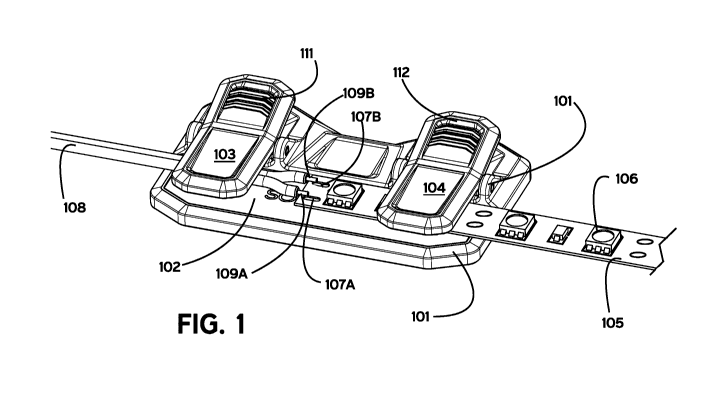
Fig. 'I. Fig. 1 depicts the device of the invention in use, with wires and LED
tape
clamped to the soldering surface.
Fig. 2. Fig. 2 depicts an exploded view of an exemplary device of the
invention.
Fig. 3A and 3B. Fig. 3A depicts a side view of a device of the invention
wherein the
clamp is open to accept a wire. Fig. 38 depicts the device wherein the clamp
is
closed, holding the wire in place on the soldering surface.
Fig. 4. Fig. 4 depicts a top view of the device with LED tape and wire held in
place
by the clamps.
Fig. 5. Fig. 5 depicts a soldering block wherein the fixation elements
comprise a pair
of flexible bands.
Fig. 6. Fig. 6 depicts a soldering block wherein the fixation elements
comprise a pair
of tension clips.
Detailed Description of the Invention.
2
CA 03123200 2021-06-11
WO 2020/123626
PCT/US2019/065680
In a general embodiment, the device of the invention comprises a soldering
block, comprising a substantially planar surface; a first fixation element for
holding a
first electrical elements (or group of elements) to the planar surface; and a
second
fixation means for holding a second electrical element (or group of electrical
elements) to the planar surface, such that end(s) of the first electrical
element(s) and
end(s) of the second electrical element(s) is/are held in proximity to each
other.
An exemplary embodiment of the invention is depicted in Fig. 1, Fig. 2, Fig.
3A and 38, and Fig. 4. It will be understood that these depictions are
exemplary in
nature and that the scope of the invention is not limited to the depicted
embodiments, but extends to any device or method embodying the inventive
concepts described herein.
Base. A first element of the device is the base 101. The base will be an
object such as a block, a plate, or other body comprising a top, planar
surface. For
example, the base may comprise a substantially rectangular body as depicted in
Fig.
1. The base will comprise at least one substantially flat surface, being the
planar
surface on which electrical elements are held in place and soldered or
otherwise
connected together.
The base may comprise any material, such as plastic or other polymeric
material. Exemplary plastics include, for example, polyethylene terephthalate
(PET
or PETE or Polyester), high-density polyethylene (HDPE), polyvinyl chloride
(PVC),
low-density polyethylene (LDPE), polypropylene, polystyrene, or nylon. In
other
implementations, the base may be made of a metal such as steel or aluminum,
wood, ceramic, glass, or other materials, for example, non-conductive
materials. The
base may be manufactured by methods known in the art, such as injection
molding,
additive manufacturing, or milling.
The body will comprise a working surface, for example, a top surface which is
substantially planar.
In one implementation, the top surface comprises a second body, referred to
herein as a plate, that is adhered to top surface of the body or inlaid in
recessed area
of the base to create a working surface. In one embodiment, the body comprises
a
3
CA 03123200 2021-06-11
WO 2020/123626
PCT/US2019/065680
recessed area or channel in which the plate, comprising a planar body is
inlaid. For
example, an assembly of the device is depicted in Fig. 2 with plate element
204
fitting into the base 201, optionally with the use of magnets 205.
The plate may comprise a different material than the material of the body, for
example, being a heat-resistant material that will not melt or burn when
exposed to
hot solder. The plate may comprise a material that is non-stick, which is
resistant to
bonding with hot solder. Exemplary materials for the plate include metal,
ceramic
material, glass material, or organic material. In various embodiments the
plate
comprises a metal, such as aluminum, stainless steel, titanium, or other
metals. In
one embodiment, the plate comprises an organic material such as cork or wood.
The plate acts as a working surface for the soldering of elements and also
acts to
dissipate heat in order to facilitate faster cooling of solder beads. In one
embodiment, a single plate is used. In alternative embodiments, two or more
plates
are laid side by side to create the working surface.
In alternative embodiments, the plate is omitted and the work surface
comprises a material that is painted, coated, or otherwise applied to the top
surface
of the body to provide a working surface for soldering.
In one embodiment, the base and/or the plate comprise grooves for wires or
LED tape strip to sit in.
Fixation Elements. The body will comprise two or more fixation elements for
temporarily holding the LED tape and wires in place in on the top surface of
the
base, e.g. the work area defined by a plate. A fixation element will comprise
any
structure that may apply force to an electrical element (e.g. wire or LED tape
strip)
such that it is held, pressed, or otherwise fixed against the working surface
of the
4
CA 03123200 2021-06-11
WO 2020/123626
PCT/US2019/065680
base or plate. Exemplary fixation elements include clips, clamps, hinged
elements,
or other structures that can be pressed down onto the electrical elements, or
which
the electrical elements can be slipped under. In a primary embodiment, the
fixation
elements comprise tensioned elements that are lifted to insert electrical
elements
and then lowered onto the electrical elements to hold them in place. For
example, in
the exemplary embodiment depicted in Fig. 1, the fixation element comprise
hinged
spring clamps 103 and 104 that can be raised by a user depressing levers 111
and
112.
Fig. 3A and Fig. 3B depict an exemplary fixation element of the invention
comprising a spring tensioned spring clamp 103. Fig. 3A depicts the spring
clamp in
an open position, wherein downward force 114 is applied by the user, for
example,
by finger pressure, to the lever portion 111 of the spring clamp, such that
the clamp
is opened to receive an electrical element 108. In some implementations of the
invention, the spring clamp comprises a plurality of teeth 113 or other
protrusions
that assist in holding the electrical element firmly on the plate 102, if
present, or the
top surface of the base 101. Fig. 3B depicts the spring clamp in the closed
position,
wherein the downward force on the lever portion 111 of the clamp has been
removed
and the spring tensioned clamp returns to a closed position wherein the
electrical
element 108 is held firmly between the plate 102 and the clamp 103, for
example,
with the assistance of teeth 113 on the clamping element.
In alternative embodiments, the fixation elements comprise other structures
for
holding LED tape and wires in place. For example, in one embodiment, the
fixation
elements comprise bands or straps, such as elastic bands, under which the
electrical
elements are slipped and which snugly press the electrical elements to the
working
surface or plate. The bands may comprise any flexible material, for example,
rubber,
woven materials (e.g. woven nylon or polyester) or organic material such as
leather.
For example, as in the embodiment depicted in Fig. 5, the body 501 comprises a
top
surface 502 onto which electrical elements can be held in place by a pair of
bands
503 and 504. Each band may be secured over the electrical element by a
fastener
element located at the terminal end of the band 505 and 506 and complementary
fastener elements on the base. The fastener elements may comprise a snap, a
hole
and peg, or patches of hook and loop material (e.g. VELCRO(TM)). In another
CA 03123200 2021-06-11
WO 2020/123626
PCT/US2019/065680
embodiment, the structure comprises a hinged plate or bar that is lowered onto
the
elements to be soldered and then held in place by a clip, screw, or latch.
Alternatively, in one embodiment, the fixation elements comprise a pair of
tensioned
clips composed of springy, elastic, or supple metal, plastic, or other
material, wherein
electrical elements can be slipped under the clips to hold them in place
against the
working surface or plate. For example, as in the embodiment depicted in Fig.
6, the
body 601 comprises a top surface 602 onto which electrical elements can be
held in
place by a pair of tension clips 603 and 604.
In a primary embodiment, the device comprises two fixation elements, for
example, a left and a right hand element, one of which will hold wires and one
of
which will hold the LED tape. In one embodiment, the fixation elements are
substantially identical, for example, twin alligator clamps as depicted in
Fig. 1. In an
alternative implementation, the fixation elements are not identical, for
example, they
may comprise a first fixation element configured to receive wire and a second
element configured to receive LED tape. In alternative embodiments, three or
more
fixation elements are used.
Uses of the Device. The purpose of the device of the invention is to
facilitate the
connection of two electrical elements, for example, a first electrical element
and a
second electrical element. On one side of the device, the first electrical
element is
held by the first fixation element. In one implementation, the first
electrical element
comprise one or more separate wires (e.g. 1, 2, 3, or 4 wires) or a
multistrand wire.
A multistrand wire, as known in the art comprises multiple individual wires
connected
together or sharing a common outer jacket or insulation layer, for example, a
multistrand wire comprising two, three, four, or more individual wires. In one
embodiment, a multistrand wire comprises a multiple strand wire (e.g. in an
outer
cable housing) at the terminal end of which (e.g. the 1-10 mm end portion of
which),
the individual wires have been separated (or stripped of the outer jacket) and
which
are individually stripped at their tips, for example, stripped at the terminal
0.5 mm, 1
mm, 2 mm, 3 mm, 4 mm, 5 mm, or more to create bare metal wire sections or
contact points suitable for soldering or other connections. These wire ends
may are
splayed to prevent their contacting each other and to align them with the
terminal
positions on the LED tape strip to which they are to be connected. In the case
of
6
CA 03123200 2021-06-11
WO 2020/123626
PCT/US2019/065680
one wire or two or more separate wires, the terminal tips of each are
stripped, for
example, at the terminal 0.5 mm, 1 mm, 2 mm, 3 mm, 4 mm, 5 mm, or more, to
expose bare metal wire sections or contact points suitable for soldering or
other
connection. When held in place by the device of the invention, the wire tips
of the
one or more wires or multistrand wires can be positioned in contact with, or
in close
proximity with the appropriate terminal (proximity being a distance that is
suitable for
soldering, for example by a soldering gun, for example, 0.5 mm or less, 1 mm
or
less, 2 mm or less, 3 mm or less, etc).
On the other side of the device held by the second fixation element is a
second electrical element. In one embodiment, the second electrical element or
component is one or more wires or a multistrand wire, for example, to be
connected
to complementary wires on the other side. In one embodiment, the second
electrical
element is a device, for example a device comprising contacts or terminals,
for
example a circuit board, integrated circuit, or other electronic component. In
a
primary embodiment, the second electrical element is an LED tape strip, e.g.
the
terminal or cut end of an LED tape strip.
As used herein, "LED tape" of "LED tape strip" refers to LED strip lights, as
known in the art. These devices comprise a series of light emitting diodes
(LEDs),
which are typically connected to a driver or controller comprising a power
source and
control elements. Typical driver voltages are 12 V, 24 V, or in the case of
USB-
driven tapes, 5 V. The tape is available in various widths, for example 2 mm,
5 mm,
or 8 mm. The tapes are typically sold in long lengths (e.g. 10 5 meters), and
typically
comprise a 2 pairs of closely spaced terminal, i.e. electrically conductive
leads, at
regular intervals. The tape can be cut between the pairs of leads, resulting
in a free
end that can be connected to the driver or power source. The cut end of the
LED
tape strip will typically comprise two or three terminals.
In the case of connecting one or more wires to LED tape strip, the wires will
be matched to the appropriate LED terminals (for example, any of: ground wire
to
ground terminal; hot wire to hot terminal; neutral wire to neutral terminal;
negative
wire to negative terminal; positive wire to positive terminal; and control
wire to control
terminal). As the wires are pliant, they may be positioned by use of fingers,
pliers, or
7
CA 03123200 2021-06-11
WO 2020/123626
PCT/US2019/065680
other tools to position their ends in contact with or in proximity to their
appropriate
terminal.
The LED tape strip is held in place using the soldering block of the invention
to facilitate connection with one or more wires, wherein each of the one or
more
wires is connected to the appropriate terminal of the LED tape (e.g. hot wire
to hot
terminal, control wire to control terminal, ground wire to ground terminal,
etc.). The
one or more wires may comprise a multistrand wire, for exampleõ wherein at the
end of the multistrand wire, the individual wires are separated and stripped
such that
a length of bare metal wire is exposed for each wire of the multistrand wire.
The scope of the invention encompasses methods of using the devices
described herein for the soldering of electrical components. An exemplary use
of
the device is depicted in Fig. 1 and Fig. 4. In this depiction, an LED tape
strip 105,
comprising a plurality of LEDs 106, is held in place on the base of the device
101 by
the right hand clamp 104. The cut end of the LED tape strip is positioned such
that
the terminals of the strip 107A and 107B are present on the work surface
comprising
a plate 102. One or more wires 108 are held in place by the left side clamp
103.
The ends of the stripped, conducing metal of each wire 109A and 109B is held
in
place by a fixation element on the work surface or plate, with each wire end
in
contact with, or in close proximity (e.g. at a distance of about 3 mm, about 2
mm,
about 1 mm, or less than 1 mm, to its appropriate terminal 107A and 107B on
the
LED tape strip. With the elements conveniently held in place, a user may apply
solder by the use of any soldering tool, such as a standard soldering gun. Any
type
of solder may be used in the device of the invention, for example lead solder,
lead-tin
solder, lead-free solder, and solder comprising flux cores. Upon application
of the
solder and short cooling period during which time the solder hardens, the
fixation
elements, for example, alligator clamps may be engaged (e.g. lifted in the
case of
spring clamps) to release the now-connected LED tape and wires.
It will be understood that the use of the soldering block described herein is
not
limited to the soldering or the soldering of LED tape strip. The device of the
invention may be utilized to hold in place any components which are to be
joined.
Exemplary components include wires being soldered to other wires, wires being
8
CA 03123200 2021-06-11
WO 2020/123626
PCT/US2019/065680
soldered to integrated circuit chips, or any other components, e.g. electrical
components. Likewise, the devices of the invention may be used to join
components
by any means, including soldering, gluing, welding, or other contexts wherein
it is
useful to hold components in place for joining.
Exemplary Embodiments. The device of the invention may be configured in
various ways that encompass the use of two or more fixation elements to hold
electrical elements in place for connection, for example by soldering. An
exemplary
embodiment of the invention is depicted in Fig. 1. An exploded view of the
device of
Fig. 1 is shown in Fig. 2. In this implementation, the device comprises a base
201.
The base comprises a recessed area 208 configured to receive a plate 204.
Optionally, the plate may comprise metal and may be held in place in the base
by
one or more magnets 205. In other implementations, the magnets are omitted and
the plate sits in the recessed area 208 by gravity, adhesives, or
complementary snap
connection elements on the base and plate. The base may comprise elements 209
for affixing the fixation elements to the base, for example, a pair of
knuckles 209 or
like structures that receive pins 205, wherein the pins traverse knuckles 210
on the
clamps 202. The clamps are tensioned by springs 203. As depicted in Fig. 3A
and
3B, the clamps may optionally comprise teeth 113. As depicted in Fig. 2, the
base
may comprise feet, or pads 207 on the bottom surface to prevent slippage of
the
device in the work area.
In one embodiment, scope of the invention encompasses a soldering block,
the soldering block comprising: a substantially planar top surface; a first
fixation
element for holding one or more electrical elements to the planar surface; and
a
second fixation element for holding one or more electrical elements to the
planar
surface. In one embodiment, the first and second fixation elements comprise
tensioned elements that sandwich the one or more electrical elements to the
planar
top surface. In one embodiment, the tensioned elements comprise spring clamps.
In one embodiment, the spring clamps comprise a plurality of teeth. In one
embodiment, the top surface of the soldering block comprises a plate, in one
embodiment, the plate being inlaid in a depression or recessed area of the top
surface of the soldering block. In one embodiment, the plate comprises metal,
ceramic, glass, or organic material. In various embodiments, the plate
comprises
9
CA 03123200 2021-06-11
WO 2020/123626
PCT/US2019/065680
aluminum, stainless steel, cork, or wood.
In one aspect, the scope of the invention encompasses a method of securing
a first electrical element in proximity or in contact with a second electrical
element,
for facilitating connecting them together (in one embodiment the connection of
LED
tape strip to wires), the method comprising the steps of: utilizing a
soldering block,
wherein the soldering block comprises: a substantially planar top surface; a
first
fixation element for holding one or more electrical elements to the planar
surface;
and a second fixation element for holding one or more electrical elements to
the
planar surface; wherein, in one embodiment, the first and second fixation
elements
comprise tensioned elements that sandwich the one or more electrical elements
to
the planar top surface; wherein, in one embodiment, the tensioned elements
comprise spring clamps; wherein, in one embodiment, the spring clamps comprise
a
plurality of teeth; wherein, in one embodiment, the top surface of the
soldering block
comprises a plate, wherein, in one embodiment, the plate is inlaid in a
depression or
recessed area of the top surface of the soldering block; wherein, in one
embodiment,
the plate comprises metal, ceramic, glass, or organic material, wherein, in
various
embodiments, the plate comprises aluminum, stainless steel, cork, or wood; the
method comprising the step of: securing the first electrical element to the
top surface
of the soldering block by the first fixation element; securing the second
electrical
element to the top surface of the soldering block by the second fixation
element; and
wherein the end of the first electrical element and the end of the second
electrical
element are in sufficient proximity or contact to facilitate a connection. In
one
embodiment, the first electrical element comprises one or more wires, for
example
one, two, three or four separate wires, or a multistrand wire. In one
embodiment, the
first electrical element comprises a multistrand wire, for example a
multistrand wire
at which end portion (for example, the end portion being the terminal 2 mm, 3,
mm, 4
mm, 5 mm, 6 mm, 7 mm, 8 mm, 9 mm, or 1 cm of the multistrand) the individual
wires have been separated, and at their tips (for example, the terminal 1 mm,
2 mm,
3 mm, 4 mm, 5 mm, or more) have been stripped of insulation to expose bare
sections of wire or contact points suitable for soldering); for example, a
plurality of
wires or a multistrand wire comprising a negative wire, a positive wire, and
optionally, a ground wire and/or control wire, or the multistrand wire
comprising a hot
wire and a neutral wire, and optionally, a ground wire and/or control wire,
wherein
CA 03123200 2021-06-11
WO 2020/123626
PCT/US2019/065680
the end of each wire of the the multistrand wire has separated and the tips of
each
wire have been stripped such that a length of bare metal wire or contact point
is
exposed. In one embodiment, the first electrical element comprises one or more
separate wires, wherein the end of each of the one or more wires is stripped
such
that a length of bare metal wire is exposed. In one embodiment, the second
electrical element comprises an LED tape strip, wherein the end of the LED
tape
strip comprises one or more terminals or contact points for connection of
wires. In
one embodiment, each of the exposed metal ends of the one or more wires of the
first electrical element are aligned over one of the one or more terminals of
the LED
tape strip in contact or in such proximity that a soldering connection is
readily
achieved by application of a solder bead. In one embodiment, each wire and
terminal is connected by soldering. In one embodiment, each wire and terminal
is
connected by gluing, welding, or splicing.
All patents, patent applications, and publications cited in this specification
are
herein incorporated by reference to the same extent as if each independent
patent
application, or publication was specifically and individually indicated to be
incorporated by reference. The disclosed embodiments are presented for
purposes
of illustration and not limitation. While the invention has been described
with
reference to the described embodiments thereof, it will be appreciated by
those of
skill in the art that modifications can be made to the structure and elements
of the
invention without departing from the spirit and scope of the invention as a
whole.
11