Note: Descriptions are shown in the official language in which they were submitted.
CA 03123642 2021-06-15
WO 2021/045958
PCT/US2020/048248
PCB INTERCONNECT SCHEME FOR CO-PLANAR LED STRIPS
INCORPORATED BY REFERENCE
[0001] A PCT Request Form is filed concurrently with this specification as
part of the
present application. Each application that the present application claims
benefit of or
priority to as identified in the concurrently filed PCT Request Form is
incorporated by
reference herein in its entirety and for all purposes.
BACKGROUND
[0002] Light-emitting diodes (LEDs) may be used as part of an assembly to
provide lighting
and illumination effects in a device. LEDs may be placed upon printed circuit
boards (PCBs)
and connected together. In some applications, multiple LED-containing PCBs may
be used
and may be electrically connected together end-to-end.
SUMMARY
[0003] The present disclosure provides new techniques and apparatuses for
improving the
design and construction of interconnect assemblies between LED boards.
[0004] Details of one or more implementations of the subject matter described
in this
specification are set forth in the accompanying drawings and the description
below. Other
features, aspects, and advantages will become apparent from the description,
the drawings,
and the claims. The following, non-limiting implementations are considered
part of the
disclosure; other implementations will be evident from the entirety of this
disclosure and
the accompanying drawings as well.
[0005] In some implementations, a light-emitting diode (LED) lighting strip
assembly
may be provided that includes a first LED board, a second LED board, and an
interconnect
board. The first LED board may include a first printed circuit board (PCB)
substrate with a
first side and a second side opposite the first side of the first PCB
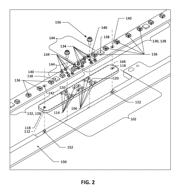
substrate, a plurality of
LEDs located on the first side of the first PCB substrate, where each LED
emits light away
from the first side of the first LED board, an end portion, and a plurality of
compressible
electrically conductive members that each extend outward from the second side
of the first
PCB substrate. Similarly, the second LED board may include a second PCB
substrate with
a first side and a second side opposite the first side of the second PCB
substrate, a plurality
of LEDs located on the first side of the second PCB substrate, where each LED
emits light
away from the first side of the second LED board, an end portion, and a
plurality of
1
CA 03123642 2021-06-15
WO 2021/045958
PCT/US2020/048248
compressible electrically conductive members that each extend outward from the
second
side of the second PCB substrate. The interconnect board may include a third
PCB substrate
having a first region and a second region. The third PCB substrate may include
a plurality
of first electrically conductive pads located on a first side of the third PCB
substrate and
within the first region of the third PCB substrate, and a plurality of second
electrically
conductive pads located on the first side of the third PCB substrate and
within the second
region of the third PCB substrate; each first electrically conductive pad may
be electrically
connected with at least one of the second electrically conductive pads by an
electrically
conductive trace of the interconnect board. In such implementations, the end
portion of the
first LED board may be proximate to the end portion of the second LED board,
the first side
of the third PCB substrate may face the second side of the first LED board and
the second
side of the second LED board, each compressible electrically conductive member
of the first
LED board may be in electrically conductive contact with a corresponding one
of the first
electrically conductive pads, each compressible electrically conductive member
of the
second LED board may be in electrically conductive contact with a
corresponding one of
the plurality of second electrically conductive pads, and a height of the LED
lighting strip
assembly, when each compressible electrically conductive member of the first
LED board
is pressed into electrically conductive contact with the corresponding one of
the first
electrically conductive pads and each compressible electrically conductive
member of the
second LED board is pressed into electrically conductive contact with the
corresponding
one of the second electrically conductive pads, may be substantially equal to
about a sum
of: a thickness of the third PCB substrate of the interconnect board, and the
greater of the
height of the first LED board and the height of the second LED board.
[0006] In some implementations, the compressible electrically conductive
members may
be pogo pins, and each electrically conductive pad of the plurality of first
electrically
conductive pads and the plurality of second electrically conductive pads may
be at least
larger in area than a cross-sectional area of a plunger of a corresponding
pogo pin in the
plane of the second side of the LED board in which the pogo pin is mounted.
[0007] In any of the foregoing implementations, each of the compressible
electrically
conductive members may extend at least about 0.9 mm from the second side of
either the
first LED board or the second LED board.
[0008] In any of the foregoing implementations, the assembly may further
include at least
one first hole located in the first region of the third PCB substrate of the
interconnect board,
2
CA 03123642 2021-06-15
WO 2021/045958
PCT/US2020/048248
at least one second hole located in the second region of the third PCB
substrate of the
interconnect board, at least one hole located in the first LED board and
aligned with the at
least one hole located in the first region of the third PCB substrate of the
interconnect board,
and at least one hole located in the second LED board and aligned with the at
least one hole
located in the second region of the third PCB substrate of the interconnect
board.
[0009] In any of the foregoing implementations, the height of the LED lighting
strip
assembly may be less than about 5.5 mm.
[0010] In any of the foregoing implementations, each compressible electrically
conductive member may be a spring-loaded pin.
[0011] In any of the foregoing implementations, a width of the end portion of
the first
LED board and a width of the end portion of the second LED board may be both
be less
than about 12 mm.
[0012] In any of the foregoing implementations, the LEDs in each plurality of
LEDs may
be spaced less than or equal to about 12 mm apart center-to-center.
[0013] In some implementations, a printed circuit board (PCB) interconnect
assembly
may be provided that includes a first board having a first PCB substrate with
a first side and
a second side opposite the first side of the first PCB substrate, and a
plurality of
compressible electrically conductive members that each extend outward from the
second
side of the first PCB substrate. The assembly may also include a second board
having a
second PCB substrate with a first side and a second side opposite the first
side of the second
PCB substrate, and a plurality of compressible electrically conductive members
that each
extend outward from the second side of the second PCB substrate. The assembly
may further
include an interconnect board that includes a third PCB substrate having a
first region and
a second region, the third PCB substrate including a plurality of first
electrically conductive
pads located on a first side of the third PCB substrate and within the first
region of the third
PCB substrate, and a plurality of second electrically conductive pads located
on the first
side of the third PCB substrate and within the second region of the third PCB
substrate; each
first electrically conductive pad may be electrically connected with at least
one of the second
electrically conductive pads by an electrically conductive trace of the
interconnect board. In
such implementations, each compressible electrically conductive member of the
first board
may be in electrically conductive contact with a corresponding one of the
first electrically
conductive pads, each compressible electrically conductive member of the
second board
3
CA 03123642 2021-06-15
WO 2021/045958
PCT/US2020/048248
may be in electrically conductive contact with a corresponding one of the
plurality of second
electrically conductive pads, and a height of the PCB interconnect assembly
is, when each
compressible electrically conductive member of the first board is pressed into
electrically
conductive contact with the corresponding one of the first electrically
conductive pads and
each compressible electrically conductive member of the second board is
pressed into
electrically conductive contact with the corresponding one of the second
electrically
conductive pads, substantially equal to about a sum of: a thickness of the
third PCB substrate
of the interconnect board, and the greater of the height of the first LED
board and the height
of the second LED board.
[0014] In some such implementations, the compressible electrically conductive
members
may be pogo pins, and each electrically conductive pad of the plurality of
first electrically
conductive pads and the plurality of second electrically conductive pads may
be at least
larger in area than a cross-sectional area of a plunger of a corresponding
pogo pin in the
plane of the second side of the board in which the pogo pin is mounted.
[0015] In any of the foregoing implementations, each of the compressible
electrically
conductive members may extend at least about 0.9 mm from the second side of
either the
first board or the second board.
[0016] In any of the foregoing implementations, the assembly may further
include at least
one first hole located in the first region of the third PCB substrate of the
interconnect board,
at least one second hole located in the second region of the third PCB
substrate of the
interconnect board, at least one hole located in the first board and aligned
with the at least
one hole located in the first region of the third PCB substrate of the
interconnect board, and
at least one hole located in the second board and aligned with the at least
one hole located
in the second region of the third PCB substrate of the interconnect board.
[0017] In any of the foregoing implementations, the height of the PCB
interconnect
assembly may be less than about 5.5 mm.
[0018] In any of the foregoing implementations, each compressible electrically
conductive member may be a spring-loaded pin.
[0019] In any of the foregoing implementations, a width of the first board and
a width of
.. the second board may both be less than about 12 mm.
[0020] In some implementations, a method of assembling an LED lighting strip
assembly
is provided. The method may include placing an interconnect board having a
first printed
4
CA 03123642 2021-06-15
WO 2021/045958
PCT/US2020/048248
circuit board (PCB) substrate onto a supporting structure; the first PCB
substrate may have
a first electrically conductive pads located on a first side of the first PCB
substrate within a
first region of the first PCB substrate and a second electrically conductive
pads located on
the first side of the first PCB substrate within a second region of the first
PCB substrate, and
the first electrically conductive pad may be electrically connected with the
second
electrically conductive pad by an electrically conductive trace of the
interconnect board.
The method may further include placing a first LED board having a second PCB
substrate
with one or more LEDs located on a first side thereof such that a second side
of the second
PCB substrate opposite the first side of the second PCB substrate is proximate
to the first
side of the first PCB substrate of the interconnect board and such that a
first compressible
electrically conductive member extending outward from the second side of the
first LED
board is in electrically conductive contact with the first electrically
conductive pad, placing
a second LED board having a third PCB substrate with one or more LEDs located
on a first
side thereof such that a second side of the third PCB substrate opposite the
first side of the
third PCB substrate is proximate to the first side of the first PCB substrate
and such that a
second compressible electrically conductive member extending outward from the
second
side of the second LED board is in electrically conductive contact with the
second
electrically conductive pad, and applying one or more compressive forces to
the first LED
board and the second LED board to mechanically couple the first LED board and
the second
LED board to at least one of the interconnect board or a support structure.
[0021] In some implementations of the method, the first compressible
electrically
conductive member and second compressible electrically conductive member are
pogo pins,
and each electrically conductive pad of the first electrically conductive pad
and the second
electrically conductive pad are at least larger in area than a cross-sectional
area of a plunger
of a corresponding pogo pin in the plane of the second side of the LED board
in which the
pogo pin is mounted.
[0022] In any of the foregoing implementations of the method, the first
compressible
electrically conductive member and the second compressible electrically
conductive
member extend at least about 0.9 mm from the second side of either the first
LED board or
the second LED board. In any of the foregoing implementations of the method,
the one or
more LEDs of the first LED board and the one or more LEDs of the second LED
board are
spaced less than or equal to about 12 mm apart center-to-center. In any of the
foregoing
implementations of the method, a height of the LED lighting strip assembly may
be, when
5
CA 03123642 2021-06-15
WO 2021/045958
PCT/US2020/048248
the first compressible electrically conductive member of the first LED board
is in
electrically conductive contact with the first electrically conductive pad and
the second
compressible electrically conductive member of the second LED board is in
electrically
conductive contact with the second electrically conductive pad, substantially
equal to about
a sum of: a thickness of the first PCB substrate of the interconnect board,
and the greater of
the height of the first LED board and the height of the second LED board.
[0023] It should be appreciated that all combinations of the foregoing
concepts and
additional concepts discussed in greater detail below (provided such concepts
are not
mutually inconsistent) are contemplated as being part of the subject matter
disclosed herein
and/or may be combined to achieve the particular benefits of a particular
aspect. In
particular, all combinations of claimed subject matter appearing at the end of
this disclosure
are contemplated as being part of the subject matter disclosed herein.
[0024] These and other features of the disclosed embodiments will be described
in detail
below with reference to the associated drawings.
BRIEF DESCRIPTION OF DRAWINGS
[0025] The various implementations disclosed herein are illustrated by way of
example, and
not by way of limitation, in the figures of the accompanying drawings, in
which like
reference numerals refer to similar elements.
[0026] Figure 1 presents an exploded view of part of an illuminable assembly
as described
herein.
[0027] Figure 2 presents an exploded view of an interconnect assembly as
described
herein.
[0028] Figure 3 presents a view of an interconnect board used in an
interconnect assembly
as described herein.
[0029] Figure 4 presents an assembled view of part of an illuminable assembly
as
described herein.
[0030] Figure 5 presents an assembled view of interconnected LED boards.
[0031] Figure 6 presents a view of one side of a curved LED board.
[0032] Figure 7 presents a view of a different side of a curved LED board.
[0033] Figure 8 presents a view of an illuminable assembly as described
herein.
6
CA 03123642 2021-06-15
WO 2021/045958
PCT/US2020/048248
[0034] Figure 9 presents a view of a compressible electrically conductive
member.
[0035] Figures 1 through 7 and 9 are to-scale within each Figure, although the
scale may
vary Figure to Figure.
DETAILED DESCRIPTION
[0036] In the following description, numerous specific details are set forth
to provide a
thorough understanding of the presented embodiments. Embodiments disclosed
herein may
be practiced without some or all of these specific details. In other
instances, well-known
process operations have not been described in detail to not unnecessarily
obscure the
disclosed embodiments. Further, while the disclosed embodiments will be
described in
conjunction with specific embodiments, it will be understood that the specific
embodiments
are not intended to limit the disclosed embodiments.
[0037] This disclosure relates to a light bar interconnect scheme. Multiple
straight or
curved, long, narrow rigid printed circuit boards with linear arrays of LEDs
(referred to
below as "LED boards") on them may be used as part of an illuminable assembly
and
electrically connected to each other end-to-end. Such LED boards may be used
to provide
edge lighting, e.g., of a surface adjacent and perpendicular to the LED
boards, or of a
translucent light diffusion element.
[0038] To improve the visual aesthetic and uniformity of the illumination
provided by the
LEDs, all of the LEDs may be coplanar. The LED board assembly may also have a
low
profile, e.g., less than 7 mm, or less than about 5.5 mm, total height in a
direction
perpendicular to the board and less than 1 1 mm total width along one
dimension. Such a
small profile LED board assembly may be beneficial for usage in thin or low
profile
illumination assemblies to reduce the space claim of the assembly and/or
reduce the
appearance of a frame/seam of the illumination assembly. Such LED board
assemblies may
be manufactured as a single, contiguous PCB, but the cost of doing so may be
uneconomical
for larger-sized LED boards that follow convoluted paths, e.g., a U-shaped PCB
strip that is
2 feet on a side and has a width of 1 cm might use a 2 foot square sheet of
PCB material in
order to be fabricated as a single piece-99% of this material may, in some
cases, be cut
away to provide the finished part. An LED board assembly may thus be composed
of smaller
PCB boards that may be joined end-to-end to provide the desired end PCB
layout. This
allows for more efficient manufacturing, easier repairs, and more compact
shipping.
[0039] Various commercial-off-the-shelf (COTS) connectors and other connection
7
CA 03123642 2021-06-15
WO 2021/045958
PCT/US2020/048248
schemes were considered for the inter-LED board connections, but none of them
provided
the preferred tolerance allowances, current capacity, compactness, and ease-of-
assembly
desired. A new interconnect between each pair of adjacent LED boards was
designed to
satisfy these aspects.
[0040] Various implementations of an interconnect assembly for LED lighting
strips are
discussed herein. Each assembly includes an interconnect and two LED boards.
The
interconnect includes a single interconnect board, i.e., a printed circuit
board, that fits
underneath adjacent LED boards, i.e., on the side of the LED boards opposite
the side where
the LEDs are mounted, and provides electrical connection therebetween by way
of exposed
electrical contact pads that face towards the LED boards. The interconnect
also uses a
plurality of compressible electrically conductive members, e.g., spring-loaded
pins or spring
connectors, to connect the LED boards with the electrical contact pads of the
interconnect
board. In some implementations, the spring-loaded pins are sized so as to not
interfere with
the light emitted from the LEDs and to fit within the desired vertical height
profile. The
LED boards and the interconnect board may be fastened using aligned holes in
each board,
such that a fastener can be used to couple the LED board and interconnect
board to a
supporting structure, e.g., a housing, frame or other rigid component.
Furthermore, the
interconnect can be designed to carry large currents, i.e. greater than 4
amps, through
providing multiple compressible electrically conductive members that are
electrically
connected with one another within the LED board and corresponding electrical
contact pads
that are electrically connected with one another within the interconnect
board.
[0041] Such interconnect assemblies provide improved ease of manufacture and
assembly, as well as replacement of parts, since the interconnects may be
established
through simply stacking the LED boards on top of the interconnect board. Such
interconnects may allow for minimal LED spacing, i.e. on the order of 12 mm
center-to-
center spacing or less, without causing any lighting pattern non-uniformities.
The
interconnect may also handle misalignments in the x, y, and theta-z direction
between the
boards without sacrificing performance.
[0042] Figure 1 presents an exploded view of an example interconnected LED
board
assembly 166 having multiple interconnect assemblies 100 according to some
implementations. As discussed earlier, multiple LED boards 128 may be used as
part of an
illuminable assembly where it would be impractical to manufacture a single PCB
board for
the entire illuminable assembly. In such instances, an interconnect assembly
100 may be
8
CA 03123642 2021-06-15
WO 2021/045958
PCT/US2020/048248
used to connect two adjacent, smaller-sized LED boards 128 using an
interconnect board
102. The interconnect assembly 100 may be fastened to a supporting structure
150.
Fastening the interconnect assembly 100 to the supporting structure 150 may be
beneficial
for providing a defined structure or pattern for the interconnect assembly
100, which may
be rigid, semi-rigid, or flexible. If there are three or more LED boards 128
to connect,
multiple interconnect assemblies 100 may be used. Generally, if there are N
number of LED
boards to be connected together in a chain, N-1 interconnect assemblies may be
used, each
interconnect assembly 100 successively connecting adjacent LED boards 128.
Each
interconnect assembly 100 includes two adjacent LED boards 128 and an
interconnect board
102. For example, Figure 1 shows seven LED boards 128 and six interconnect
boards 102
that form six interconnect assemblies 100.
[0043] Figure 2 presents a close-up, exploded view of an interconnect assembly
100. The
interconnect assembly 100 may include an interconnect board 102, a first LED
board 130
of the LED boards 128, and a second LED board 132 of the LED boards 128. In
some
implementations, an LED board 128 that is the first LED board 130 of one
interconnect
assembly may be the first LED board 130 or the second LED board 132 of a
different
interconnect assembly 100, and vice-versa. The denomination of an LED board
128 as a
first LED board 130 or a second LED board 132 is only for the purpose of
clarity in this
description.
[0044] The first LED board 130 and the second LED board 132 each may have one
and/or
a plurality of LEDs 136 laid out along their length that may be electrically
connected to each
other or to an integrated circuit LED driver 138. In some embodiments the LEDs
136 may
have a spacing of about 12 mm center-to-center. In some implementations, due
to the design
of the interconnect, the same center-to-center spacing may persist across the
junctions
between LED boards 128. In such implementations, for example, an LED 136 on
the first
LED board 130 may be 12 mm center-to-center from the closest LED 136 on the
second
LED board 132. This may be desirable to provide a uniform light distribution
to an outside
observer.
[0045] The first LED board 130 and the second LED board 132 each may also have
one
or more LED drivers 138. In some implementations, the LED drivers 138 may be
omitted
or located remote from the LED boards. Each LED driver 138 may be electrically
connected
with and used to control at least one LED 136. In some implementations, each
LED driver
138 may control four LEDs 136. In other implementations, each LED driver 138
may
9
CA 03123642 2021-06-15
WO 2021/045958
PCT/US2020/048248
control one LED 136, two LEDs 136, three LEDs 136, or more than four LEDs 136.
The
LED driver 138 may be placed on the LED board 128 at a position closest to the
LEDs 136
it controls. In some implementations, if an LED driver 138 controls four
successive LEDs
136 along the LED board 128, it may be placed between the LEDs 136 such that
two of the
LEDs 136 it controls are on either side of the LED driver 138. The placement
of the LED
drivers 138 may be selected so to not interfere with the spacing and light
emission of the
LEDs 136.
[0046] In implementations where the LEDs 136 and LED drivers 138 are
positioned as
described above, the LED boards 128 may have limited space for other
components or
features, such as compressible electrically conductive members or holes. In
some
implementations, this constrains an interconnect assembly between the first
LED board 130
and the second LED board 132. For example, in implementations where the LEDs
136 may
be placed about 12 mm center-to-center, and the LED drivers 138 may be placed
between
every fourth and fifth LED 136, there may be limited space on the LED boards
128 for
compressible electrically conductive members to connect the LED boards 128 and
holes for
fastening the LED boards 128 to a supporting structure.
[0047] One or more spring connectors 134 may be placed at the end portions 144
of the
first LED board 130 and second LED board 132. Spring connectors 134, or
compressible
electrically conductive members, are electrical connectors that are
electrically connected
with the LEDs 136 and/or LED drivers 138, and which may provide for a spring-
loaded
electrical connection that includes an electrical contact that may be movable
along a
direction generally normal to the plane of the LED board 128; the movable
portion of the
electrical connectors may be biased, e.g., with a spring or other resiliently
deformable
component, to cause the movable portion or a resiliently deformable component
itself to be
urged towards, for example, the interconnect board 102. Although the present
implementation is described in reference to LEDs 136 and/or LED drivers 138
for the LED
boards 128, such components may be omitted and/or other components may be
implemented
instead, such as transducers, acoustic elements, etc. In some implementations,
spring
connectors 134 may be pogo pins, which are, as the name suggests, electrical
contacts with
a spring-loaded plunger that is able to translate along an axis that is
perpendicular to the
PCB in which such electrical contacts are mounted. Spring connectors 134
generally operate
to electrically connect with first conductive pads 106 or second conductive
pads 114 on the
interconnect board 102.
CA 03123642 2021-06-15
WO 2021/045958
PCT/US2020/048248
[0048] Spring connectors 134 connect with the conductive pads 106, 114 by a
mechanical
force that urges the moveable portion of the spring connectors 134 to the
contact the
conductive pad 106, 114. In some implementations, spring connectors 134 are
advantageous
because a spring or other resiliently deformable component permits a
misalignment between
the interconnect board 102 and one of the LED boards 128 while still
maintaining an
electrical connection therebetween. In some implementations, such
misalignments may
include inexact spacing between the conductive pads of adjacent LED boards (x
direction
misalignment; such as may be caused by variation in the gap between the
adjacent ends of
two LED boards), inexact alignment between the longitudinal center lines of
adjacent LED
boards that may still be parallel (y direction misalignment; such as may be
caused by
transverse offsets between the ends of two LED boards), and inexact alignment
between the
longitudinal center lines of adjacent LED boards, such that they are not
parallel, i.e. angled
with respect to each other (theta-z misalignment).
[0049] The spring connectors and conductive pads may be sized to allow for the
misalignments noted above while maintaining an electrical connection. For
example, in
some implementations, the conductive pads may be sized such that, under any
worst-case
tolerance stack-up conditions for the interconnect assembly, a centerline of a
corresponding
spring connector for each conductive pad may be at least 0.25 mm from the edge
of the
corresponding conductive pad, thereby creating a potential 0.5 mm diameter
contact area
(spring connectors, such as pogo pins, may often have a hemispherical or domed
tip,
resulting in a theoretical "zero" area contact (assuming the tip is a perfect
hemisphere and
the conductive pad a perfect plane), although various factors such as
imperfect machining,
material deformation, etc. typically result in a larger contact area than zero
or such a larger
contact area may be intentional for conductivity purposes). By sizing the
conductive pads
to be 2.5 mm on a side, up to 2 mm of misalignment can be tolerated between
adjacent LED
boards. It will be understood that other dimensional values may be used
instead, depending
on the misalignment tolerances desired, and the above example is merely
provided as one
possible scenario. In some implementations, the conductive pads may be sized
so as inscribe
a circle that is at least 2.75 times larger in diameter than, e.g., 2.75 to 4
times larger than,
for example, the diameter of the plunger of a pogo pin or other spring
connector that is used.
[0050] In some implementations, an interconnect assembly 100 is tolerant of
various
degrees of misalignment. In some implementations, the interconnect assembly
100 may
tolerate a misalignment in an x- and/or y-dimension of less than +-0.5 mm, +-
0.4mm, +-0.3
11
CA 03123642 2021-06-15
WO 2021/045958
PCT/US2020/048248
mm, +-0.2 mm, and/or less than +-0.1 mm. In some implementations, the
interconnect
assembly 100 may tolerate a misalignment in a theta-z dimension of less than
0.1 mm,
and/or less than 0.2 mm.
[0051] In some implementations, a spring connector 134 may extend from the
surface of
the LED board 128 facing the interconnect board 102 at least about 0.9 mm. If
the
interconnect board 102 and the LED board 128 are misaligned so as to cause a
space no
more than 0.2 mm between them at any given position between the two boards
(which may
occur due to rotation of one board with respect to the other or loosening of a
fastener
coupling them together in addition to the above misalignments), a spring
connector 134 may
still maintain electrical contact with its respective conductive pad 106, 114
on the
interconnect board 102. The spring connectors 134 thus increase the tolerances
of the
interconnect assembly 100 and permits increased tolerances for manufacturing
the various
components of the interconnect assembly 100.
[0052] In the implementation described herein, the LED boards 128 are
connected via an
interconnect board 102, which has conductive pads 106, 114 that connect with
the spring
connectors 134 of the first LED board 130 and the second LED board 132. In
some
implementations, the interconnect board 102 includes a first region 104 and a
second region
112, where the first region 104 has a first plurality of conductive pads 106
and the second
region 112 has a second plurality of conductive pads 114. Each conductive pad
of the first
plurality of conductive pads 106 connects with a corresponding one of the
spring connectors
134 of the first LED board 130. Likewise, each conductive pad of the second
plurality of
conductive pads 114 connects with a corresponding one of the spring connectors
134 of the
second LED board 132.
[0053] Each conductive pad of the first plurality of conductive pads 106 is
electrically
connected via a conductive trace of the interconnect board 102 with at least
one of the
conductive pads of the second plurality of conductive pads 114. In other
implementations,
the first plurality of conductive pads 106 and the second plurality of
conductive pads 114
may be a single contiguous conductive pad or other electrically conductive
configuration
that may be beneficial to conduct electricity from one part of the
interconnect board 102 to
another part of the interconnect board 102. Figure 3 presents a view of an
interconnect board
102 showing traces 108. In some implementations, two of the conductive pads of
the first
plurality of conductive pads 106 are connected with two of the conductive pads
of the
second plurality of conductive pads 114. This may be advantageous to increase
the
12
CA 03123642 2021-06-15
WO 2021/045958
PCT/US2020/048248
amperage that may be carried via the traces 108, conductive pads 106, 114, and
spring
connectors 134, which in some implementations may exceed 4 amps. For example,
in some
implementations the spring connectors 134 may not be rated to carry 4 amps, or
are rated
for at least 2 amps and less than 4 amps.
[0054] In such embodiments, using two or more spring connectors 134 in
parallel may
distribute the amperage, allowing for each spring connector 134 to carry less
than 4 amps,
reducing the potential for failure of any spring connector 134. The use of
spring connectors
in parallel in some implementations may also provide redundancy for the
purpose of
improved reliability. The traces between each conductive pad may have
different sizes,
shapes, or materials. In some implementations, traces that are intended to
carry 4 amps (or
larger amperages) will be thicker or wider than traces that will carry less
than 4 amps. In
some implementations traces that will carry large currents, e.g. more than 4
amps, may use
copper planes on one or more layers of the PCB of the interconnect board.
[0055] In the implementation shown, the conductive pads and traces in the
first region
104 and the second region 112 are symmetrical across a line of symmetry
between the first
region 104 and second region 112. However, it should be understood that in
other
implementations the pluralities of conductive pads 106, 114and traces 108 may
not be
symmetrical. The conductive pads 106, 114 and traces 108 may be placed in any
arrangement that allows the interconnect board 102 to electrically connect two
LED boards
128 as described herein.
[0056] In some implementations the interconnect board 102 has a thickness 124
that is
less than 1.6 mm. This may be advantageous to minimize the total thickness of
the
interconnect assembly 100. In some implementations the interconnect board 102
has a width
126 less than 10.5 mm. This may be advantageous to allow the interconnect
board to fit
within an illuminable assembly as described herein.
[0057] Returning to Figure 2, in some implementations each of the conductive
pads 106,
114 is sized to allow for easy connection with spring connectors 134 of the
first and second
LED boards 130, 132. The conductive pads 106, 114 are shown as roughly square
in Figure
2, but may be rectangular, circular, pentagonal, or any other shape that
facilitates an
electrical connection with a spring connector 134 and allows for some amount
of
misalignment between the spring connectors 134 and the conductive pads 106,
114. In some
implementations, the conductive pads 106, 114 may have a diameter (or
equivalent,
13
CA 03123642 2021-06-15
WO 2021/045958
PCT/US2020/048248
perpendicular dimensions) of at least 2.5 mm. This may allow the conductive
pads 106, 114
to maintain electrical connection with the spring connectors 134 of the LED
boards 128
without precise positioning.
[0058] In some implementations, the conductive pads 106, 114 are sized based
on a
tolerance range for manufacturing and positioning the interconnect board 102
and the LED
boards 128, so that the LED boards 128 and the interconnect board 102 can
maintain an
electrical connection between each conductive pad 106, 114 and a corresponding
spring
connector 134 within the tolerance range. In some embodiments, this tolerance
range may
be less than about 1 mm misalignment between the interconnect board 102 and
either of the
first LED board 130 or the second LED board 132 in a direction parallel to the
surface of
the interconnect board 102. In some embodiments, a tip of a spring connector
that contacts
a conductive pad may have a contact area having diameter of about 0.5 mm. In
such
embodiments, a central point of contact of a spring connector 134 may be off-
center from
the center of its respective conductive pad 106, 114 by up to about 1 mm and
still have the
entire contact area of the tip of the spring connector in contact with the
conductive pad 106,
114. In some embodiments, the diameter (or equivalent perpendicular
dimensions) may be
at least about 5 times larger, at least about 4 times larger, at least about 3
times larger, or at
least about 2 times larger than the diameter of the contact area of the spring
connector 134.
For example, if the spring connectors 134 have a contact area diameter of
about 0.5 mm, the
conductive pads 106, 114 may have a diameter of at least 2.5 mm, 2.0 mm, 1.5
mm, or 1.0
mm.
[0059] In some implementations the interconnect board 102 has at least one
fastener hole
120. In some implementations, a fastener hole 120 may be sized to fit around a
boss 154
(not visible in Figure 2) that protrudes from a supporting structure 150 to
which the
interconnect board 102 may be fastened. In some implementations, the fastener
hole 120
may be sized smaller than the boss 154, so that the interconnect board 102
rests on top of
the boss 154 (or, alternatively, the threaded hole for the fastener may simply
be provided in
a feature without using a boss 154). In some implementations there may be a
fastening hole
120 in the first region 104 and in the second region 112, while in other
implementations
there may be only one single fastening hole 120, located in either region 104,
112. In some
implementations there may be no fastening holes 120. In such implementations,
the
interconnect board 102 may be fastened to a supporting structure 150 by a
different
mechanism, such as a clamp that that fits over the LED boards and/or the
interconnect board
14
CA 03123642 2021-06-15
WO 2021/045958
PCT/US2020/048248
102, or by an adhesive.
[0060] In some implementations the interconnect board 102 has at least one
positioning
hole 118. A positioning hole 118 may be smaller than a fastening hole 120, and
may be used
to fit around a peg 152 that protrudes from a support structure 150. The
positioning hole
118 may be sized slightly larger than the peg 152 in order to easily fit
around the peg 152
while minimizing the movement of the interconnect board 102 along a plane
perpendicular
to a central axis of the peg 152. In some implementations there may be a
positioning hole
118 in the first region 104 and in the second region 112, while in other
implementations
there may be only one positioning hole 118, located in either region 104, 112.
In some
implementations there may be no positioning holes 118. In such implementations
the
interconnect board 102 may be properly positioned by a different mechanism,
such as by
recess 158, shown in Figure 1, that the interconnect board 102 fits into,
where the
dimensions of recess 158 and the LED boards 128 positioned above the
interconnect board
102 in the assembled interconnect assembly 100 inhibit the movement of the
interconnect
board 102. In some implementations, the interconnect board 102 is positioned
by an
adhesive.
[0061] Similar to the interconnect board 102, the first LED board 130 and the
second LED
board 132 may also each have at least one positioning hole 142 and/or at least
one fastening
hole 140. The positioning hole 142 of the first or second LED board may fit
around a peg
152 and line up with a positioning hole 118 in the interconnect board 102. In
some
implementations positioning hole 142 may be a different shape, such as a slot,
that has an
opening larger than peg 152 and may therefore fit around peg 152 without
restricting the
movement of the interconnect board 102 in an x- and/or y-direction. While a
fastener hole
120 in the interconnect board 102 may be sized slightly larger than a boss 154
of the
supporting structure 150, a fastening hole 140 in either of the LED boards may
be smaller
than the fastener hole 120. However, in some implementations the fastener hole
120 may be
the same size as a fastening hole 140, such that a boss 154 would not fit
through either hole.
Instead, the fastening holes 118, 140 may be sized to allow the body of a
fastener 156 to
pass therethrough while not allowing the head of the fastener 156 to pass
through.
[0062] In some implementations, the positioning holes 142, fastening holes
140,
positioning hole 118, and fastener hole 120 may be along a longitudinal center
line of each
of the LED boards and interconnect board. In other implementations, one or
more of the
holes may be off the longitudinal center line. Positioning the holes off-
center may allow for
CA 03123642 2021-06-15
WO 2021/045958
PCT/US2020/048248
easier assembly, as there may be only one correct orientation for positioning
the LED boards
and interconnect boards.
[0063] When the interconnect assembly 100 is assembled, the fastener 156 urges
the LED
boards 128 and the interconnect board 102 together, contacting the spring
connectors 134
with the conductive pads 106, 114. Thus, an electrical circuit is formed
between the spring
connectors 134 of the first LED board 130 and the spring connectors 134 of the
second LED
board 132 via the first plurality of conductive pads 106, the second plurality
of conductive
pads 114, and the conductive traces 108 therebetween in the interconnect board
102. In some
embodiments, if the LED boards 128 are misaligned, the spring connectors 134
may
.. maintain an electrical connection due to the spring or other moveable
portion extending
from the spring connector 134 outwards, towards the interconnect board 102 and
due to the
oversized dimensions of the conductive pads 106, 114 on the interconnect board
102. As
each spring connector 134 may be independently urged towards the interconnect
board 102,
a considerable amount of misalignment may be tolerated.
[0064] Returning to Figure 1, the LED boards 128 may be used as part of a LED
lighting
strip assembly or interconnected LED board assembly 166 in an illuminable
assembly that
illuminates a larger apparatus. In some implementations, the illuminable
interconnected
LED board assembly 166 includes a supporting structure 150 that the LED boards
128 and
interconnect boards 102 are fastened to as an interconnect assembly 100. The
supporting
structure 150 may have a recess 158 for each interconnect assembly 100 that is
sized to fit
an interconnect board 102. In some implementations each recess 158 has a depth
about the
same as the thickness 124 of the interconnect board 102, and a width and
length at least the
same as the width and length of the interconnect board 102. This may be
advantageous to
allow the LED boards 128 to be co-planar, as the interconnect board 102 does
not extend
out of the recess 158. As the LED boards 128 are co-planar, the LEDs 136 are
co-planar,
improving the uniformity of the visual effect from the LEDs 136. In some
embodiments,
the interconnect boards may sit on top of the supporting structure 150 with no
recesses 158.
While the present example is described in reference to LEDs 136 and LED boards
128, other
electrical components and boards may be implemented using the interconnect
board 102,
such as acoustic components, MEMs, etc.
[0065] Additionally, each recess 158 may have at least one boss 154 and at
least one peg
152. The pegs 152 may be used to position the interconnect board 102 and LED
boards 128
and facilitate the interconnect assembly 100. The bosses 154 may provide
additional depth
16
CA 03123642 2021-06-15
WO 2021/045958
PCT/US2020/048248
for a fastener. In some embodiments, the depth of the supporting structure 150
below each
recess 158 is insufficient for a fastener to properly catch and thus hold the
interconnect
assembly 100 together. A boss 154 may thus be used to permit a sufficient
depth for a
fastener, while also allowing the recess 158 to have a depth of about the
thickness of the
interconnect board 102.
[0066] The dimensions of the support structure 150 may restrain the possible
dimensions
of the LED lighting strip assembly 166. Thus, in some implementations, the LED
boards
128 are a rigid PCB board having a width less than about 11 mm. Additionally,
in some
implementations the height of the interconnect assembly 100 is less than 7 mm.
This may
be to prevent the interconnect assembly from affecting the light from the LEDs
136, which
may cause noticeable disruption in the light pattern from the LEDs 136 as seen
by an
observer. It may also allow for sufficient material in the supporting
structure 150. As can be
seen in Figure 1, a recess 158 in the supporting structure 150 is sized to fit
an interconnect
board 102. A thicker interconnect arrangement may use a deeper recess/thinner
supporting
structure below the interconnect to maintain co-planarity of the LEDs 136.
This may
increase the chance of failure of the support structure 150 at the recess 158,
increase the
design complexity of the supporting structure 150, and/or decrease the
supporting
structure's 150 rigidity, all of which are undesirable.
[0067] Figure 4 presents an assembled view of the interconnected LED board
assembly
166 shown in Figure 1. Specifically, inset view 460 presents a close-up view
of an
assembled interconnect assembly 100. Interconnect board 102 may be seen
fitting into
recess 158. Two fasteners 156 each fasten a corresponding LED board 128 to the
interconnect board 102 and the supporting structure 150.
[0068] As noted above, in some implementations an interconnect assembly 100
has a total
height that allows for a low profile total height, e.g., less than 7 mm, or
less than about 5.5
mm, in a direction perpendicular to the board. In some implementations, the
height of the
assembled interconnect assembly 100 is substantially equal to a sum of the
thickness 124 of
the interconnect board 102, and the greater of a height of either the first
LED board 130 or
the second LED board 132. Substantially equal, in this context, may include
allowing the
height to be equal to this sum or equal to this sum plus an additional amount,
e.g., less than
0.2 mm or less than 0.1mm, to account for potential small gaps between the
interconnect
board 102 and either the first LED board 130 or the second LED board 132,
e.g., gaps of
less than 0.2 mm, less than 0.1 mm, or no gaps. The height of an LED board
128, as used
17
CA 03123642 2021-06-15
WO 2021/045958
PCT/US2020/048248
herein, is a maximum normal distance between a bottom or second side of the
LED board
128 and a topmost or uppermost surface of the components mounted to the first
side of the
LED board, such as a top surface of an LED 136, a top surface of an LED driver
138, an
upper surface of a compressible electrically conductive member 134, etc.
Notably, in some
implementations the height of an LED board 128 does not include the distance a
compressible electrically conductive member 134 extends from the bottom or
second side
of the LED board 128, as the compressible electrically conductive member 134
may, in
some instances, be compressed into the LED board 128. As discussed further
below in
reference to Figure 9, a compressible electrically conductive member 134 may
be
compressed when an interconnect assembly 100 is assembled, and may not extend
from the
bottom or second side an LED board 128 when compressed.
[0069] Figure 5 presents another view of an interconnected LED board assembly
166, this
view lacking the supporting structure 150.
[0070] Figures 6 and 7 present a front and back view of a curved LED board
129. The
curved LED board 129 includes a PCB 146 having one and/or a plurality of LEDs
136 and/or
LED drivers 138 placed thereon. Curved LED board 129 also has spring
connectors 134, a
positioning hole 142, and a fastening hole 140 at both end portions 144.
[0071] Curved LED board 129 curves within the plane of the PCB board 146. The
LEDs
136 may generally have a higher luminescence per energy spent when emitting
light in a
direction perpendicular to the plane of a surface on which they are mounted,
compared to
emitting light parallel to the plane of a surface on which they are mounted.
Thus, by having
the LED board 129 curve within the plane of the PCB board 146, the LEDs 136
may act
more efficiently to achieve a similar amount of luminescence than if the LED
board 129
curved out of the plane of the PCB board 146. If the LED board 129 curved out
of the plane
of the PCB board 146, such as by using a flexible circuit board, the LEDs 136
would have
to emit light parallel to the surface on which they are mounted, which would
result in
increased energy to achieve a similar luminescence. Furthermore, if the LED
board curved
out of the plane of the PCB board, such as by using a flexible circuit board,
the total height
of the LED board in the direction of the axis of curvature may be greater than
the height of
an embodiment as shown where the LED board curves within the plane of the PCB
board.
Curved LED board 129 may also be straight at each end portion 144 to
facilitate connection
with an interconnect board 102. In some embodiments, both the end portion of
the LED
board 129 and the interconnect board 102 may be curved.
18
CA 03123642 2021-06-15
WO 2021/045958
PCT/US2020/048248
[0072] Figure 7 presents a back view of a curved LED board 129. The
positioning holes
142 and fastening holes 140 are still visible, as are plungers of the spring
connectors 134,
i.e., a portion of the compressible electrically conductive members. The back
side of curved
LED board 129 may not have any other features, and the end portions 144 may
connect with
an interconnect board 102 in order to electrically connect curved LED board
129 with
another LED board 128, 129. In some embodiments, the spring connectors 134 may
extend
from the back of the curved LED board 129 by about 0.9 mm. Additionally, the
spring
connectors may extend from the front of the curved LED board 129 by less than
about 2.2
mm, or about 2.15 mm.
[0073] Figure 8 is a partial view of an illuminable assembly 864 having two
interconnected LED board assemblies 866 as described herein, each having a
first LED
board 830, a second LED board 832, and an interconnect board 802. The LED
boards 830
and 832 may each have a plurality of LEDs 836 and a plurality of compressible
electrically
conductive members 834, as discussed above. Each of the interconnected LED
board
assemblies 166 may be within and hidden by the illuminable assembly 864. One
interconnected LED board assembly 866 is on the bottom of illuminable assembly
864,
having LEDs 836 that emit light upwards, while another interconnected LED
board
assembly is mounted on the top of illuminable assembly 864, having LEDs
836positioned
to emit light downwards. While only one interconnect assembly is shown for the
top and
bottom interconnected LED board assemblies 866, each interconnected LED board
assembly 866 may have multiple interconnect assemblies, as described earlier.
The light
from each LED 836 may then be emitted into a light region 870 between the two
interconnected LED board assemblies, which may, for example, be bounded by a
diffuser
panel or other light-spreading device to form an evenly illuminated wall or
surface.
[0074] Figure 9 is a view of an example compressible electrically conductive
member
134. A compressible electrically conductive member 134, or spring connector
134, may
have three main parts: an internal body portion 184, a plunger 186, and an
external body
portion 182; an internal spring (not visible) is housed within the body
portions 182, 184 and
applies force to the plunger 186 to cause the plunger 186 to be urged out of
the exposed end
of the internal body portion 184. The internal body portion 184 may fit inside
of a PCB
when the compressible electrically conductive member 134 is installed in a
hole in the PCB;
this is in contrast to typical pogo pins, which have housings that often
extend out from both
sides of the PCB in which they are mounted (typical pogo pins are not designed
to allow the
19
CA 03123642 2021-06-15
WO 2021/045958
PCT/US2020/048248
pins to be fully compressed into the PCB). The internal body portion 184
therefore may
have a length, as measured along a central axis normal to a circular cross
section of the
compressible electrically conductive member 134, less than about 1.44 mm, so
that the
internal body portion 184 is no longer than the thickness of a PCB it is
configured to
interface with.
[0075] Plunger 186 extends from the internal body portion 184, and is movable
with
respect to the internal body portion 184 along the central axis. As part of an
interconnect
assembly 100, the plunger 186 of each compressible electrically conductive
member 134 is
in electrically conductive contact with a conductive pad 106, 114 on an
interconnect board
102, compressing the plunger 186 towards the internal body 184. In some
implementations,
plunger 186 may be the only part of the compressible electrically conductive
member 134
that extends beyond the surface of the PCB on the side of an LED board 128
facing the
interconnect board 102.
[0076] The external body portion 182, when installed in an LED board 128, may
extend
from the side of the PCB facing away from the interconnect board 102. The
external body
portion 182 has a flange that may limit the movement of the compressible
electrically
conductive member 134 through the PCB during installation, thereby ensuring
that the
compressible electrically conductive member 134 is installed at the
appropriate height/depth
relative to the PCB. The external body portion 182, inclusive of the flange,
may have a
length less than about 2.2 mm to avoid interfering with the light emitted from
LEDs 136.
[0077] It will be understood that the interconnects shown herein may be
particularly well-
suited for making end-to-end connections between relatively thin, long PCBs,
e.g., such as
may be used for LED strip lighting. Such PCBs can be approximately 1 cm wide
and an
order or magnitude more larger in length. Some LED lighting applications use
at least two
conductive paths to be established across each such end-to-end connection; for
LED lighting
applications in which the color of the LEDs may be controlled, such
connections may use
at least four conductive paths to be established across each such end-to-end
connection¨
power, ground, clock signal, and data signal. Establishing a robust, easy-to-
assemble end-
to-end connection between adjacent LED boards such as those discussed above
may be
problematic. In fact, several alternative options were considered, but the
foregoing
interconnect arrangement had preferable levels of performance.
[0078] For example, one alternative to the foregoing interconnect arrangement
utilizes a
CA 03123642 2021-06-15
WO 2021/045958
PCT/US2020/048248
butt-mounted, 90 pin connector, with a female connector located on an end of
one board,
and a male connector located on the adjacent end of another board. The male
connector has
a plurality of pins that protrude out from the end of the board along a
longitudinal axis of
the board (i.e., along the longest axis of the board at that end of the
board); the female
connector has a corresponding number of receptacles that would be positioned
to receive
those pins when the two boards are properly aligned with one another and slid
towards each
other along the longitudinal axis. However, several issues are presented with
the use of such
connectors. For example, if such connectors are used, it complicates assembly
since the
electrical connection between boards may need to be made before the boards
are, for
example, placed into position. Additionally, such connectors may use
relatively precise
positioning, which can be difficult to achieve with the tolerance stack-ups of
the depicted
structure. A similar variant is to have the male connector use spring-loaded
pins that are
oriented to translate in a direction parallel to the plane of the board and
out from the end of
the board; however, such connections were similarly found to be unable to meet
the
mechanical tolerance stack-up of the depicted structure of Figure 1.
[0079] In contrast to the above butt-mounted pin connectors, the above-
described
implementations advantageously provide for easier assembly. In the example
structure of
Figure 1, the boards can be placed into position over locator pins that are
perpendicular to
the planes of the boards¨once placed, the pins can prevent the boards from
moving laterally
and/or longitudinally. The above described interconnect assembly may be
beneficial as the
assembly is easier to assemble by simply stacking the boards onto the pins,
the assembly
does not require assembly prior to placement, and the assembly allows for x-
and y-direction
misalignment, such as from manufacturing tolerances. Additionally,
implementations as
described above allow a suitably small distance between the LEDs on two
adjacent boards
.. while also carrying sufficient current for the LED circuit.
[0080] Another alternative is an open-ended cartridge edge connector. Such
connectors
are H-shaped in cross-section, and are designed to receive the edges of PCBs
in both the top
and bottom notches of the H-shaped cross-section. The edges of the PCBs used
in such an
interconnect would have exposed conductive pads which the cartridge end
connector would
.. connector together electrically through the use of conductive elements
within the connector.
In testing, such connectors were found to be too large in size, i.e., it was
not possible to have
LEDs that were adjacent to the cartridge edge connectors that were
sufficiently close
together to meet, for example, -12 mm center-to-center spacing of the LEDs
along the PCBs
21
CA 03123642 2021-06-15
WO 2021/045958
PCT/US2020/048248
and across the end-to-end connection. The above-described implementations, by
contrast,
allow for closer spacing because the spring connectors may be placed so as to
not obstruct
the end portions of each LED board, allowing for LEDs to be placed closer to
the end of
each LED board.
[0081] In addition, some solutions using custom-made hardware were considered.
For
example, another option that was considered was end-to-end soldered wire
connections
between adjacent boards, but such connections may be difficult to manufacture,
delicate,
and may complicate assembly since the boards may need to be connected together
prior to
assembly, and may make disassembly difficult in the event that one LED board
is found to
have a manufacturing defect and/or otherwise is to be replaced. The above-
described
implementations advantageously do not require such delicate assembly, and may
instead by
assembled by stacking the boards, such as onto pegs and fastening them to
maintain the
electrical connection.
[0082] Yet another option that was considered was to create individual, small
conductive
clamps with upper and lower jaws that could be placed on either side of two
adjacent PCBs
such that each clamp contacted exposed conductive contact pads positioned
along the edges
of each end-to-end edge of the PCBs; the clamps could then be individually
tightened using
a screw that passed through one jaw and into a threaded hole on the other jaw.
This solution,
however, may utilize conductive path connections that use three parts (two
jaws and a
screw), utilize components that may be tiny and hard to handle, and utilize
screws that may
loosen, which can make the connection unreliable. The above-described
implementations
may avoid such aspects by using conductive pads with an area larger than the
contact area
on a spring connector, which may maintain an electrical connection despite
misalignments
between the boards and may not require handling of small parts during
assembly.
[0083] The interconnect scheme discussed throughout this application provided
the most
reliable interconnect solution that still provided the desired degree of
closeness in inter-LED
spacing across the interconnect region, low overall profile, current-carrying
rating, and
board misalignment tolerance.
[0084] It will be appreciated that the various features discussed herein may
also, in some
implementations, be implemented in a scaled-down (or scaled-up) format. For
example, if
lower-output LEDs are used and/or a lower number of LEDs is used, the current
level that
may need to be supported may be lower, and smaller and/or fewer compressible
electrically
22
CA 03123642 2021-06-15
WO 2021/045958
PCT/US2020/048248
conductive members may need to be used, thereby allowing the conductive
contact pads to
be sized smaller and/or fewer in number.
[0085] Implementation 1: A light-emitting diode (LED) lighting strip assembly,
comprising: a first LED board that includes: a first printed circuit board
(PCB) substrate
with a first side and a second side opposite the first side of the first PCB
substrate, a plurality
of LEDs located on the first side of the first PCB substrate, wherein each LED
emits light
away from the first side of the first LED board, an end portion, and a
plurality of
compressible electrically conductive members that each extend outward from the
second
side of the first PCB substrate ; a second LED board that includes: a second
PCB substrate
with a first side and a second side opposite the first side of the second PCB
substrate, a
plurality of LEDs located on the first side of the second PCB substrate,
wherein each LED
emits light away from the first side of the second LED board, an end portion,
and a plurality
of compressible electrically conductive members that each extend outward from
the second
side of the second PCB substrate; and an interconnect board that includes a
third PCB
substrate having a first region and a second region, the third PCB substrate
including: a
plurality of first electrically conductive pads located on a first side of the
third PCB substrate
and within the first region of the third PCB substrate, and a plurality of
second electrically
conductive pads located on the first side of the third PCB substrate and
within the second
region of the third PCB substrate, wherein each first electrically conductive
pad is
electrically connected with at least one of the second electrically conductive
pads by an
electrically conductive trace of the interconnect board, wherein: the end
portion of the first
LED board is proximate to the end portion of the second LED board, the first
side of the
third PCB substrate faces the second side of the first LED board and the
second side of the
second LED board, each compressible electrically conductive member of the
first LED
board is in electrically conductive contact with a corresponding one of the
first electrically
conductive pads, each compressible electrically conductive member of the
second LED
board is in electrically conductive contact with a corresponding one of the
plurality of
second electrically conductive pads, and a height of the LED lighting strip
assembly is,
when each compressible electrically conductive member of the first LED board
is in
electrically conductive contact with the corresponding one of the first
electrically
conductive pads and each compressible electrically conductive member of the
second LED
board is in electrically conductive contact with the corresponding one of the
second
electrically conductive pads, substantially equal to about a sum of: a
thickness of the third
23
CA 03123642 2021-06-15
WO 2021/045958
PCT/US2020/048248
PCB substrate of the interconnect board, and the greater of the height of the
first LED board
and the height of the second LED board.
[0086] Implementation 2: The LED lighting strip assembly of implementation 1,
wherein
the compressible electrically conductive members are pogo pins, and each
electrically
conductive pad of the plurality of first electrically conductive pads and the
plurality of
second electrically conductive pads is at least larger in area than a cross-
sectional area of a
plunger of a corresponding pogo pin in the plane of the second side of the LED
board in
which the pogo pin is mounted.
[0087] Implementation 3: The LED lighting strip assembly of any of
implementations 1
through 2, wherein each of the compressible electrically conductive members
extends at
least about 0.9 mm from the second side of either the first LED board or the
second LED
board.
[0088] Implementation 4: The LED lighting strip assembly of any of
implementations 1
through 3, further comprising: at least one first hole located in the first
region of the third
PCB substrate of the interconnect board, at least one second hole located in
the second
region of the third PCB substrate of the interconnect board, at least one hole
located in the
first LED board and aligned with the at least one hole located in the first
region of the third
PCB substrate of the interconnect board; and at least one hole located in the
second LED
board and aligned with the at least one hole located in the second region of
the third PCB
substrate of the interconnect board.
[0089] Implementation 5: The LED lighting strip assembly of any of
implementations 1
through 4, wherein the height of the LED lighting strip assembly is less than
about 5.5 mm.
[0090] Implementation 6: The LED lighting strip assembly of any of
implementations 1
through 5, wherein each compressible electrically conductive member is a
spring-loaded
.. pin.
[0091] Implementation 7: The LED lighting strip assembly of any of
implementations 1
through 6, wherein a width of the end portion of the first LED board and a
width of the end
portion of the second LED board are both less than about 12 mm.
[0092] Implementation 8: The LED lighting strip assembly of any of
implementations 1
through 7, wherein the LEDs in each plurality of LEDs are spaced less than or
equal to about
12 mm apart center-to-center.
24
CA 03123642 2021-06-15
WO 2021/045958
PCT/US2020/048248
[0093] Implementation 9: A printed circuit board (PCB) interconnect assembly,
comprising: a first board that includes: a first PCB substrate with a first
side and a second
side opposite the first side of the first PCB substrate, and a plurality of
compressible
electrically conductive members that each extend outward from the second side
of the first
PCB substrate; a second board that includes: a second PCB substrate with a
first side and a
second side opposite the first side of the second PCB substrate, and a
plurality of
compressible electrically conductive members that each extend outward from the
second
side of the second PCB substrate, wherein each compressible electrically
conductive
member has an outer surface on a side of the compressible electrically
conductive member
facing away from the first side of the second board; and an interconnect board
that includes
a third PCB substrate having a first region and a second region, the third PCB
substrate
including: a plurality of first electrically conductive pads located on a
first side of the third
PCB substrate and within the first region of the third PCB substrate, and a
plurality of second
electrically conductive pads located on the first side of the third PCB
substrate and within
the second region of the third PCB substrate, wherein each first electrically
conductive pad
is electrically connected with at least one of the second electrically
conductive pads by an
electrically conductive trace of the interconnect board, wherein: each
compressible
electrically conductive member of the first board is in electrically
conductive contact with
a corresponding one of the first electrically conductive pads, each
compressible electrically
conductive member of the second board is in electrically conductive contact
with a
corresponding one of the plurality of second electrically conductive pads, and
a height of
the PCB interconnect assembly is, when each compressible electrically
conductive member
of the first board is in electrically conductive contact with the
corresponding one of the first
electrically conductive pads and each compressible electrically conductive
member of the
second board is in electrically conductive contact with the corresponding one
of the second
electrically conductive pads, substantially equal to about a sum of: a
thickness of the third
PCB substrate of the interconnect board, and the greater of the height of the
first LED board
and the height of the second LED board.
[0094] Implementatino 10: The PCB interconnect assembly of implementation 9,
wherein the compressible electrically conductive members are pogo pins, and
each
electrically conductive pad of the plurality of first electrically conductive
pads and the
plurality of second electrically conductive pads is at least larger in area
than a cross-sectional
area of a plunger of a corresponding pogo pin in the plane of the second side
of the board in
CA 03123642 2021-06-15
WO 2021/045958
PCT/US2020/048248
which the pogo pin is mounted.
[0095] Implementation 11: The PCB interconnect assembly of any of
implementations 9
through 10, wherein each of the compressible electrically conductive members
extend at
least about 0.9 mm from the second side of either the first board or the
second board.
[0096] Implementation 12: The PCB interconnect assembly of any of
implementations 9
through 11, further comprising: at least one first hole located in the first
region of the third
PCB substrate of the interconnect board, at least one second hole located in
the second
region of the third PCB substrate of the interconnect board, at least one hole
located in the
first board and aligned with the at least one hole located in the first region
of the third PCB
substrate of the interconnect board; and at least one hole located in the
second board and
aligned with the at least one hole located in the second region of the third
PCB substrate of
the interconnect board.
[0097] Implementation 13: The PCB interconnect assembly of any of
implementations 9
through 12, wherein the height of the PCB interconnect assembly in a direction
perpendicular to the first side of the third PCB substrate is less than about
5.5 mm.
[0098] Implementation 14: The PCB interconnect assembly of any of
implementations 9
through 13, wherein each compressible electrically conductive member is a
spring-loaded
pin.
[0099] Implementation 15: The PCB interconnect assembly of any of
implementations 9
through 14, wherein a width of the first board and a width of the second board
are both less
than about 12 mm.
[0100] Implementation 16: A method of assembling an LED lighting strip
assembly,
comprising: placing an interconnect board having a first printed circuit board
(PCB)
substrate onto a supporting structure, wherein: the first PCB substrate has a
first electrically
conductive pad located on a first side of the first PCB substrate within a
first region of the
first PCB substrate and a second electrically conductive pad located on the
first side of the
first PCB substrate within a second region of the first PCB substrate, and the
first electrically
conductive pad is electrically connected with the second electrically
conductive pad by an
electrically conductive trace of the interconnect board; placing a first LED
board having a
second PCB substrate with one or more LEDs located on a first side thereof
such that a
second side of the second PCB substrate opposite the first side of the second
PCB substrate
is proximate to the first side of the first PCB substrate of the interconnect
board and such
26
CA 03123642 2021-06-15
WO 2021/045958
PCT/US2020/048248
that a first compressible electrically conductive member extending outward
from the second
side of the first LED board is in electrically conductive contact with the
first electrically
conductive pad; placing a second LED board having a third PCB substrate with
one or more
LEDs located on a first side thereof such that a second side of the third PCB
substrate
opposite the first side of the third PCB substrate is proximate to the first
side of the first
PCB substrate and such that a second compressible electrically conductive
member
extending outward from the second side of the second LED board is in
electrically
conductive contact with the second electrically conductive pad; and applying
one or more
compressive forces to the first LED board and the second LED board to
mechanically couple
the first LED board and the second LED board to at least one of the
interconnect board or a
support structure.
[0101] Implementation 17: The method of implementation 16, wherein the first
compressible electrically conductive member and second compressible
electrically
conductive member are pogo pins, and each electrically conductive pad of the
first
electrically conductive pad and the second electrically conductive pad are at
least larger in
area than a cross-sectional area of a plunger of a corresponding pogo pin in
the plane of the
second side of the LED board in which the pogo pin is mounted.
[0102] Implementation 18: The method of any of implementations 16 through 17,
wherein the first compressible electrically conductive member and the second
compressible
electrically conductive member extend at least about 0.9 mm from the second
side of either
the first LED board or the second LED board.
[0103] Implementation 19: The method of any of implementations 16 through 18,
wherein the one or more LEDs of the first LED board and the one or more LEDs
of the
second LED board are spaced less than or equal to about 12 mm apart center-to-
center.
[0104] Implementation 20: The method of any of implementations 16 through 19,
wherein a height of the LED lighting strip assembly is, when the first
compressible
electrically conductive member of the first LED board is in electrically
conductive contact
with the first electrically conductive pad and the second compressible
electrically
conductive member of the second LED board is in electrically conductive
contact with the
second electrically conductive pad, substantially equal to about a sum of: a
thickness of the
first PCB substrate of the interconnect board, and the greater of the height
of the first LED
board and the height of the second LED board.
27
CA 03123642 2021-06-15
WO 2021/045958
PCT/US2020/048248
Conclusion
[0105] The foregoing description is provided to enable a person skilled in the
art to
practice the various configurations described herein. While the subject
technology has been
particularly described with reference to the various figures and
configurations, it should be
understood that these are for illustration purposes only and should not be
taken as limiting
the scope of the subject technology.
[0106] Terms such as "about," "approximately," "substantially," "nominal," or
the like,
when used in reference to quantities or similar quantifiable properties, are
to be understood
to be inclusive of values within 10% of the values specified, unless
otherwise indicated. In
some instances, the terms can be inclusive of values less than or equal to
5%, such as less
than or equal to 2%, such as less than or equal to 1%, such as less than or
equal to 0.5%,
such as less than or equal to 0.2%, such as less than or equal to 0.1%, such
as less than
or equal to 0.05%.
[0107] It is also to be understood that any use of ordinal indicators, e.g.,
(a), (b), (c),
herein is for organizational purposes only, and is not intended to convey any
particular
sequence or importance to the items associated with each ordinal indicator.
There may
nonetheless be instances in which some items associated with ordinal
indicators may
inherently use a particular sequence, e.g., "(a) obtain information regarding
X, (b) determine
Y based on the information regarding X, and (c) obtain information regarding
Z"; in this
example, (a) would be performed before (b) since (b) relies on information
obtained in (a)¨
(c), however, could be performed before or after either of (a) and/or (b).
[0108] It is to be further understood that use of the word "each," such as in
the phrase "for
each <item> of the one or more <items>" or "of each <item>," if used herein,
should be
understood to be inclusive of both a single-item group and multiple-item
groups, i.e., the
phrase "for ... each" is used in the sense that it is used in programming
languages to refer
to each item of whatever population of items is referenced. For example, if
the population
of items referenced is a single item, then "each" would refer to only that
single item (despite
the fact that dictionary definitions of "each" frequently define the term to
refer to "every
one of two or more things") and would not imply that there must be at least
two of those
items. Similarly, when a selected item may have one or more sub-items and a
selection of
one of those sub-items is made, it will be understood that in the case where
the selected item
has one and only one sub-item, selection of that one sub-item is inherent in
the selection of
28
CA 03123642 2021-06-15
WO 2021/045958
PCT/US2020/048248
the item itself.
[0109] There may be many other ways to implement the subject technology.
Various
functions and elements described herein may be partitioned differently from
those shown
without departing from the scope of the subject technology. Various
modifications to these
implementations may be readily apparent to those skilled in the art, and
generic principles
defined herein may be applied to other implementations. Thus, many changes and
modifications may be made to the subject technology, by one having ordinary
skill in the
art, without departing from the scope of the subject technology. For instance,
different
numbers of a given module or unit may be employed, a different type or types
of a given
module or unit may be employed, a given module or unit may be added, or a
given module
or unit may be omitted.
[0110] Underlined and/or italicized headings and subheadings are used for
convenience
only, do not limit the subject technology, and are not referred to in
connection with the
interpretation of the description of the subject technology. All structural
and functional
equivalents to the elements of the various implementations described
throughout this
disclosure that are known or later come to be known to those of ordinary skill
in the art are
expressly incorporated herein by reference and intended to be encompassed by
the subject
technology. Moreover, nothing disclosed herein is intended to be dedicated to
the public
regardless of whether such disclosure is explicitly recited in the above
description.
[0111] Although the foregoing embodiments have been described in some detail
for
purposes of clarity of understanding, it will be apparent that certain changes
and
modifications may be practiced within the scope of the appended claims. It
should be noted
that there are many alternative ways of implementing the processes, systems,
and apparatus
of the present embodiments and/or may be combined to achieve the particular
benefits of a
particular aspect. Accordingly, the present embodiments are to be considered
as illustrative
and not restrictive, and the embodiments are not to be limited to the details
given herein.
29