Note: Descriptions are shown in the official language in which they were submitted.
CA 03125986 2021-07-06
WO 2020/150348 PCT/US2020/013675
JOSEPHSON NONLINEAR CIRCUIT
CROSS-REFERENCE TO RELATED APPLICATIONS
The present application claims the benefit under 35 U.S.C. 119(e) of U.S.
Provisional
Patent Application No. 62/793,850, filed January 17, 2019, and titled
"JOSEPHSON
NONLINEAR CIRCUIT," which is hereby incorporated by reference in its entirety.
The present
application claims the benefit under 35 U.S.C. 119(e) of U.S. Provisional
Patent Application
No. 62/812,714, filed March 1, 2019, and titled "JOSEPHSON NONLINEAR CIRCUIT,"
which
is hereby incorporated by reference in its entirety.
FEDERALLY SPONSORED RESEARCH
This invention was made with government support under W911NF-18-1-0212 awarded
by the United States Army Research Office and under 1609326 awarded by the
National Science
Foundation. The government has certain rights to the invention.
BACKGROUND
Quantum information processing uses quantum mechanical phenomena, such as
energy
quantization, superposition, and entanglement, to encode and process
information in a way not
utilized by conventional information processing. For example, it is known that
certain
computational problems may be solved more efficiently using quantum
computation rather than
conventional classical computation. However, to become a viable computational
option,
quantum computation requires the ability to precisely control a large number
of quantum bits,
known as "qubits," and the interactions between these qubits. In particular,
qubits should have
long coherence times, be able to be individually manipulated, be able to
interact with one or
more other qubits to implement multi-qubit gates, be able to be initialized
and measured
efficiently, and be scalable to large numbers of qubits.
A qubit may be formed from any physical quantum mechanical system with at
least two
orthogonal states. The two states of the system used to encode information are
referred to as the
"computational basis." For example, photon polarization, electron spin, and
nuclear spin are
two-level systems that may encode information and may therefore be used as a
qubit for
1
CA 03125986 2021-07-06
WO 2020/150348 PCT/US2020/013675
quantum information processing. Different physical implementations of qubits
have different
advantages and disadvantages. For example, photon polarization benefits from
long coherence
times and simple single qubit manipulation, but suffers from the inability to
create simple multi-
qubit gates.
Different types of superconducting qubits using Josephson junctions have been
proposed,
including "phase qubits," where the computational basis is the quantized
energy states of Cooper
pairs in a Josephson Junction; "flux qubits," where the computational basis is
the direction of
circulating current flow in a superconducting loop; and "charge qubits," where
the computational
basis is the presence or absence of a Cooper pair on a superconducting island.
Superconducting
qubits are an advantageous choice of qubit because the coupling between two
qubits is strong
making two-qubit gates relatively simple to implement, and superconducting
qubits are scalable
because they are mesoscopic components that may be formed using conventional
electronic
circuitry techniques. Additionally, superconducting qubits exhibit excellent
quantum coherence
and a strong non-linearity associated with the Josephson effect. All
superconducting qubit
designs use at least one Josephson junction as a non-linear non-dissipative
element.
Scalable quantum computation will ultimately require precise control over the
various
components used to implement quantum computation, including the qubits and the
devices used
to implement logical gates between qubits.
SUMMARY
The following is a non-limiting summary of some embodiments of the present
application.
Some aspects of the present application are directed to a nonlinear
superconducting
circuit. The circuit may include a first nonlinear superconducting device with
a potential having
a positive anharmonicity and a second nonlinear superconducting device coupled
to the first
nonlinear superconducting device. The second nonlinear superconducting device
may have a
potential with a negative anharmonicity, and a resonant frequency of the first
nonlinear
superconducting device may be equal to a resonant frequency of the second
nonlinear
superconducting device.
Some aspects of the present application are directed to a method of
controlling a
nonlinear superconducting circuit comprising a first nonlinear superconducting
device and a
2
CA 03125986 2021-07-06
WO 2020/150348 PCT/US2020/013675
second nonlinear superconducting device. The method includes: driving the
first nonlinear
superconducting device and the second nonlinear superconducting device to
produce a
Hamiltonian with least one off-diagonal interaction and diagonal interactions
equal to zero.
BRIEF DESCRIPTION OF THE FIGURES
Various aspects and embodiments of the disclosed technology will be described
with
reference to the following figures. It should be appreciated that the figures
are not necessarily
drawn to scale.
FIG. 1 is a block diagram of a nonlinear superconducting circuit, according to
some
embodiments.
FIG. 2A is a schematic diagram of a nonlinear superconducting circuit,
according to
some embodiments.
FIG. 2B is an equivalent circuit diagram of the nonlinear superconducting
circuit of FIG.
2A.
FIG. 3A is a schematic diagram of a superconducting nonlinear asymmetric
inductive
element (SNAIL) for use in the nonlinear superconducting circuit of FIG. 1,
according to some
embodiments.
FIG. 3B illustrates the circuit element symbol for the SNAIL of FIG. 3A.
FIG. 3C is a scanning electron microscope image of a SNAIL, according to some
embodiments.
FIG. 4A is a greyscale color map for the fourth-order phase term, c4, of the
potential of a
SNAIL as a function of the parameter a and the external DC magnetic flux,
(1)ext, according to
some embodiments.
FIG. 4B is a greyscale color map for the difference between the second-order
phase term,
c2 and the effective fourth-order phase term, c4eff, of the potential of a
SNAIL as a function of the
parameter a and the external DC magnetic flux, (1)ext, according to some
embodiments.
FIG. 5A is a schematic diagram illustrating the symmetric mode of a nonlinear
superconducting circuit, according to some embodiments.
FIG. 5B is a schematic diagram illustrating the asymmetric mode of a nonlinear
superconducting circuit, according to some embodiments.
3
CA 03125986 2021-07-06
WO 2020/150348 PCT/US2020/013675
FIG. 6A is a schematic diagram of a nonlinear superconducting circuit,
according to
some embodiments.
FIG. 6B is an optical microscope image of a nonlinear superconducting circuit
that
includes a SNAIL and a SQUID, according to some embodiments.
FIG. 7 is a spectrogram resulting from cavity spectroscopy of a nonlinear
superconducting circuit using a vector network analyzer (VNA) as a function of
current applied
to the external magnetic field, according to some embodiments.
FIG. 8 is a spectrogram resulting from two-tone cavity spectroscopy of a
nonlinear
superconducting circuit using a vector network analyzer (VNA) as a function of
current applied
to the external magnetic field, according to some embodiments.
FIG. 9A is a detailed spectrogram in the region of Box A of FIG. 8 for the
symmetric
mode of a nonlinear superconducting circuit, according to some embodiments.
FIG. 9B is a detailed spectrogram in the region of Box A of FIG. 8 for the
asymmetric
mode of a nonlinear superconducting circuit, according to some embodiments.
FIG. 10 is a spectrogram of a nonlinear superconducting circuit illustrating
multiple
operating points of a nonlinear superconducting circuit where Kerr/cross-Kerr
cancellation
occurs, according to some embodiments.
DETAILED DESCRIPTION
The inventors have recognized and appreciated that four-wave mixing
interactions are
useful for controlling qubits used in quantum information processing and may
be used as a
building block for further developments in the field. In some embodiments, a
Josephson junction
based circuit facilitates off-diagonal parametric four-wave mixing
interactions, while cancelling
undesired diagonal interactions that arise from the fourth-order nonlinearity
of the Josephson
cosine potential. Some embodiments of the circuit consist of two capacitively
coupled Josephson
anharmonic oscillators tuned to have the same resonant frequencies while
having equal and
opposite fourth-order nonlinearity. The eigenmodes of such a system closely
approximate linear
harmonic oscillators with the additional ability to perform parametric four-
wave mixing
4
CA 03125986 2021-07-06
WO 2020/150348 PCT/US2020/013675
interactions. Moreover, for some applications, the magnitude of the diagonal
terms can be tuned
to non-zero values by changing the flux bias of the circuit.
Examples of uses of the four-wave mixing process in quantum information
processing
include exchanging two photons of a high-Q harmonic oscillator with a single
excitation of a
low-Q mode and a pump-photon, which may be used as a fundamental building
block for driven-
dissipative stabilization of Schrodinger cat-states (see, e.g., M. Mirrahimi
et al., New J. Phys. 16,
045014, 2014, which is incorporated herein by reference in its entirety).
Another example of a
useful four-wave mixing process is a longitudinal interaction which induces
qubit photon-
number dependent drive on another mode, resulting in single-shot readout of
the qubit (see, S.
Touzard et al., Phys. Rev. Lett. 122, 080502, 2019, which is incorporated
herein by reference in
its entirety). These four-wave mixing processes are conventionally obtained by
off-resonantly
driving the fourth-order nonlinearity present in the cosine potential of a
Josephson junction.
However, using conventional techniques, the fourth-order nonlinearity also
introduces additional
diagonal interactions that manifest as frequency shifts, such as Kerr, cross-
Kerr and Stark shifts
etc. These frequency shifts lead to difficulties in tuning of the desired
parametric processes and,
for certain applications, limit the fidelities of the resulting operations.
By way of example, a transmon coupled to a cavity may be described by the
following
Hamiltonian:
021 H = at a + btb ¨ E. [cos() + ¨2
where co,. is the cavity frequency; a and at are the annihilation and creation
operators,
respectively, for microwave radiation within the cavity; cog is the transmon
qubit frequency; b
and bt are the annihilation and creation operators, respectively, for transmon
quanta; E is the
tunneling energy of the transmon's Josephson junction; and Cp = 0,2(a + at) +
cpb(b + bt) +
-(t), where -(t) = g-cos(copt), wherein cop is a function of the frequency
difference between
twice the stark-shifted cavity frequency and the stark-shifted transmon qubit
frequency. When
the above Hamiltonian is expanded and put in a rotating frame, the resulting
Hamiltonian is as
follows:
Xaa at2 a2 Xbb bt2 b2 g 2ph(a2 bt at2b)
H = ¨Xabat ab t b ¨ ¨
2 2
where the first term is the cross-Kerr interaction between the cavity and the
transmon qubit (with
a coupling strength xab), the second term is the self-Kerr interaction in the
cavity (with a
CA 03125986 2021-07-06
WO 2020/150348 PCT/US2020/013675
coupling strength xaa), the third term is the self-Kerr interaction in the
transmon qubit (with a
coupling strength xbb), and the fourth term is the four-wave-mixing
interaction (with a coupling
Xab
strength 92ph = ¨2 ). The self-Kerr and cross-Kerr interactions (i.e., the
first three terms) shift
the resonance frequencies and cause dephasing in a way that makes it difficult
to precisely tune
the desirable four-wave-mixing interaction. In addition, under certain
circumstances, these
interactions may lead to irretrievable loss of information.
The inventors have recognized that it is desirable to remove the
aforementioned
frequency shifts. Accordingly, in some embodiments, a Josephson junction based
four-wave
mixing circuit is used to take advantage of an interference effect that arises
by engineering a
particular symmetry to cancel out the undesired fourth-order diagonal
interactions while
preserving the four-wave mixing capabilities. In some embodiments, the circuit
includes two
capacitively coupled anharmonic oscillators, that are engineered and/or
controlled to have the
same frequencies, while making their fourth-order nonlinearity equal in
magnitude but opposite
in sign. This condition is described by a simplified Hamiltonian of the form
H
¨h = woata + wobtb + g (at b + bt a) + g 4(a + at)4 ¨ g 4(b + bt)4,
where wo is the frequency of the two modes, g is the strength of the
capacitive coupling, 94 is
the magnitude of the fourth-order nonlinearity at the operating point, a and
at are the
annihilation and creation operators of one of the two bare modes of the
circuit, and b and bt are
the annihilation and creation operators the other of the two bare modes of the
circuit. The bare
modes of this circuit participate in the nonlinearity with equal and opposite
amplitudes. This can
be seen by diagonalizing the linear part Ho/h = woata + wobtb + g (at b + bt
a) of the
Hamiltonian to get
Hdiag g4 4 g4
Here, the symmetric bare mode S (cos = (Oo + g) participates in the
nonlinearity
symmetrically while the asymmetric bare mode A (WA = wo ¨ g) participates in
the nonlinearity
asymmetrically. By expanding the nonlinear terms, it can be seen that the self-
Kerr terms and the
cross-Kerr terms of the two eigenmodes vanish, leaving a completely harmonic
system. The only
6
CA 03125986 2021-07-06
WO 2020/150348 PCT/US2020/013675
nonlinear terms that survive are the off-diagonal terms that have an odd
number of asymmetric
mode participation (e.g., S3At, SA2At etc.). These terms can then be addressed
using off-
resonant drives on appropriate modes.
The negative fourth-order nonlinearity mode can be engineered using any
Josephson
inductive element such as a single Josephson junction or a flux-tunable
element such as SQUID,
RF-SQUID, SNAIL etc. biased near zero flux quantum. On the other hand, the
mode with
positive fourth-order nonlinearity can only be engineered using an asymmetric
flux-tunable
element such as RF-SQUID, SNAIL (a.k.a. flux-qubit) etc., biased near half
flux quantum. The
conditions for making the two modes equal in frequency and equal-and-opposite
in fourth-order
nonlinearity can be derived based on the particular implementation chosen. In
some
embodiments this may be achieved by selecting the shunting capacitance of the
individual bare
modes to be equal.
In some embodiments, the circuit can also be coupled to other resonator/qubit
modes
using a capacitive dipole-dipole coupling. It is possible to selectively
couple these external
modes via only symmetric or only asymmetric eigenmodes by choosing the correct
orientation of
the circuit. The same technique can be applied to make the eigenmodes
selectively high-Q or
low-Q depending on their function. Moreover, the circuit can be configured, by
tuning the flux
bias, to provide a non-zero magnitude of diagonal interactions and/or to
provide odd-order
mixing processes.
In some embodiments, using an interference effect arising from a symmetric
circuit
design leads to a versatile device with the ability to may be used to engineer
multimode systems
that are useful in the field of quantum information processing, since
eliminating the always on
diagonal interactions makes it easier to address the individual modes while
keeping the other
modes unperturbed. Moreover, in certain applications, the diagonal
interactions can be tuned to
non-zero values by tuning the flux away from the ideal operating point.
Additionally, some
embodiments of the circuit use well-studied dipole inductive elements. This
makes the
implementation of some embodiments of the circuit straight forward and the
parameter space
easily accessible. Finally, in some embodiments, appropriate orientation of
the circuit may be
7
CA 03125986 2021-07-06
WO 2020/150348 PCT/US2020/013675
used to specifically couple to the chosen eigenmode, further increases the
selectivity of
engineered interactions.
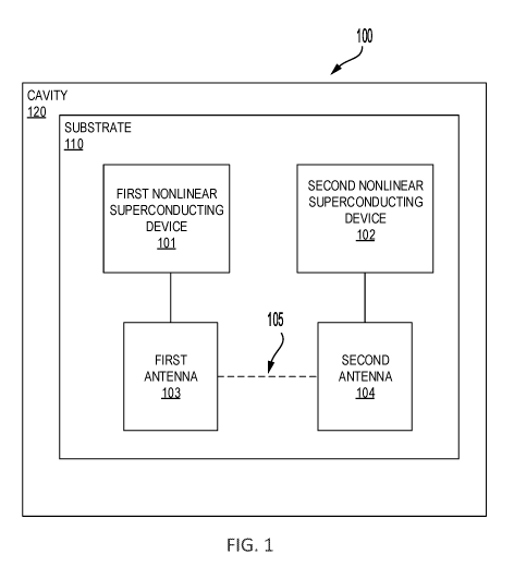
FIG. 1 is a block diagram of a nonlinear superconducting circuit 100,
according to some
embodiments. The nonlinear superconducting circuit 100 includes at least a
first nonlinear
superconducting device 101, a second nonlinear superconducting device 102, a
first antenna 103,
a second antenna 104, a substrate 110, and a cavity 120. It should be
appreciated that
embodiments need not include all of the components shown in FIG. 1. For
example, some
embodiments may not include the cavity 120 and/or the antennas 103/104.
The first nonlinear superconducting device 101 is a nonlinear device that
exhibits a
positive anharmonicity. In some embodiments, a positive anharmonicity refers
to the fourth order
term of the potential having a positive, non-zero value. In some embodiments,
the nonlinear
device that exhibits a positive anharmonicity uses an external magnetic field
to create the
positive anharmonicity. For example, an external magnetic field may be
threaded through a loop
or ring of the nonlinear device. Some examples of nonlinear superconducting
devices that are
capable of exhibiting positive anharmonicity include superconducting nonlinear
asymmetric
inductive elements (SNAILs), fluxonium qubits, radio frequency (RF)
superconducting quantum
interference devices (SQUIDS), and capacitively-shunted flux qubits.
The second nonlinear superconducting device 102 is a nonlinear device that
exhibits a
negative anharmonicity. In some embodiments, a negate anharmonicity refers to
the fourth order
term of the potential having a negative, non-zero value. Some examples of
nonlinear
superconducting devices that are capable of exhibiting negative anharmonicity
include SNAILs,
transmons, and SQUID transmons.
In some embodiments, the first and second nonlinear superconducting devices
101/102
are manufactured to have the respective anharmonicity properties.
Alternatively, the
anharmonicity properties of the nonlinear superconducting devices may be
controlled at the time
of operation. This may be achieved, for example, by using nonlinear
superconducting devices
that include at least one loop and threading an external magnetic field
through the at least one
loop. In some embodiments, an electromagnetic solenoid may be positioned near
the nonlinear
superconducting devices such that the external magnetic field created by the
solenoid is oriented
in a direction that is substantially perpendicular to the plane of the at
least one loop.
8
CA 03125986 2021-07-06
WO 2020/150348 PCT/US2020/013675
In some embodiments, the first and second nonlinear superconducting devices
101/102
comprise a superconducting material, such as aluminum formed on a substrate
110. The substrate
110 may, for example, be made from sapphire. In some embodiments, the first
and second
nonlinear superconducting devices 101/102 may be formed on the same substrate
110, as
illustrated in FIG. 1. In other embodiments, the first nonlinear
superconducting device 101 and
the second nonlinear superconducting device 102 may be formed on two different
substrates.
In some embodiments, the nonlinear superconducting circuit 100 includes the
cavity 120.
The cavity 120 may be, for example a three-dimensional (3D) resonator that
supports one or
more microwave frequencies. The substrate 110 on which the first and second
superconducting
devices 101/102 are formed may be suspended in the three-dimensional
resonator. However,
embodiments are not limited to 3D cavity resonators. Some embodiments use two-
dimensional,
planar superconducting resonators and circuits.
In some embodiments, the nonlinear superconducting circuit 100 includes a
first antenna
103 and a second antenna 104. The first antenna 103 is coupled to the first
nonlinear
superconducting device 101. The first antenna 103 enables microwave signals
supported by the
cavity 120 to couple to the first nonlinear superconducting device 101. The
second antenna 104
is coupled to the second nonlinear superconducting device 102. The second
antenna 104 enables
microwave signals supported by the cavity 120 to couple to the second
nonlinear
superconducting device 102. In some embodiments, the first antenna 103 and the
second antenna
104 are formed on the same substrate 110 as the first and second nonlinear
superconducting
device 101/102, as illustrated in FIG. 1. In other embodiments, the first
antenna 103 and the first
nonlinear superconducting device 101 are formed on a first substrate and the
second antenna 104
and the second nonlinear superconducting device 101 are formed on a second
substrate that is
different from the first substrate.
In some embodiments, the first and second antenna 103/104 may each include
multiple
portions. For example, a first portion of the first antenna 103 may be located
on a first side of the
first nonlinear superconducting device 101 and the second portion of the first
antenna 103 may
be located on a second side, opposite the first side, of the first nonlinear
superconducting device
101. In this way, the first portion and the second portion of the first
antenna 103 may be
connected to opposite sides of the first nonlinear superconducting device.
Similarly, a first
9
CA 03125986 2021-07-06
WO 2020/150348 PCT/US2020/013675
portion and a second portion of the second antenna may be connected to
opposite sides of the
second nonlinear superconducting device.
In some embodiments, the first and second antennas 103/104 may include a
superconducting pad formed from the same superconducting material (e.g.,
aluminum) as is used
to form the first and second nonlinear superconducting devices 101/102.
In some embodiments, a portion of the first antenna 103 is physically
connected to a
portion of the second antenna 104 by a superconducting connecting member 105.
In some
embodiments, the superconducting connecting member 105 may be a wire of
superconducting
material formed on the substrate 110.
FIG. 2A is a schematic diagram of a nonlinear superconducting circuit 200,
according to
some embodiments. The nonlinear superconducting circuit 200 includes a
transmon 201 as the
nonlinear superconducting device with a negative anharmonicity and a SNAIL 202
as the
nonlinear superconducting device with a positive anharmonicity. A first
antenna coupled to the
transmon 201 is formed by a first antenna portion 203 and a second antenna
portion 205. A
second antenna coupled to the SNAIL 202 is formed by the second antenna
portion 205 and a
third antenna portion 204. The second antenna portion 205 is shared between
the first antenna
and the second antenna. FIG. 2B is an equivalent circuit diagram 250 of the
nonlinear
superconducting circuit 200.
FIG. 3A is a schematic diagram of a SNAIL 300 that may be used in the
nonlinear
superconducting circuits 100 or 200, according to some embodiments. The SNAIL
300 includes
a superconducting ring 301 with two nodes 311 and 312. There are two path
along two different
portions of the superconducting ring 301 that connect the first node 331 and
the second node
312.
The first ring portion includes multiple Josephson junctions 305-307 connected
in series.
In some embodiments, there are no other circuit elements between one Josephson
junction and
the next Josephson junction. For example, a Josephson junction is a dipole
circuit element (i.e., it
has two nodes). A first node of a first Josephson junction 305 is directly
connected to the first
node 311 of the SNAIL, which may lead to some other external circuit element
(such as a portion
of the antenna). A second node of the first Josephson junction 305 is directly
connected to a first
node of a second Josephson junction 306. A second node of the second Josephson
junction 306 is
directly connected to a first node of a third Josephson junction 307. A second
node of the third
CA 03125986 2021-07-06
WO 2020/150348 PCT/US2020/013675
Josephson junction 307 is directly connected to a second node 312 of the
SNAIL, which may
lead to some other external circuit element (such as a portion of the
antenna).
While FIG. 3A illustrates the first ring portion including three Josephson
junctions, any
suitable number of Josephson junctions greater than one may be used. For
example, three, four,
five, six, or seven Josephson junctions may be used. Three Josephson junctions
are selected for
the example shown because three Josephson junctions is the lowest number of
Josephson
junctions (other than zero or one) that can be formed using a Dolan bridge
process of
manufacturing, which is used in some embodiments.
In some embodiments, Josephson junctions 305-307 are formed to be identical.
For
example, the tunneling energies, the critical current, and the size of the
Josephson junctions 305-
307 are all the same.
The second ring portion of the SNAIL 300 includes a single Josephson junction
308. In
some embodiments, there are no other circuit elements in the second ring
portion. A first node of
a single Josephson junction 308 is directly connected to the first node 311 of
the SNAIL, which
may lead to some other external circuit element (such as a portion of the
antenna). A second
node of the single Josephson junction 308 is directly connected to the second
node 312 of the
SNAIL, which may lead to some other external circuit element (such as a
portion of the antenna).
The single Josephson junction 308 has a smaller tunneling energy than each of
Josephson
junctions 305-307. For this reason, the single Josephson junction 308 may be
referred to as a
"small" Josephson junction and Josephson junctions 305-307 may be referred to
as "large"
Josephson junctions. The terms "large" and "small" are relative terms that are
merely used to
label the relative size of Josephson junction 308 as compared to Josephson
junctions 305-307.
The Josephson energy and the Josephson junction size are larger in the large
Josephson junction
than in the small Josephson junction. The parameter a is introduced to
represent the ratio of the
small Josephson energy to the large Josephson energy. Thus, the Josephson
energy of the large
Josephson junctions 305-307 is Ej and the Josephson energy of the small
Josephson junction 108
is aEj, where 0 < a <1.
FIG. 3B illustrates the circuit element symbol for the SNAIL 300. The
parameters that
characterize the SNAIL 300 are the Josephson energy Ej and the superconducting
phase
difference, cp, of the small Josephson junction 308. Of note is the fact that
the SNAIL 300 has
only two nodes 311 and 312.
11
CA 03125986 2021-07-06
WO 2020/150348 PCT/US2020/013675
FIG. 3C is a scanning electron microscope image of an example SNAIL 300. The
image
in FIG. 3C is a mirror image of the SNAIL 300 shown in FIG. 3A. In other
words, the single
small Josephson junction is on the left side in FIG. 3A, not the right side as
it is in FIG. 3A. The
single small Josephson junction is formed using a single Dolan bridge 320. The
three large
Josephson junctions 305-307 are formed from a first Dolan bridge 321 and a
second Dolan
bridge 322. The Dolan bridge fabrication technique has the advantage of being
able to reliably
fabricate junctions with particular parameters while only requiring a single
double-angle
evaporation act. If N Dolan bridges are formed in series, 2N ¨ 1 Josephson
junctions are formed.
This is because junctions are formed underneath each bridge and between
adjacent bridges.
Thus, the simplest way to form a plurality of Josephson junctions using Dolan
bridges is to form
two Dolan bridges.
The SNAIL 300 may controlled at least in part by threading a DC magnetic flux
(1)õt
through the superconducting ring 301. In some embodiments, a magnetic flux
generation device
(not shown) may be positioned in proximity to the superconducting ring. For
example, an
electrical coil (e.g., a solenoid) may be formed in proximity to the ring 101.
The coil may be next
to the ring 101 and in the same plane as ring 101. Alternatively, a coil may
be under the ring 101
in a different layer of the device 100, e.g., above or below the plane of the
superconducting ring
301.
As mentioned above, any number of large Josephson junctions may be used in the
SNAIL 300. For a SNAIL with n large Josephson junctions, the SNAIL has an
inductive energy
given by:
USNAIL((P) = ¨aEj cos(p) ¨ nEj cos ((Pext¨(P¨n) , (Eqn. 1)
where cp is the superconducting phase across the single small Josephson
junction 108, (Pext =
27r cl'ext ictio is the reduced applied magnetic flux, and (Po = h/2e is the
magnetic flux quantum.
Eqn. 1 indicates that the potential is a function of a single degree of
freedom (cp). This is because
dynamics due to any intra-array modes are eliminated and only common
excitations across the
array of n Josephson junctions are considered. This reduction is valid when E1
>> Ec for each
junction, where Ec = e2 /2C1 is the Coulomb charging energy of the junction
with capacitance
Cj, and when Co << Cj/n2, where Cois the capacitance to ground of each island
between
junctions. Some embodiments meet all of these requirements.
12
CA 03125986 2021-07-06
WO 2020/150348 PCT/US2020/013675
In some embodiments, the parameters a and (Do may be selected such that the
SNAIL
300 has properties desirable for its application. For example, for a-0.8 and
(1)õt-0.5(1)0, the
SNAIL 300 will have a double-well potential, which is undesirable due to the
resulting hysteresis
affects. But the parameters can be adjusts to create a potential with a single
minimum. Moreover,
the potential may simultaneously be tuned to have a positive anharmonicity in
the fourth-order
term (e.g., for a-0.2 and (1)õt-0.4(1)0).
To select desirable parameters, the potential of Eqn. 1 is Taylor expanded
about its
minimum value Omin to obtain the effective potential for Cp = ¨
ue f f (0)
= c2Cp2 + c3Cp3 + c4Cp4 + = , Eqn. (2)
Ej
where (c2, c3, c4,...) are numerically determinable coefficients whose
specific values
depend on n (which is three in the illustrated embodiments), a, and (1)õt.
It is noted that for n = 1 (e.g., a SQUID) c3 = 0 because the potential is a
pure cosine
irrespective of the values of a, and (1)õt. Additionally, in the limit n >> 1,
the array of multiple
large Josephson junctions act as a linear inductance and the potential
approaches that of a
fluxonium qubit/RF SQUID regime. While embodiments may include any number of
large
Josephson junctions so long as n > 1 and the number is not in the regime where
n >> 1, the
example described herein is focused on the case where n = 3. Embodiments are
not however,
limited to this example embodiment.
FIG. 4A is a greyscale color map for the fourth-order phase term, c4, of the
potential as a
function of the parameter a and the external DC magnetic flux, (1)ext for n =
3. FIG. 4B is a
greyscale color map for the difference between the second-order (quadratic)
phase term, c2, of
the potential and the effective fourth-order (quartic) phase term, c,' as a
function of the
e f f
parameter a and the external DC magnetic flux, (I) ext for n = 3, where c4 =
c4 ¨ ¨ (the c3
3c2
term is small, making the effective fourth-order phase term not too dissimilar
from the actual
fourth-order phase term). Thus, in some embodiments, a quartic coefficient of
the potential of the
SNAIL 300 is equal to a quadratic coefficient of the potential of the SNAIL
300. In some
embodiments, the quartic coefficient is the aforementioned effective quartic
coefficient, which is
a function of the quadratic coefficient, the cubic coefficient and the actual
quartic coefficient of
the potential of the SNAIL 300.
13
CA 03125986 2021-07-06
WO 2020/150348 PCT/US2020/013675
These two maps of FIG. 4A-4B can be numerically searched to simultaneously
obtain
two desired criteria. This first criterion is for c4 to be positive and non-
zero, corresponding to the
dark grey area encircled by line 410 in FIG. 4A. The second criterion is to
have c4eff. = c2,
which corresponds to the light area between lines 420 and 422 in FIG. 4B. In
some
embodiments, a may be restricted to 0 <a <0.50, 0.1 < a <0.50, 0.15 <a <0.40,
0.18 <
a < 0.34, or 0.185 <a <0.33. In some embodiments, a may be selected to be
substantially
equal to 0.18, 0.185, 0.2, or 0.33. In some embodiments, the external magnetic
field, (1)ext, may
be restricted to 0.4 < (1)ext < 0.50, 0.45 < (1)ext < 0.50, 0.47 < (1)ext <
0.50, or 0.48 <
(1)ext <0.50.
The above values may be of interest for a SNAIL with three Josephson
junctions. In
particular, the value of alpha may be 0.18 < a <0.33. However, other
embodiments may use a
SNAIL with a larger number of Josephson junctions. In an embodiment with N
Josephson
junctions, the range of interest may be between, and including, the values 1/N
and 1/2(1/N +
1/N3). However, embodiments are not limited to this particular range.
In addition to the above criteria, some embodiments have the SNAIL resonance
frequency equal to the transmon resonance frequency. This requirement is
equivalent to the
inductance of the transmon (Ljt) being equal to the inductance of the SNAIL
(Lis) (see FIG. 2B).
In some embodiments, the SNAIL 300 resonance frequency may be tuned using the
external
magnetic flux through the superconducting ring 301 of the SNAIL 300.
When the above conditions are met, the nonlinear superconducting circuit 200
exhibits a
symmetric mode and an asymmetric mode. FIG. 5A illustrates the symmetric mode
of the
nonlinear superconducting circuit 200, where the current through the transmon
and the SNAIL
occur in phase with the cavity excitation. FIG. 5B illustrates the asymmetric
mode of the
nonlinear superconducting circuit 200, wherein the current through the
transmon is in phase with
the cavity excitation and the current through the SNAIL is 180-degrees out-of-
phase with the
cavity excitation. Thus, the symmetric mode of FIG. 5A couples linearly with
the cavity mode
and the asymmetric mode of FIG. 5B does not couple linearly with the cavity
mode. In some
embodiments, this coupling can be switched such that the asymmetric mode of
FIG. 5B couples
linearly with the cavity mode and the symmetric mode of FIG. 5A does not
couple linearly with
the cavity mode.
14
CA 03125986 2021-07-06
WO 2020/150348 PCT/US2020/013675
The Hamiltonian of the superconducting circuit 200 written in terms of the
symmetric
and asymmetric eigenmodes is as follows:
11121 = g4t[cPs(S + St) + (PA(A + At) + (Pc(C + Ct)]4
+ g4s[Os(S + St) ¨ (PA(A + At) + Oc(C + Ct)]4
where S and St are the annihilation and creation operators, respectively, for
the symmetric
eigenmode of the circuit 200; A and At are the annihilation and creation
operators, respectively,
for the asymmetric eigenmode of the circuit 200; and C and Ct are the
annihilation and creation
operators, respectively, for the cavity mode of the circuit 200. In the above
Hamiltonian, 94t =
¨Eft/4! h and g4s = c4Ejs/4! h. Thus, 94t and g4s have opposite signs. When
the Hamiltonian
is expanded, the self-Kerr and cross-Kerr terms are equal to zero when the
condition g4s =
¨94t = g4 > 0. In some embodiments, g4s may be tuned using the external
magnetic flux
and/or the ratio a of the SNAIL. In some embodiments, 94t may be set at the
time of
manufacturing by setting the capacitance and/or size of the superconducting
pads forming the
antennas of the transmon and/or the critical current, lc, of the transmon.
When the first condition (Ls = Lt) and the second condition (94s = ¨94t = g4 >
0) are
met, and the Hamiltonian is expanded, the terms with an odd number of OA will
not cancel (due
to the difference in signs in the asymmetric terms of the Hamiltonian), but
all terms with an even
number of OA do cancel. Thus, constructive interference results in only the
following four-wave-
mixing terms being non-zero:
cop = ao, ¨ (DA Heft, = 24g4004A(C2At + Ct2A)
cop = (DA Heft, = 2494004A(2CtC)(At + A)
Thus, by forming a nonlinear superconducting circuit with two nonlinear
superconducting devices that satisfy the above two conditions, a pure four-
wave-mixing
interaction may be engineered without the negative influences of dephasing and
frequency shifts
caused be the self-Kerr and cross-Kerr interactions, which are canceled out
due to the symmetry
of the circuit.
The above discussion focuses on the example embodiment of FIG. 2 where a
transmon
and a SNAIL are used as the two nonlinear superconducting devices. However,
embodiments are
not so limited. As discussed above, there are a number of devices that may be
used to exhibit
positive anharmonicity and negative anharmonicity. In some embodiments, it may
be desirable
CA 03125986 2021-07-06
WO 2020/150348 PCT/US2020/013675
for both the first nonlinear superconducting device and the second nonlinear
superconducting
device to include a superconducting loop. By both devices including a
superconducting ring such
that both devices may be actively tuned using an external magnetic flux. In
some embodiments
the first nonlinear superconducting device and the second nonlinear
superconducting device may
include superconducting rings of different sizes/areas such that the effects
of the external
magnetic flux is different between the two devices, allowing for better tuning
of the above
parameters using a single magnetic flux source (e.g., a solenoid).
FIG. 6A illustrates a nonlinear superconducting circuit 600, according to some
embodiments. The superconducting circuit 600 includes a SNAIL 601, a SQUID
602, a first
antenna portion 603, a second antenna portion 605, a third antenna portion
604, a fourth antenna
portion 606, a superconducting connecting member 607, a substrate 610, a
cavity 620, a
magnetic flux source 615, a microwave pin 612, and a transmission line 611.
The superconducting circuit 600 includes the SNAIL 601 and the SQUID 602 as
the first
and second nonlinear superconducting devices, respectively. Thus, both
nonlinear
superconducting devices of the nonlinear superconducting circuit 600 include a
superconducting
ring through which an external magnetic flux is thread. The superconducting
circuit 600 includes
a magnetic flux source 615 for generating the external magnetic flux that can
be used to control
one or more parameters of the SNAIL 601 and the SQUID 602. In some
embodiments, the
magnetic flux source 615 is a solenoid that is located outside of the cavity
620. The magnetic
flux source 615 is located above the substrate 610 and oriented such that the
axis of the solenoid
is perpendicular to the upper surface of the substrate 610.
The SNAIL 601 is physically connected to a first antenna that includes the
first antenna
portion 603 and the second antenna portion 605. The first antenna couples the
SNAIL 601 to the
microwave signals supported by the cavity 620. The first antenna portion 603
and the second
antenna portion 605 are attached on opposite sides of the SNAIL 601.
The SQUID 602 is physically connected to a second antenna that includes the
third
antenna portion 604 and the fourth antenna portion 606. The second antenna
couples the SQUID
602 to the microwave signals supported by the cavity 620. The third antenna
portion 604 and the
fourth antenna portion 606 are attached on opposite sides of the SQUID 602.
Additionally, the
second antenna portion 605 and the fourth antenna portion 606 are physically
connected by a
superconducting connecting member 607.
16
CA 03125986 2021-07-06
WO 2020/150348 PCT/US2020/013675
Microwave signals that drive the nonlinear superconducting circuit 600 are
coupled to the
cavity 620 via the transmission line 611 via the microwave pin 612, which
interfaces with an
aperture of the cavity 620. The substrate 610 is suspended in the cavity 620
such that the two
antennas are near the center of the cavity 620.
FIG 6B is an optical microscope image of the portion of the substrate that
includes the
SNAIL 601, the SQUID 602, and the two antennas.
FIG. 7 is a spectrogram resulting from performing a heterodyne measurement of
the
cavity microwave signals as function of the scanning frequency of a vector
network analyzer
(VNA) and the current through the solenoid controlling the external magnetic
field flux. Phase
jumps (e.g., like those at points 710 and 712) in the spectrogram correspond
with resonances
where a mode of the nonlinear superconducting circuit 600 actively couples to
the transmission
line 611.
FIG. 8 is a two-tone spectrogram resulting from fixing the VNA frequency at
approximately 7.6 GHz and applying a second microwave frequency using a
microwave
generator while sweeping the current applied to the solenoid controlling the
external magnetic
field flux. Phase jumps from positive phases (e.g., point 810) to negative
phases (e.g., point 812)
correspond to an operating points for performing four-wave-mixing according to
some
embodiments. Note that there are multiple operating points corresponding to
different solenoid
currents, any of which may be used as an operating point for four-wave-mixing.
FIG. 9A and FIG. 9B are zoomed in portions of the two-tone spectrogram
corresponding
to the region of Box A of FIG. 8 for the symmetric mode and asymmetric mode,
respectively, of
the nonlinear superconducting circuit 600. This region corresponds to two
different operating
points 910 and 912 with the same associated microwave frequency, but different
external
magnetic flux values (and therefore different solenoid current values).
While the above discussion has focused on the four-wave mixing terms that
correspond
to the annihilation of two cavity microwave photons to form an anti-symmetric
quanta in the
superconducting circuit (e.g., the C2At term) there are other terms that may
be used under the
same cancellation conditions if pumped at higher frequencies. These additional
terms correspond
to higher order terms of the Hamiltonian. FIG. 10 illustrates a spectrogram
showing these higher
order operating points. For example, terms corresponding to St A t2 C, Atst,
SC, and ASCt
17
CA 03125986 2021-07-06
WO 2020/150348 PCT/US2020/013675
interactions are shown in FIG. 10. To utilize these interactions, the
nonlinear superconducting
circuit is operated at the corresponding frequency and external magnetic flux.
Having thus described several aspects and embodiments of the technology set
forth in the
disclosure, it is to be appreciated that various alterations, modifications,
and improvements will
readily occur to those skilled in the art. Such alterations, modifications,
and improvements are
intended to be within the spirit and scope of the technology described herein.
For example, those
of ordinary skill in the art will readily envision a variety of other means
and/or structures for
performing the function and/or obtaining the results and/or one or more of the
advantages
described herein, and each of such variations and/or modifications is deemed
to be within the
scope of the embodiments described herein. Those skilled in the art will
recognize, or be able to
ascertain using no more than routine experimentation, many equivalents to the
specific
embodiments described herein. It is, therefore, to be understood that the
foregoing embodiments
are presented by way of example only and that, within the scope of the
appended claims and
equivalents thereto, inventive embodiments may be practiced otherwise than as
specifically
described. In addition, any combination of two or more features, systems,
articles, materials,
kits, and/or methods described herein, if such features, systems, articles,
materials, kits, and/or
methods are not mutually inconsistent, is included within the scope of the
present disclosure.
Also, as described, some aspects may be embodied as one or more methods. The
acts
performed as part of the method may be ordered in any suitable way.
Accordingly, embodiments
may be constructed in which acts are performed in an order different than
illustrated, which may
include performing some acts simultaneously, even though shown as sequential
acts in
illustrative embodiments.
All definitions, as defined and used herein, should be understood to control
over
dictionary definitions, definitions in documents incorporated by reference,
and/or ordinary
meanings of the defined terms.
The indefinite articles "a" and "an," as used herein in the specification and
in the claims,
unless clearly indicated to the contrary, should be understood to mean "at
least one."
The phrase "and/or," as used herein in the specification and in the claims,
should be
understood to mean "either or both" of the elements so conjoined, i.e.,
elements that are
conjunctively present in some cases and disjunctively present in other cases.
Multiple elements
listed with "and/or" should be construed in the same fashion, i.e., "one or
more" of the elements
18
CA 03125986 2021-07-06
WO 2020/150348 PCT/US2020/013675
so conjoined. Other elements may optionally be present other than the elements
specifically
identified by the "and/or" clause, whether related or unrelated to those
elements specifically
identified. Thus, as a non-limiting example, a reference to "A and/or B", when
used in
conjunction with open-ended language such as "comprising" can refer, in one
embodiment, to A
only (optionally including elements other than B); in another embodiment, to B
only (optionally
including elements other than A); in yet another embodiment, to both A and B
(optionally
including other elements); etc.
As used herein in the specification and in the claims, the phrase "at least
one," in
reference to a list of one or more elements, should be understood to mean at
least one element
selected from any one or more of the elements in the list of elements, but not
necessarily
including at least one of each and every element specifically listed within
the list of elements and
not excluding any combinations of elements in the list of elements. This
definition also allows
that elements may optionally be present other than the elements specifically
identified within the
list of elements to which the phrase "at least one" refers, whether related or
unrelated to those
elements specifically identified. Thus, as a non-limiting example, "at least
one of A and B" (or,
equivalently, "at least one of A or B," or, equivalently "at least one of A
and/or B") can refer, in
one embodiment, to at least one, optionally including more than one, A, with
no B present (and
optionally including elements other than B); in another embodiment, to at
least one, optionally
including more than one, B, with no A present (and optionally including
elements other than A);
in yet another embodiment, to at least one, optionally including more than
one, A, and at least
one, optionally including more than one, B (and optionally including other
elements); etc.
Also, the phraseology and terminology used herein is for the purpose of
description and
should not be regarded as limiting. The use of "including," "comprising," or
"having,"
"containing," "involving," and variations thereof herein, is meant to
encompass the items listed
thereafter and equivalents thereof as well as additional items.
19