Note: Descriptions are shown in the official language in which they were submitted.
1
DIE FORA PRINTHEAD
FIELD
[0001] The subject disclosure relates to a die for a printhead.
BACKGROUND
[0001a] A printing system, as one example of a fluid ejection system, may
include
a printhead, an ink supply which supplies liquid ink to the printhead, and an
electronic controller which controls the printhead. The printhead ejects drops
of print
fluid through a plurality of fluidic actuators or orifices onto a print
medium. The
printheads may include thermal or piezo printheads that are fabricated on
integrated
circuit wafers or dies. Drive electronics and control features are first
fabricated, then
the columns of heater resistors are added and finally the structural layers,
for
example, formed from photo-imageable epoxy, are added, and processed to form
microfluidic ejectors, or drop generators. In some examples, the microfluidic
ejectors
are arranged in at least one column or array such that properly sequenced
ejection
of ink from the orifices causes characters or other images to be printed upon
the
print medium as the printhead and the print medium are moved relative to each
other. Other fluid ejection systems include three-dimensional print systems or
other
high precision fluid dispensing systems for example for life science,
laboratory,
forensic or pharmaceutical applications. Suitable fluids may include inks,
print agents
or any other fluid used by these fluid ejection systems.
SUMMARY
[0001b] Accordingly, in one aspect there is provided a die for a printhead,
comprising: a plurality of fluidic actuator arrays, proximate to a plurality
of fluid feed
holes; a plurality of address lines, proximate to a plurality of logic
circuits on a low-
voltage side of the plurality of fluid feed holes; and an address decoder
circuit that
couples to at least a portion of the address lines to select a fluidic
actuator in a fluidic
actuator array for firing, wherein: the address decoder circuit is customized
to select
a different address for each fluidic actuator in the fluidic actuator array;
and a logic
circuit that triggers a driver circuit located in a high-voltage side of the
plurality of
fluid feed holes opposite the low-voltage side, based, at least in part, on a
bit value
Date Recue/Date Received 2023-01-22
1 a
for the fluidic actuator array, the fluidic actuator selected by the address
decoder
circuit, and a firing signal.
[0001c] According to another aspect there is provided a method for forming a
die
for a printhead, comprising: etching a plurality of fluid feed holes in a line
down a
substrate; and depositing a plurality of layers on the substrate to form: a
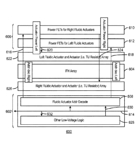
plurality of
fluidic actuator arrays, proximate to the plurality of fluid feed holes; a
plurality of
address lines, proximate to a plurality of logic circuits in a low-voltage
region
disposed on one side of the plurality of fluid feed holes; an address decoder
circuit
that couples to at least a portion of the plurality of address lines to select
a fluidic
actuator in a fluidic actuator array for firing, wherein the address decoder
circuit is
customized to select a different address for each fluidic actuator in the
fluidic
actuator array; and a logic circuit in the plurality of logic circuits that
triggers a driver
circuit located in a high-voltage region on an opposite side of the plurality
of fluid
feed holes based, at least in part, on a bit value for the fluidic actuator
array, the
fluidic actuator selected by the address decoder circuit, and a firing signal.
[0001d] According to another aspect there is provided a printhead comprising a
die, comprising: a plurality of fluidic actuator arrays, proximate to a
plurality of fluid
feed holes; a plurality of address lines, proximate to a plurality of logic
circuits in a
low-voltage region disposed on one side of the plurality of fluid feed holes;
a plurality
of address bits, wherein each address bit sets a value of one of the plurality
of
address lines; an address decoder circuit that couples to at least a portion
of the
address lines to select a fluidic actuator in a fluidic actuator array for
firing, wherein
the address decoder circuit is customized to select a different address for
each
fluidic actuator in the fluidic actuator array; and a logic circuit in the
plurality of logic
circuits that triggers a driver circuit located in a high-voltage region on an
opposite
side of the plurality of fluid feed holes based, at least in part, on a bit
value for the
fluidic actuator array, the fluidic actuator selected by the address decoder
circuit, and
a firing signal.
Date Recue/Date Received 2023-01-22
lb
BRIEF DESCRIPTION OF THE DRAWINGS
[0002] Certain examples are described in the following detailed description
and in
reference to the drawings, in which:
[0003] Fig. IA is a view of a part of a die used for a prior art inkjet
printhead;
[0004] Fig. 1B is an enlarged view of a portion of the die;
[0006] Fig. 2A is a view of an example of a die used for a printhead;
[0006] Fig. 2B is an enlarged view of a portion of the die;
[0007] Fig. 3A is a drawing of an example of a printhead including a black
die that
is mounted in a potting compound;
[0008] Fig. 3B is a drawing of an example of a printhead including three
dies,
which may be used for three colors of ink;
[0009] Fig. 3C shows cross-sectional views of the printheads including the
mounted dies through solid sections and through sections having fluid feed
holes;
Date Recue/Date Received 2023-01-22
CA 03126051 2021-07-07
WO 2020/162909
PCT/US2019/016777
2
[0010] Fig. 4 is an example of a printer cartridge that incorporates the
printhead
described with respect to Fig. 3B;
[0011] Fig. 5 is a schematic diagram of an example of a set of four
primitives,
termed a quad primitive;
[0012] Fig. 6 is a drawing of an example of a layout of the die circuitry,
showing
the simplification that can be achieved by a single set of fluidic actuator
circuitry;
[0013] Fig. 7 is a drawing of an example of a circuit floorplan
illustrating a number
of die zones for a color die;
[0014] Fig. 8 is a schematic diagram of an example of address decoding on a
die;
[0015] Fig. 9 is a schematic diagram of an example of another
implementation of
address decoding on a die;
[0016] Fig. 10 is a schematic diagram of an example of another
implementation of
address decoding on a die;
[0017] Fig. 11 is a drawing of an example of a black die showing the
formation of
vias from the address lines to the logic circuitry;
[0018] Fig. 12 is a drawing of an example of a black die showing an offset
in
address order of primitives between fluidic actuator columns on each side of
the fluid
feed hole array, in accordance with example;
[0019] Fig. 13 is an example of a circuit diagram of a die;
[0020] Fig. 14 is a drawing of an example of a die showing the interface
pads and
logic locations used to load data and control signals into the die;
[0021] Fig. 15 is a schematic diagram an example of the serial loading of
data
into the data store;
[0022] Fig. 16 is a circuit diagram an example of a logical function for
firing a
single fluidic actuator in a primitive;
[0023] Fig. 17 is an example of a schematic diagram of memory bits
shadowing
primitive blocks in the data store;
[0024] Fig. 18 is an example of a block diagram of the configuration
register, the
memory configuration register, and the status register;
[0025] Fig. 19 is a schematic drawing of an example of a die showing a
sense
bus for reading and programming memory bits and accessing thermal sensors;
CA 03126051 2021-07-07
WO 2020/162909
PCT/US2019/016777
3
[0026] Fig. 20 is a circuit diagram of an example of a high-voltage
protection
switch used to protect lower voltage MOS circuitry from damage from high-
voltage;
[0027] Fig. 21 is a circuit diagram of an example of a memory voltage
regulator;
[0028] Fig. 22A is a process flow diagram of an example of a method for
forming
a printhead component;
[0029] Fig. 22B is a process flow diagram of the components formed by the
layers of block 2204 in the method;
[0030] Fig. 22C is a process flow diagram of the combined method showing
the
layers and structures that are formed;
[0031] Fig. 23 is a process flow diagram of an example of a method for
loading
data into a printhead component; and
[0032] Fig. 24 is a process flow diagram of an example of a method for
writing a
memory bit in a printhead component.
DETAILED DESCRIPTION OF SPECIFIC EXAMPLES
[0033] Printheads are formed using fluidic actuators, such as microfluidic
ejectors
and microfluidic pumps. The fluidic actuators can be based on thermal
resistors or
piezoelectric technologies, which may force the ejection of a droplet from a
nozzle or
force a small amount of fluid to move out of a pumping chamber. The fluidic
actuators are formed using long, narrow pieces of silicon, termed dies or
print
components herein. In examples described herein, a microfluidic ejector is
used as
an ejector for a nozzle in a die, used for printing and other applications.
For example,
printheads can be used as fluid ejection devices in two-dimensional and three-
dimensional printing applications and other high precision fluid dispensing
systems
including pharmaceutical, laboratory, medical, life science and forensic
applications.
While this disclosure may refer to inkjet and ink applications, the principles
disclosed
herein are to be associated with any fluid propelling or fluid ejecting
application, not
limited to ink.
[0034] The cost of printheads is often determined by the amount of silicon
used in
the dies, as the cost of the die and the fabrication process increase with the
total
amount of silicon used in a die. Accordingly, lower cost printheads may be
formed by
moving functionality off the die to other integrated circuits, allowing for
smaller dies.
CA 03126051 2021-07-07
WO 2020/162909
PCT/US2019/016777
4
[0035] Many current dies have an ink feed slot in the middle of the die to
bring ink
to the fluidic actuators. The ink feed slot generally provides a barrier to
carrying
signals from one side of an die to another side of a die, which often requires
duplicating circuitry on each side of the die, further increasing the size of
the die. In
this arrangement, fluidic actuators on one side of the slot, which may be
termed left
or west, have independent addressing and power bus circuits from fluidic
actuators
on the opposite side of the ink feed slot, which may be termed right or east.
[0036] Examples described herein provide a new approach to providing fluid
to
the fluidic actuators of the drop ejectors. In this approach, the ink feed
slot is
replaced with an array of fluid feed holes disposed along the die, proximate
to the
fluidic actuators. The array of fluid feed holes disposed along the die may be
termed
a feed zone, herein. As a result, signals can be routed through the feed zone,
between the fluid feed holes, for example, from the logic circuitry located on
one side
of the fluid feed holes to printing power circuits, such as field-effect
transistors
(FETs), located on the opposite side of the fluid feed holes. This is termed
cross-slot
routing herein. The circuitry to route the signals includes traces provided in
layers
between adjacent ink or fluid feed holes.
[0037] As used herein, a first side of the die and a second side of the die
denote
the long edges of the die that are in alignment with the fluid feed holes,
which are
placed near or at the center of the die. Further, as used herein, the fluidic
actuators
are located on a front face of the die, and the ink or fluid is fed to the
fluid feed holes
from a slot on the back face of the die. Accordingly, the width of the die is
measured
from the edge of the first side of the die to the edge of the second side of
the die.
Similarly, the thickness of the die is measured from the front face of the die
to the
back face of the die.
[0038] The cross-slot routing allows for the elimination of duplicate
circuitry on the
die, which can decrease the width of the die, for example, by 150 micrometers
(pm)
or more. In some examples, this may provide a die with a width of about 450 pm
or
about 360 pm, or less. In some examples, the elimination of duplicate
circuitry by the
cross-slot routing may be used to increase the size of the circuitry on the
die, for
example, to enhance performance in higher value applications. In these
examples,
the power FETs, the circuit traces, power traces, and the like, may be
increased in
CA 03126051 2021-07-07
WO 2020/162909
PCT/US2019/016777
size. This may provide dies that are capable of higher droplet weights.
Accordingly,
in some examples, the dies may be less than about 500 pm, or less than about
750 pm, or less than about 1000 pm in width.
[0039] The thickness of the die from the front face to the back face is
also
decreased by the efficiencies gained from the use of the fluid feed holes.
Previous
dies that use ink feed slots may be greater than about 675 pm, while dies
using the
fluid feed holes may be less than about 400 pm in thickness. The length of the
dies
may be about 10 millimeters (mm), about 20 mm, or about 20 mm, depending on
the
number of fluidic actuators used for the design. The length of the dies
includes space
at each end of the die for circuitry, accordingly the fluidic actuators occupy
a portion
of the length of the die. For example, for a black die of about 20 mm in
length, the
fluidic actuators may occupy about 13 mm, which is the swath length. A swath
length
is the width of the band of printing, or fluid ejection, formed as a printhead
is moved
across a print medium.
[0040] Further, the cross-slot routing allows the co-location of similar
devices for
increased efficiency and layout. The cross-slot routing optimizes power
delivery by
allowing left and right columns of fluidic actuators, to share power and
ground routing
circuits. However, a narrower die may be more fragile than a wider die.
Accordingly,
the die may be mounted in a polymeric potting compound that has a slot from a
reverse side to allow ink to flow to the fluid feed holes. In some examples,
the potting
compound is an epoxy, although it may be an acrylic, a polycarbonate, a
polyphenylene sulfide, and the like.
[0041] The cross-slot routing also allows for the optimization of circuit
layout. For
example, the high-voltage and low-voltage domains may be isolated on opposite
sides of the fluid feed holes allowing for improvements in reliability and
form factor
for the dies. The separation of the high-voltage and low-voltage domains may
decrease or eliminate parasitic voltages, crosstalk, and other issues that
affect the
reliability of the die. Further, a single instance of address data is conveyed
to logic
blocks which decode the address value uniquely for each side of an array of
fluid
feed holes.
[0042] To meet fluidic constraints and minimize effects of fluid flow to
multiple
fluidic actuators, such as fluidic cross-talk that can affect image quality,
the address
CA 03126051 2021-07-07
WO 2020/162909
PCT/US2019/016777
6
decode is offset for fluidic actuators on each respective side of the array of
fluid feed
holes. The address decoding may be customized for each group of fluidic
actuators,
or primitives, during fabrication of the die, for example, as a final step
during the
fabrication process. Other customizations may be used to determine which
fluidic
actuators are to fire from the values on the address lines.
[0043] The die used for a printhead, as described herein, uses resistors to
heat
fluids in a microfluidic ejector causing droplet ejection by thermal
expansion.
However, the dies are not limited to thermally driven fluidic actuators and
may use
piezoelectric fluidic actuators that are fed from fluid feed holes.
[0044] Further, the die may be used to form fluidic actuators for other
applications
besides a printhead, such as microfluidic pumps, used in analytical
instrumentation.
In this example, the fluidic actuators may be fed test solutions, or other
fluids, rather
than ink, from fluid feed holes. Accordingly, in various examples, the fluid
feed holes
and inks can be used to provide fluidic materials that may be ejected or
pumped by
droplet ejection from thermal expansion or piezoelectric activation.
[0045] In addition to the efficiencies gained by the cross routing of the
signals
from one side to the other, the dies described herein move logic circuits from
the die
to an external chip, or other support circuit. In various examples, the
external chip is
an application specific integrated circuit (ASIC) that is integrated into the
printer.
Further, individual colors are separated onto single dies versus incorporating
multiple
colors on a single die, which enables lower cost fluid manifolds for
delivering ink and
other fluids to the dies. Moving the thermal control loop off chip also
enables much
more complex thermal system behavior, while not increasing costs, such as the
ability to take and average multiple measurements, use relative setpoints,
enable
higher thermal resolution sensing, and increasing the number of sensors or
sense
zones on the individual dies and colors, among others. Associating the memory
bits
with decoding logic for addressing fluidic actuators enables the creation of
large
memory arrays at a low overhead cost.
[0046] In some examples, the memory bits are read using a sensor bus that
is
also used for external analog measurements, such as the thermal measurements,
to
further lower the cost. As the sensor bus is shared between various sensors,
such as
thermal sensors, crack detection sensors, and the memory bits, on-die, high-
voltage
CA 03126051 2021-07-07
WO 2020/162909
PCT/US2019/016777
7
protection circuitry prevents damage to low-voltage devices connected to the
sense
bus during a memory write. In some examples, an on-die voltage generator, or
memory voltage regulator, is used to write memory bits without the need for an
additional electrical interface from external circuitry.
[0047] Fig. lA is a view of a part of a die 100 used for a prior art inkjet
printhead.
The die 100 includes all circuitry to operate fluidic actuators 102 on both
sides of an
ink feed slot 104. Accordingly, all electrical connections are brought out on
pads 106
located at each end of the die 100. Fig. 1B is an enlarged view of a portion
of the die
100. As can be seen in this enlarged view, the ink feed slot 104 occupies a
substantial amount of space in the center of the die 100, increasing the width
108 of
the die 100.
[0048] Fig. 2A is a view of an example of a die 200 used for a printhead.
In
comparison with the die 100 of Fig. 1A, has an efficient and novel circuit lay-
out
wherein individual circuit blocks may have more functions, allowing the die
200 to be
relatively narrow and/or efficient, as described herein. In this design, some
functionality is provided to the die by an external circuit, such as an
application
specific integrated circuit (ASIC) 200.
[0049] In this example, the die 200 uses fluid feed holes 204 to provide
fluid, such
as inks, to the fluidic actuators 206 for ejection by thermal resistors 208.
As
described herein, the cross-slot routing allows circuitry to be routed along
silicon
bridges 210 between the fluid feed holes 204 and across the longitudinal axis
212 of
the die 200. In one example, this also allows the width 214 of the die 200 to
be
relatively small, for example, being less than about 420 pm, less than about
500 pm,
or less than about 750 pm, or less than about 1000 pm, for example between
about
330 pm and about 460 pm. The narrow width of the die 200 may decrease costs,
for
example, by lowering the amount of silicon used in the die 200.
[0050] As described herein, the die 200 also includes sensor circuitry for
operations and diagnostics. In some examples, the die 200 includes thermal
sensors
216, for example, placed along the longitudinal axis of the die near one end
of the
die, at the middle of the die, and near the opposite end of the die. In some
examples,
more thermal sensors 216 are used to improve thermal control.
CA 03126051 2021-07-07
WO 2020/162909
PCT/US2019/016777
8
[0051] Figs. 3A to 3C are drawings of printheads formed by mounting of dies
302
and 304 in a polymeric mount 310 formed from a potting compound. In some
examples, the dies 302 and 304 are too narrow to directly attach to pen bodies
or
fluidically route ink, or other fluids, from fluid reservoirs. Accordingly,
the dies 302
and 304 may be mounted in a polymeric mount 310 formed from a potting
compound, such as an epoxy material, among others. The polymeric mount 310 has
slots 314 which provide an open region to allow fluid to flow from the fluid
reservoir
to the fluid feed holes 204 on the back face the dies 302 and 304.
[0052] Fig. 3A is a drawing of an example of a printhead including a black
die 302
that is mounted in a potting compound. In the black die 302 of Fig. 3A, two
lines of
fluidic actuators 320 are visible, wherein each group of two alternating
fluidic
actuators 320 are fed from one of the fluid feed holes 204 along the black die
302.
Each of the fluidic actuators 320 is an opening to a fluid chamber above a
thermal
resistor. Actuation of the thermal resistor forces fluid out through the
fluidic actuators
320, thus, each combination of thermal resistor fluid chamber and nozzle
represents
a fluidic actuator, specifically, a microfluidic ejector. It may be noted that
the fluid
feed holes 204 are not isolated from each other, allowing ink to flow from
fluid feed
holes 204 to nearby fluid feed holes 204, providing a higher flow rate for the
active
fluidic actuators.
[0053] Fig. 3B is a drawing of an example of a printhead including three
dies 304,
which may be used for three colors of ink. For example, one color die 304 may
be
used for a cyan ink, another color die 304 may be used for a magenta ink, and
a last
color die 304 may be used for a yellow ink. Each of the inks are fed into the
associated slot 314 of the color dies 304 from a separate color ink reservoir.
Although this drawing shows only three of the color dies 304 in the mount, a
fourth
die, such as a black die 302, may be included to form a CMYK die. Similarly,
other
die configurations may be used. Communication lines 316 may be embedded in the
in a polymeric mount 310 to interface with the color dies 304. As described
herein,
some of the communication line 316, such as address lines, a sensor bus, and a
firing line, among others, may be shared amongst the color dies 304. The
communication lines 316 also include individual data lines to provide
individual
control signals for the activation of fluidic actuator arrays, or primitives.
CA 03126051 2021-07-07
WO 2020/162909
PCT/US2019/016777
9
[0054] Fig. 3C shows cross-sectional views of the printheads including the
mounted dies 302 and 304 through solid sections 322 and through sections 324
having fluid feed holes 204. This shows that the fluid feed holes 204 coupled
to the
slots 314 to allow ink to flow from the slots 314 through the mounted dies 302
and
304. As described herein, the structures in Figs. 3A to 3C are not limited to
inks, but
may be used to provide a fluid feed system to fluidic actuators in dies.
[0055] Fig. 4 is an example of a printer cartridge 400 that incorporates
the
printhead described with respect to Fig. 3B. The mounted color dies 304 form a
pad
402. As described herein the pad 402 includes the multiple silicon dies, and
the
polymeric mounting compound, such as an epoxy potting compound. The housing
404 holds the ink reservoirs used to feed the mounted color dies 304 in the
pad 402.
A flex connection 406, such as a flexible circuit, holds the printer contacts,
or pads,
408 used to interface with the printer cartridge 400. The circuit design
described
herein allows for fewer pads 408 to be used in the printer cartridge 400
versus
previous printer cartridges. For example, the use of the shared sensor bus
that is
multiplexed between all of the color dies 304 present in the printer cartridge
400
allows a single pad 408 to be used for one or more sense functions, including
thermal sensing, crack detection, and also for memory reads. Further, single
pads
are shared between dies for each of the clock signal, the mode signal, and the
fire
signal.
[0056] Fig. 5 is a schematic diagram 500 of an example of a set of four
primitives,
termed a quad primitive. As described herein, a primitive is a group of
fluidic
actuators that share a set of address lines. To facilitate the explanation of
the
primitives and the shared addressing, primitives to the right of the schematic
diagram
500 are labeled east, e.g., northeast (NE) and southeast (SE). Primitives to
the left of
the schematic diagram 500 are labeled west, e.g., northwest (NW) and southwest
(SW). In this example, each fluidic actuator 502 is enabled by an FET that is
labeled
Fx, where x is from 1 to 32, and wherein the FET couples a TIJ resistor for
the fluidic
actuator 502 to a high-voltage power source (Vpp) and ground. The schematic
diagram 500 also shows the TIJ resistors, labeled Rx, where x is also 1 to 32,
which
correspond to each fluidic actuator 502. Although the fluidic actuators are
shown on
each side of the ink feed in the schematic diagram 500, this is a virtual
arrangement.
CA 03126051 2021-07-07
WO 2020/162909
PCT/US2019/016777
In some examples, a color die 304 formed using the current techniques would
have
the fluidic actuators 502 be on the same side of the ink feed.
[0057] In this example, is each primitive, NE, NW, SE, and SW, eight
addresses,
labeled 0 to 7, are used to select a fluidic actuator for firing. In other
examples, there
are 16 addresses per primitive, and 64 fluidic actuators per quad primitive.
The
addresses are shared, wherein an address selects a fluidic actuator in each
group.
In this example, if address four is provided, then fluidic actuators 504,
enabled by
FETs F9, F10, F25, and F26 are selected for firing. In some examples, firing
orders
may be offset to minimize fluidic crosstalk between the enabled fluidic
actuators 504,
as described further with respect to Fig. 12. Which, if any, of these fluidic
actuators
504 fire depends on separate primitive selections, which are bit values saved
in a
data block that is unique to each primitive. A fire signal is also conveyed to
each
primitive. A fluidic actuator within a primitive is fired when address data
conveyed to
that primitive selects a fluidic actuator for firing, a data value loaded into
a data block
for that primitive indicates firing should occur for that primitive, and a
firing signal is
sent.
[0058] In some examples, a packet of fluidic actuator data, referred to
herein as a
fire pulse group (FPG), includes start bits used to identify the start of an
FPG,
address bits used to select a fluidic actuator 502 in each primitive data,
fire data for
each primitive, data used to configure operational settings, and FPG stop bits
used
to identify the end of an FPG. In other examples, an FPG has no start and stop
bits,
improving the efficiency of the data transfer. This is discussed further with
respect to
Fig. 15.
[0059] Once an FPG has been loaded, a fire signal is sent to all primitive
groups
which will fire all addressed fluidic actuators. For example, to fire all the
fluidic
actuators on the printhead, an FPG is sent for each address value, along with
an
activation of all the primitives in the printhead. Thus, eight FPG's will be
issued each
associated with a unique address 0-7. As described herein, the addressing
shown in
the schematic diagram 500 may be modified to address concerns of fluidic
crosstalk,
image quality, and power delivery constraints. The FPG may also be used to
write a
memory element associated with each fluidic actuator, for example, instead of
firing
the fluidic actuator.
CA 03126051 2021-07-07
WO 2020/162909
PCT/US2019/016777
11
[0060] A central fluid feed region 506 may be an ink feed slot or fluid
feed holes.
However, if the central fluid feed region 506 is an ink feed slot, the logic
circuitry and
addressing lines, such as the three address lines in this example that are
used
provide addresses 0-7 for selecting a fluidic actuator to fire in each
primitive, are
duplicated, as traces cannot cross the central fluid feed region 506. If,
however, the
central fluid feed region 506 is made up of fluid feed holes, each side can
share
circuitry, simplifying the logic.
[0061] Although the fluidic actuators 502 in the primitives described in
Fig. 5 are
shown in two columns on opposite sides of the die, for example, on each side
of the
central fluid feed region 506, these are virtual columns. The location of the
fluidic
actuators 502 in relation to the central fluid feed region 506 depends on the
design of
the die, as described in the following figures. In an example, a black die 302
has
staggered fluidic actuators on each side of the fluid feed hole, wherein the
staggered
fluidic actuators are of the same size. In another example, a color die 304
has a line
of fluidic actuators down the die, wherein the size of the fluidic actuators
in the line of
fluidic actuators alternates between larger fluidic actuators and smaller
fluidic
actuators.
[0062] Fig. 6 is a drawing of an example of a layout 600 of the die
circuitry,
showing the simplification that can be achieved by a single set of fluidic
actuator
circuitry. In one example, the illustrated layout 600 is associated with a
black die 302
where the fluidic actuator and actuator arrays are on either side of the fluid
feed
holes 204. However, the layout 600 can be used for either the black die 302 or
the
color die 304.
[0063] In the layout 600, low-voltage devices and logic are consolidated on
a low-
voltage side 602 of the fluid feed hole array 604. High-voltage devices, such
as
power delivery devices for fluidic actuators, are consolidated on a high-
voltage side
606 of the fluid feed hole array 604. As all address decoders 608, including
decoders
used by the power FETs 610 for the right fluidic actuators and decoders used
by the
power FETs 612 for the left fluidic actuators, are co-located, a single
instance of
address data 614 can be routed to the low-voltage side 602 of the fluid feed
hole
array 604. The address data 614 includes a number of address lines, each
carrying
a bit of the address data 614. Control signals are then routed across the
fluid feed
CA 03126051 2021-07-07
WO 2020/162909
PCT/US2019/016777
12
hole array 604, including cross-routings for activation signals 616 for the
power FETs
610 for the right fluidic actuators and cross-routings for activation signals
618 for the
power FETs 612 for the left fluidic actuators.
[0064] Power lines 620 connect the left fluidic actuator array 622 to the
power
FETs 612 for activation of selected fluidic actuators. Cross-routed power
lines 624
are cross routed through the fluid feed hole array 604 to connect the power
FETs
610 for the right fluidic actuators and decoders to the right fluidic actuator
array 626
for activation of selected fluidic actuators. The cross-routings 616, 618, 624
may be
routed between fluid feed holes 202, 320 or between sub-sets of fluid feed
holes
202, 320.
[0065] In addition to the address decoders 608, the low-voltage side 602 of
the
fluid feed hole array 604 also has other low-voltage logic 628, including non-
address
controls, such as fire signals, primitive data, memory elements, thermal
sensing, and
the like. From this low-voltage logic 628 signals 630 are provided to the
address
decoders 608 to be combined with address signals for the selection of
primitives to
be fired. The low-voltage logic 628 may also use address data 632 to select
memory
elements, sensors, and the like.
[0066] Fig. 7 is a drawing of an example of a circuit floorplan
illustrating a number
of die zones for a color die 304. Like numbered items are as described with
respect
to Figs. 2, 6, and 7. In the color die 304, a bus 702 carries control lines,
data lines,
address lines, and power lines for the primitive logic circuitry 704,
including a logic
power zone that includes a common logic power line (Vdd) and a common logic
ground line (Lgnd) to provide a supply voltage at about 2.5 V to about 15 V
for logic
circuitry. The bus 702 also includes an address line zone including address
lines
used to provide an address for a fluidic actuator in each primitive group of
fluidic
actuators. As described herein, the primitive group is a group or subset of
fluidic
actuators of the fluidic actuators on the color die 304.
[0067] An address logic zone includes address line circuits, such as
primitive
logic circuitry 704 and decode circuitry 706. The primitive logic circuitry
704 couples
the address lines to the decode circuitry 706 for selecting a fluidic actuator
in a
primitive group. The primitive logic circuitry 704 also stores data bits
loaded into the
primitive over the data lines. The data bits include the address values for
the address
CA 03126051 2021-07-07
WO 2020/162909
PCT/US2019/016777
13
lines, and a bit associated with each primitive that selects whether that
primitive fires
an addressed fluidic actuator or saves data.
[0068] The decode circuitry 706 selects a fluidic actuator for firing or
selects a
memory element in a memory zone 708 that includes memory bits, or elements, to
receive the data. When a fire signal is received over the data lines in the
bus 702,
the data is either stored to a memory element in the memory zone 708 or used
to
activate an FET 710 or 712 in a power circuitry zone on the high-voltage side
606 of
the color die 304. Activation of an FET 710 or 712 coupes a corresponding TIJ
resistor 716 or 718 to a shared power (Vpp) bus 714. The Vpp bus 714 is at
about
25 V to about 35 V. In this example, the traces include power circuitry to
power TIJ
resistors 716 or 718. Another shared power bus 720 may be used to provide a
ground for the TIJ resistors 716 or 718. In some examples, the Vpp bus 714 and
the
second shared power bus 720 may be reversed.
[0069] A fluid feed zone includes the fluid feed holes 204 and the traces
between
the fluid feed holes 204. For the color die 304, two droplet sizes may be
used, which
are each ejected by thermal resistors associated with each fluidic actuator. A
high
weight droplet (HWD) may be ejected using a larger TIJ resistor 716. A low
weight
droplet (LWD) may be ejected using a smaller TIJ resistor 718. In some
examples,
the FETs may be the same size for the different sizes of TIJ resistors, which
the FET
for the smaller TIJ resistors 718 carrying less current. Electrically, the LWD
fluidic
actuators are in the first column, for example, left, as described with
respect to
Fig. 6. The HWD fluidic actuators are electrically coupled in a second column,
for
example, right, as described with respect to Fig. 6. In this example, the
physical
fluidic actuators of the color die 304 are interdigitated, alternating LWD
fluidic
actuators with HWD fluidic actuators.
[0070] The efficiency of the layout may be further improved by changing the
size
of the corresponding FETs 710 and 712 to match the power demand of the TIJ
resistors 716 and 718. Accordingly, in this example, the size of the
corresponding
FETs 710 and 712 are based on the TIJ resistor 716 or 718 being powered. A
larger
TIJ resistor 716 is enabled by a larger FET 712, while a smaller TIJ resistor
718 is
enabled by a smaller FET 710. In other examples, the FETs 710 and 712 are the
CA 03126051 2021-07-07
WO 2020/162909
PCT/US2019/016777
14
same size, although the power drawn through the FETs 710 that are used to
power
smaller TIJ resistors 718 is lower.
[0071] A similar circuit floorplan may be used for a black die 302.
However, as
described for examples herein, the FETs for a black die can be the same size,
as the
TIJ resistors and fluidic actuators are the same size.
[0072] Fig. 8 is a schematic diagram of an example of address decoding on a
die.
Like numbered items are as described with respect to Fig. 6. The purpose of
address
decoding is to take address data 614 and select one fluidic actuator in a
primitive to
fire. Address decoding can be modified to modify the order that actuators fire
in
response to a sequence of address data sent to a primitive. Accordingly, the
order of
firing is optimized per fluidic, electrical, and other system constraints to
optimize
image quality. As described herein, the primitives on a die may be grouped
into
columns or arrays. In some examples, the primitives in a column or array
utilize the
same address decode order.
[0073] The address decoding may be modified using configurable address
mapping connections 802 that select which address data 614 are used by the
decoding logic in the address decoders 608. This may be performed in a post
fabrication, or post processing operation, in which connections, or vias, are
formed
between the address lines and the decoding logic after the initial fabrication
of the
die is completed. This is discussed further with respect to Fig. 11. In
addition to the
address decoders 608, other fire control signals 804 are used to activate
fluidic
actuator logic 806 for selecting and firing a fluidic actuator in a primitive.
[0074] In the example of Fig. 8, other connections are formed during the
initial
fabrication of the die, such as the connections mapped between the address
decoders 608 and the fluidic actuator logic 806, and the mapping of the
connections
808 between the fluidic actuator logic 806 and the FETs. In this example,
these
connections, formed during the initial fabrication of the die, are not
configurable.
[0075] Fig. 9 is a schematic diagram of an example of another
implementation of
address decoding on a die. Like numbered items are as described with respect
to
Figs. 6 and 8. In this example, the address mapping 902 between the address
data
614 and the address decoders 608 is non-configurable. Further the address
mapping
between the address decoders 608 and the fluidic actuator logic 806 is also
non-
CA 03126051 2021-07-07
WO 2020/162909
PCT/US2019/016777
configurable. However, the address mapping 904 between the fluidic actuator
logic
806 and the FETs is configurable. In some examples, this is performed during
the
initial fabrication stage of the die, for example, by routing traces from the
low-voltage
fluidic actuator logic to more distant FETs.
[0076] Mapping connections after the address decoders 608 may be performed
using other techniques. In one example, the connections between the address
decoders 608 and the fluidic actuator logic 806 is configurable, for example,
sending
signals from individual address decode blocks to fluidic actuator logic blocks
used to
activate more distant FETs. Further, in some examples, the address decoders
608
and fluidic actuator logic 806 for a primitive are consolidated into a single
logic block,
and connections between consolidated logic outputs and actuator FETs are
configured to select the firing order.
[0077] Fig. 10 is a schematic diagram of an example of another
implementation of
address decoding on a die. Like numbered items are as described with respect
to
Figs. 6, 8, and 9. In this example, the address mapping 902 of the address
data 614
to the address decoders 608 is not configurable. Further, the mapping of the
connections 808 of the fluidic actuator logic 806 to the FETs 1002 is also not
configurable. However, the mapping 1004 of the FETs 1002 to the fluidic
actuators
1006, for example, the thermal resistors, is configurable. In examples, the
mapping
1004 is performed during the initial fabrication to map FETs 1002 to fluidic
actuators
1006 located a further distance, for example, bypassing closer fluidic
actuators 1006.
[0078] Although the examples in Figs. 8 to 10 show three individual
techniques
for mapping, in which the other mapping techniques are indicated as non-
configurable, the techniques are not limited to that. For example, multiple
mapping
techniques may be used during the processing. In some examples, the address
mapping 904 between the fluidic actuator logic 806 and the FETs is
configurable, as
described with respect to Fig. 9 and the mapping of the connections 802 that
select
which address data 614 are used by the decoding logic in the address decoders
608,
as described with respect to Fig. 8, is also configurable.
[0079] Fig. ills a drawing an example of a black die 302 showing the
formation
of vias from the address lines to the logic circuitry. Like numbered items are
as
described with respect to Figs. 3 and 6. In this drawing, a box 1102
illustrates the
CA 03126051 2021-07-07
WO 2020/162909
PCT/US2019/016777
16
coupling between the address data 614 and the address decode 608. As described
with respect to Fig. 8, After the initial fabrication, the address data 614 is
not coupled
to the address decode 608 as the mask configurations of the vias has not been
completed, as shown in the expanded view of block 1104. After secondary
processing is completed, the expanded view of block 1106 shows the completed
vias
between the address decode 608 and the address data 614. Although Fig. 11 is
directed to a black die 302, similar connections between the address data 614
and
the address decode 608 would be made for the color die 304.
[0080] Fig. 12 is a drawing of an example of a black die 302 showing an
offset in
address order of primitives between fluidic actuator arrays 622 and 626 on
each side
of the fluid feed hole array 604, in accordance with example. Like numbered
items
are as described with respect to Figs. 3 and 6. Fig. 12 shows primitives, each
with
16 fluidic actuators, with one primitive on each side of the fluid feed hole
array 604.
In this example, an offset of eight in the address orders between the left
fluidic
actuator array 622 and the right fluidic actuator array 624 has been
implemented by
the use of mask configurable connections between the address decode 608 and
the
address data 614. This enables a print system to send a single set of address
data
614, which is decoded for fluidic actuators on both sides of the fluid feed
hole array
604.
[0081] Thus, based on the configuration of the connections between the
address
data 614 and the address decode 608, the address is offset by a desired
amount. As
a result, fluidic constraints, for example, in a fluid flow through the fluid
feed hole
array 604 to actuators on either side of the fluid feed hole array 604 are
less
problematic.
[0082] Fig. 13 is an example of a circuit diagram 1300 of a die. In one
example,
memory elements and sensors, such as thermal sensors, are included on the die.
The memory elements may include data blocks and memory bits. In one example, a
thermal measurement and control system can be provided off-die, for example on
a
host print device ASIC. Accordingly, external control circuitry, for example,
the ASIC,
can support multiple dies on a shared sense bus. In one example, this provides
for a
relatively simple design associated with a relatively small amount of silicon
in the die,
and relatively low costs.
CA 03126051 2021-07-07
WO 2020/162909
PCT/US2019/016777
17
[0083] External connections, or pads, 1302 are used to access functions of
the
die. The pads 1302 include a clock pad 1304 used to provide a clock signal for
loading data. As described further herein, data at a data pad 1306 is loaded
into one
actuator column in a data store 1308, for example, the left column, on a
rising clock
edge, and loaded into a second actuator column in the data store 1308, for
example,
the right column, on a falling clock edge. As each new set of data bits is
loaded into
the first and second actuator columns, the previous data bit in those location
is
shifted into a new location, for example, acting as a large shift register.
This is
described further with respect to Fig. 15.
[0084] A fire signal is provided through a fire pad 1310 and is used to
either
trigger a fluidic actuator in an actuator array 1312 that has been selected
through
address bits in the data stream, or to trigger a memory access to memory bits
1314
that share an address with a corresponding TIJ resistor in the actuator array
1312.
[0085] The die has registers that may be used for configuration parameters.
It
may be noted that the term register, as used herein, includes any number of
storage
configurations, including shift registers, flip-flops, and the like. These
include, for
example, a configuration register 1316, a memory configuration register 1318,
and a
status register 1320.
[0086] In some examples, the configuration registers 1316 and 1318 are
write
only. A confirmation of the bits that were written is made by the behavior of
the die.
Eliminating read access to the registers 1316 and 1318 decreases the circuit
count
and saves some area on the die. The memory configuration register 1318 is a
shadow register, paralleling the configuration register 1316, but is only
enabled for
writing when certain complex conditions are met, such as fluidic actuator data
bits
and configuration register data bits set in a certain order, along with
specific input
pad states. The status register 1320 is used to read data to identify a die
failure or a
revision value and is also used for test purposes for integrated circuit
testing during
manufacturing.
[0087] In addition to the registers 1316, 1318, and 1320, the die has
analog
blocks, including, for example, a timer circuit 1322, a delay biasing
controller 1324,
and a memory voltage regulator 1326. A mode pad 1328 is used to select various
operating modes, such as loading configurations from the data pad 1306 into
the
CA 03126051 2021-07-07
WO 2020/162909
PCT/US2019/016777
18
configuration register 1316 or into the memory configuration register 1318.
The
mode pad 1328 can also be used to select what sensors are connected to the
sense
bus 1330 that is read out through the sense pad 1332, including, for example,
thermal sensors, or memory bits 1314, among others. In some examples, an
NReset
pad 1334 is used to accept a reset signal to all functional blocks of the die,
forcing
them to return to an initial configuration. This may be performed, for
example, if the
timer circuit 1322 reports a problem from the die to the external ASIC, for
example,
from a timeout condition.
[0088] In addition to the signal pads 1304, 1306, 1310, 1328, 1332, and
1334,
mentioned above, four power pads 1336, 1338, 1340, and 1342 are used provide
power to the die. These include a Vdd pad 1336 and a Lgnd pad 1338 to provide
low-voltage power to the logic circuitry. A Vpp pad 1340 and a Pgnd pad 1342
provide high-voltage power for activating the TIJ resistors of the actuator
array 1312
and providing power to the memory voltage regulator 1326 used to provide a
higher
voltage for writing memory bits 1314. The memory voltage regulator 1326 may be
designed to program multiple memory bits 1314 simultaneously.
[0089] Fig. 14 is a drawing of an example of a die 200 showing the
interface pads
and logic locations used to load data and control signals into the die. To
clarify the
layout, a directional rosette 1400 is included to indicate the reference
direction on the
front face of the die. Specifically, the long dimension of the die may be
indicated by a
north-south axis, while the narrow dimension of the die may be indicated by a
west-
east (or left-right) axis. The 12 interface pads described with respect to
Fig. 13 are
divided and placed at each end of the die. The north pads 1402 are six pads
located
at the north end of the die. Moving from the top or north end of the die, a
digital
control north 1404 includes logic circuitry to decode the serially loaded data
and load
it into configuration or address registers. A section termed address
configuration
north 1406 is used to map the address data to address lines running the length
of
the die. Most of the die is occupied by a region 1408 that includes column
primitives,
fluidic actuators, and power FETs. The memory bits may be located in the
digital
control north 1404 or in the digital logic sections of the region 1408.
[0090] Another set of pads are located at the south in the of the die. The
south
pads 1410 provide the remaining portion of the 12 pads discussed with respect
to
CA 03126051 2021-07-07
WO 2020/162909
PCT/US2019/016777
19
Fig. 13. These are adjacent to a digital control south 1412 which, as for
digital control
north 1404, is used to decode serially loaded data and load address bits into
address
registers. The address configuration south 1414 maps this set of address bits
on to
another set of address lines running the length of the die.
[0091] Fig. 15 is a schematic diagram an example of the serial loading of
data
into the data store 1308. Like numbered items are as described with respect to
Fig. 13. In the schematic diagram, a value for a data bit (zero or one) is
placed onto
the data line 1502. Upon a rising clock edge, the data bit is loaded into the
first data
block 1504 of the left column 1506 of the data store 1308. As used herein, a
data
block may be a memory element, a flip-flop, or other decoders or storages used
for
saving and/or shifting a bit value. Another data value is then placed onto the
data
line 1502. Upon a falling clock edge, the new data bit is loaded into the
first data
block 1508 of the right column 1510 of the data store 1308. As each successive
data
bit is loaded into the columns 1506 and 1510 of the data store 1308, the prior
data
bit stored in the data blocks 1504 and 1508 are shifted to the next data
blocks 1512
and 1514 of the data store 1308. This continues until a full set of data is
loaded into
the data store 1308.
[0092] As described herein, the data loaded is termed a fire pulse group
(FPG).
Once the data is fully loaded into the data store 1308 the initial data,
termed head
data 1516 herein, is in the final data blocks of the data store 1308. In some
examples, the head data 1516 includes address bits and control bits. In other
examples, the bit order is rearranged, and the head data 1516 only includes
address
bits. The following data, termed fluidic actuator data 1 518 herein, includes
a bit value
in each data block for each primitive. The bit value indicates if a fluidic
actuator in
that primitive is to be fired. In this example, each primitive includes 16
fluidic
actuators, as described with respect to Fig. 12. In some examples, there are
256
primitives, although the number of primitives depends on the design of the
die. For
example, some dies may include 128 primitives, 512 primitives, 1024
primitives, or
more. All of the number of primitives is shown as a power of two in these
examples,
the number is not limited to powers of two, and may include about 100
primitives,
about 200 primitives, about 500 primitives, and the like. The last set of
data, termed
the tail data 1 520 herein, may include address bits and other control bits,
such as
CA 03126051 2021-07-07
WO 2020/162909
PCT/US2019/016777
memory control bits, thermal control bits, and the like. In this example, only
21
primitives are shown on each side. However, as described herein, any number of
primitives may be included.
[0093] In the example FPG data of Table 1, the address data is split
between the
head data 1516 and the tail data 1520. This allows the addressing circuitry to
be split
between the digital control north 1404 and the digital control south 1412,
described
with respect to Fig. 14. By including the control information in both the head
and tail
of the FPG, die circuits that read the head and tail information may be
segmented to
allow the circuits to be spread out, which, for certain examples, may help to
achieve
a relatively narrow die footprint. However, in some examples, the addressing,
thermal control bits, and other control bits may be located completely in the
head or
tail of the FPG, with the control circuitry completely located at one end of
the die.
[0094] Table 1: Exemplary FPG data
FPG data
Type Rising Clock Edge Falling Clock Edge
Head Data Header bit 1 Header bit 2
Header bit 3 Header bit 4
Header bit 5 Header bit 6
Header bit 7 Header bit 8
Fluidic Actuator Data Left prim[21] Right prim[21]
Left prim[21] Right prim[21]
Left prim[21] Right prim[21]
Left prim[21] Right prim[21]
. . . .
Left prim[21] Right prim[21]
Tail Data Tail bit 1 Tail bit 2
Tail bit 3 Tail bit 4
[0095] Thus, in a normal operating mode, in which the mode pad 1328
described
with respect to Fig. 13 has a value of zero, the data is shifted into the data
blocks of
the data store 1308 on both the positive edge and negative edge of the clock
pulses,
CA 03126051 2021-07-07
WO 2020/162909
PCT/US2019/016777
21
as described herein. In some examples, the fire pad 1310 is driven from 0 to 1
to 0 to
1 to 0 as a firing signal to fire a fluidic actuator. In this example, the two
positive
pulses are used to allow other pulse sequences to control warming of the die
and
memory access.
[0096] Fig. 16 is a circuit diagram an example of a logical function 1600
for firing
a single fluidic actuator in a primitive. Referring also to Figs. 8 to 12, the
logical
function 1600 is shown therein as fluidic actuator logic 806. As described
herein,
primitives may include 16 fluidic actuators. Each primitive will share the
first logic
circuits 1602, while each fluidic actuator will have the second logic circuits
1604
associated the logical function 1600.
[0097] For the first logic circuit 1602, shared by all the fluidic
actuators in a
primitive, a fire signal 1606 is received from a shared fire bus that is
coupled to all
primitives in a die. The shared fire bus receives the fire signal 1606 from
the fire pad
1310, described with respect to Fig. 13. The fire signal 1606 is generated in
the
external ASIC. In this example, the fire signal 1606 is provided to an analog
delay
block 1608, for example, to tune the firing of the primitive for
synchronization with
other primitives. Each primitive has an associated data block 1610 as
described for
the fluidic actuator data 1518 of Fig. 15. The data block 1610 is loaded from
a data
line 1612, which comes from a data block for a previous primitive or control
value. As
described herein, the data block 1610 is loaded on a rising edge of a clock
pulse
1614 for a primitive located in the left column, or on the following edge of a
clock
pulse 1614 for a primitive located in the right column. The data 1616 from the
data
block 1610 is used in an OR/AND gate 1618 to allow either a warm pulse 1620 or
the fire signal 1606 to pass through as an activation pulse 1622.
Specifically, if the
data 1616 is high, then either the fire signal 1606 or the warm pulse 1620 is
passed
as an activation pulse 1622.
[0098] In the second logic circuits 1 604 associated with each fluidic
actuator, an
AND gate 1624 receives the activation pulse 1622, which is shared with the AND
gates for all the fluidic actuators in the primitive. An address line 1626
comes from
the address decode 608, described with respect to Fig. 6. When both the
activation
pulse 1622 and the address line are high, the AND gate 1624 passes a control
signal
1628 to a power FET 1630. The power FET 1630 10 switches on, allowing current
to
CA 03126051 2021-07-07
WO 2020/162909
PCT/US2019/016777
22
flow from Vpp 1632 to Pgnd 1634 through a TIJ resistor 1636. A fire signal
1606 may
provide a signal for a long enough time to cause heating of fluid in the
fluidic
actuator, leading to ejection of a droplet. In contrast, a warm pulse 1620 may
be of
shorter duration, allowing the use of the TIJ resistor 1 636 to heat the die
proximate
to the fluidic actuator in the primitive.
[0099] Fig. 17 is an example of a schematic diagram of memory bits 1314
shadowing primitive blocks in the data store 1308. Like numbered items are as
described with respect to Figs. 13 and 15. In this example, memory bits are
associated only with the left column 1506 of fluidic actuator data, although
other
examples may have memory bits associated with both columns 1506 and 1510 of
the data store 1308. The memory bits 1314 are accessed with a combination of
fluidic actuator data, firing address, and, in some examples, configuration
register
bits.
[0100] The head data 1516 and tail data 1520 are not associated with memory
bits 1314. However, the address bits may have special memory bits 1702
associated
for die configuration. The memory bits are associated with both rising edge
and
falling edge input data. A memory lockdown bit 1704 may be used to prevent
writing
to some, or all, of the memory bits 1314. In some examples, the special memory
bits
1702 are transferred into nonvolatile latches 1706 upon exiting a reset state.
[0101] Fig. 18 is an example of a block diagram of the configuration
register
1316, the memory configuration register 1318 and the status register 1320.
Like
numbers items are as described with respect to Fig. 13. As described herein,
the
configuration register 1316 is write only and uses a special configuration to
enable
writing. In one example, the configuration register 1316 is enabled for
writing when
the mode pad 1328 is high, data is high, and upon the first positive edge of
the clock
signal. After the configuration register 1316 is enabled for writing, further
clock
pulses will shift data through the configuration register 1316.
[0102] The memory configuration register 1318 is further protected from
writing
through a special sequence of bits in the configuration register 1316, control
signals,
and the FPG packet data. For example, setting a memory configuration bit 1802
in
the configuration register 1316 along with a bit from fluidic actuator data
1804
enables writing to the memory configuration register 1318. The memory
CA 03126051 2021-07-07
WO 2020/162909
PCT/US2019/016777
23
configuration register 1318 may then provide memory control bits 1806 to the
data
store 1308 and memory bits 1314, for example, to enable access to the memory
bits
1314. In some examples, the memory bits 1314 accessed for writing are provided
from the corresponding data blocks of the fluidic actuator data 1518, for
example,
from the data blocks having the same addresses as the selected memory bits
1314.
[0103] In some examples, the fire pad 1310 is kept high to allow memory
access.
When the fire pad 1310 falls to low, the bits in the memory configuration
register
1318, as well as the memory configuration bit 1802 in the configuration
register 1316
are cleared. In addition to this example, any number of other techniques may
be
used to enable access to the memory configuration register 1318, and to the
memory bits 1314.
[0104] The status register 1320 may be a read only register that records
information about the die. In an example, reading of the status register 1320
is
enabled when the mode pad 1328 is high, the data value on the data pad 1306 is
high, and a rising clock edge occurs. In this example, the fire pad 1310 is
then raised
to high, allowing data in the status register to be shifted out and read
through the
data pad 1306, as the signal on the clock pad 1304 rises and falls. In some
examples, the status register 1320 includes a watchdog failed bit 1808 that is
set
high to indicate an error condition, such as a timeout. Other bits in this
example may
include revision bits 1810, for example, indicating the revision number of the
die. In
other examples, more bits are used in the status register 1320, for example,
to
indicate other conditions, to add bits to the revision number, or to provide
other
information about the die.
[0105] Fig. 19 is a schematic drawing of an example of a die 1900 showing a
sense bus 1330 for reading and programming memory bits and accessing thermal
sensors. Like numbered items are as described with respect to Figs. 2 and 13.
In the
schematic drawing, the division of functions between the ASIC 202 of the
printer
1902 and the die 1900 of the printhead 1904 is illustrated.
[0106] In some examples, the dies discussed herein use a memory
architecture
based on non-volatile memory (NVM) bits that are one-time-programmable (OTP).
The NVM memory bits are written using a special access sequence to enable the
memory voltage regulator 1326. This on-die regulator circuit generates the
high-
CA 03126051 2021-07-07
WO 2020/162909
PCT/US2019/016777
24
voltage potential required to program the memory bits, for example, at about
11 V.
However, metal oxide semiconductors have a maximum operating voltage of about
2.5 V to about 6 V. If this low-voltage is exceeded, the devices may be
damaged.
Accordingly, the architecture of the die includes high-voltage capable devices
to
provide high-voltage isolation of low-voltage devices from the write mode
voltage
generated on-die.
[0107] The designs described herein may reduce system interconnects by
providing on-die voltage generation in the memory voltage regulator 1326 to
write
memory bits with no additional electrical interface pads. Further, on-die high-
voltage
protection circuit may prevent damage to low-voltage devices connected to the
sense bus 1330 during memory write, allowing the memory bits to be read
through
the sense pad 1332. The regulator design may be of relatively low complexity,
which
may be associated with a relatively small circuit area foot print.
[0108] In various examples, the sense bus 1330 is connected to thermal
diode
sensors 1906, 1908, and 1910, through a multiplexer 1912, under the control of
the
control lines 1914 set by bit values loaded into die control logic 1913, which
may
include the configuration register 131 6 and the memory control register 1318,
among
other circuits. The number of thermal diode sensors is not limited to three,
in other
examples, there may be five, seven, or more, such as one thermal sensor per
primitive. The thermal diode sensors 1906, 1908, and 1910 are used to measure
the
temperature of the die, for example, at the north end, the south end, and in
the
middle. The control lines 1914 from the die control logic 1913 select which of
the
thermal diode sensors 1906, 1908, or 1910 is coupled to the sense bus 1330.
The
control lines 1914 may also be used to deselect or disconnect all three
thermal diode
sensors 1906, 1908, and 1910 from the sense bus 1330, for example, when
memory, crack detectors, or other sensors are connected. In this example, all
of the
control lines 1914 may be set to zero to deselect the thermal diode sensors
1906,
1908, and 1910.
[0109] In addition to being connected to the thermal diode sensors 1906,
1908,
and 1910, the sense bus 1330 is used to read programmable memory bits through
a
high-voltage protection switch 1916 coupled to a memory bus 1918. During a
read
procedure, the high-voltage protection switch 1916 is activated to
communicatively
CA 03126051 2021-07-07
WO 2020/162909
PCT/US2019/016777
couple the memory bus 1918 to the sense bus 1330, for example, through a
control
line 1920 set by a bit value in the die control logic 1913, such as in the
memory
configuration register 1318. Individual bits 1922 are selected through bit
enable lines
1924 and accessed through combinations of values imposed on other pads, for
example, a bit enable may be activated by a combination of a memory mode bit
in
the configuration register, primitive address data, and a fire pulse.
[0110] A write sequence may use the bit enable logic, combined with a
specific
sequence to disable the high-voltage protection switch 1916, which disconnects
the
memory bus 1918 from the sense bus 1330. A control line 1926 from the die
control
logic 1913, may be used to activate the memory voltage regulator 1326. The
memory voltage regulator 1326 is supplied a voltage from the Vpp pad 1340 of
about
32 V. The memory voltage regulator 1326 then converts this to a voltage of
about
11 V and places the 11 V on the memory bus 1918 during a write procedure.
[0111] Once the write procedure is finished, the memory voltage regulator
1326 is
deactivated, dropping the voltage on the memory bus 1918, which may then be
pulled to a ground potential. Once the write sequence is not active, a memory
read
may be performed by setting a bit value in the die control logic 1913, such as
in the
memory control register 1318, to enable the high-voltage protection switch
1916, and
couple the memory bus 1918 to the sense bus 1330. As the sense bus 1330 is a
shared, multiplexed bus, during memory read procedures, the multiplexer 1912
is
deactivated, disconnecting the thermal diode sensors 1906, 1908, and 1910 from
the
sense bus 1330. Similarly, during thermal read operations, the high-voltage
protection switch 1916 is disabled, disconnecting the memory bus 1918 from the
sense bus 1330.
[0112] Fig. 20 is a circuit diagram of an example of a high-voltage
protection
switch 1916 used to protect lower voltage MOS circuitry from damage from high-
voltage. Like numbered items are as described with respect to Figs. 13 and 19.
In
the example shown in Fig. 20, the high-voltage protection switch 1916 includes
two
back-to-back, high-voltage MOSFETs, each with back body diodes. These two high-
voltage capable devices provide protection between the 11 V of the programming
mode and the lower voltage logic, for example, less than about 3.6 V,
connected to
the sense bus 1330. In some examples, when the memory voltage regulator 1326
is
CA 03126051 2021-07-07
WO 2020/162909
PCT/US2019/016777
26
deactivated, another MOSFET 2002 may be used to pull the memory bus 1918 to
ground. This MOSFET 2002 may be disabled during a memory read sequence. A
resistor 2004 may be included to protect from latch-up conditions.
[0113] Fig. 21 is a circuit diagram of an example of a memory voltage
regulator
1326. Like numbered items are as described with respect to Figs. 13, 16, and
19. In
this example, the memory voltage regulator 1326 includes three major sub
circuits. A
high-voltage level shifter 2102 uses an array of MOSFETs to translate a low-
voltage
control signal into a high-voltage output signal for use by the high-voltage
resistor
divider. A high-voltage resistor divider 2104 then divides the voltage to
provide the
11 V output signal. The 11 V output signal flows through a high-voltage diode
protection 2106 before being placed on the memory bus 1918, for example,
during a
write cycle.
[0114] Fig. 22A is a process flow diagram of an example of a method 2200
for
forming a printhead component. The method 2200 may be used to make the color
die 304 used as a printhead component for color printers, as well as the black
die
302 used for black inks, and other types of dies that include fluidic
actuators. The
method 2200 begins at block 2202 with the etching of the fluid feed holes down
the
center of a silicon substrate. In some examples, layers are deposited first,
then the
etching of the fluid feed holes is performed after the layers are formed.
[0115] In an example, a layer of photoresist polymer, such as SU-8, is
formed
over a portion of the die to protect areas that are not to be etched. The
photoresist
may be a negative photoresist, which is cross-linked by light, or a positive
photoresist, which is made more soluble by light exposure. In an example, a
mask is
exposed to a UV light source to fix portions of the protective layer, and
portions not
exposed to UV light are removed, for example, with a solvent wash. In this
example,
the mask prevents cross-linking of the portions of the protective layer
covering the
area of the fluid feed holes.
[0116] At block 2204, a plurality of layers is formed on the substrate to
form the
printhead component. The layers may include a polysilicon, a dielectric over
the
polysilicon, a first metal layer, a dielectric over the first metal layer, a
second metal
layer, a dielectric over the second metal layer, and a tantalum layer over the
top. An
SU-8 may then be layered over the top of the die and patterned to implement
the
CA 03126051 2021-07-07
WO 2020/162909
PCT/US2019/016777
27
flow channels and fluidic actuators. The formation of the layers may be formed
by
chemical vapor deposition to deposit the layers followed by etching to remove
portions that are not needed. The fabrication techniques may be the standard
fabrication used in forming complementary metal-oxide-semiconductors (CMOS).
The layers that can be formed in block 2204 and the location of the components
is
discussed further with respect to Fig. 22B.
[0117] Fig. 22B is a process flow diagram of the components formed by the
layers of block 2204 in the method 2200. The method begins at block 2206 with
forming a number of fluidic actuator arrays proximate to the fluid feed holes.
At block
2208, a number of address lines are formed proximate to a number of logic
circuits in
a low-voltage region disposed on one side of the plurality of fluid feed
holes. At block
2210, an address decoder circuit is formed on the die that couples to at least
a
portion of the address lines to select a fluidic actuator in a fluidic
actuator array for
firing. At block 2212, a logic circuit is formed on the die that triggers a
driver circuit
located in a high-voltage region on an opposite side of the fluid feed holes,
based, at
least in part, on a bit value associated with the fluidic actuator.
[0118] The blocks shown in Fig. 22B are not to be considered sequential. As
would be clear to one of skill in the art, the various lines and circuits are
formed
across the die at the same time as the various layers are formed. Further, the
processes described with respect to Fig. 22B may be used to form components on
either a color die or a black-and-white die.
[0119] Fig. 22C is a process flow diagram of the combined method 2200
showing
the layers and structures that are formed. Like numbered items are as
described with
respect to Figs. 22A and 22B.
[0120] Fig. 23 is a process flow diagram of an example of a method 2300 for
loading data into a printhead component. The method 2300 begins at block 2302,
when a bit value is placed on a data pad on the printhead component. At block
2304,
a bit value on a clock pad on the printhead component is raised from a low
level to a
high level to load the bit value into a first data block. At block 2306, a
second bit
value is placed on the data pad on the printhead component. At block 2308 the
bit
value of the clock pad is lowered from the high level to the low level to load
the
second bit value into a second data block.
CA 03126051 2021-07-07
WO 2020/162909
PCT/US2019/016777
28
[0121] Fig. 24 is a process flow diagram of an example of a method 2400 for
writing a memory bit in a printhead component. At block 2402, a sense bus is
isolated from a memory bus by deactivating a high-voltage protection switch.
At
block 2404, a memory voltage regulator is activated to generate a high-voltage
on
the memory bus for programming a memory bit. At block 2406, a memory bit is
selected from a plurality of memory bits, communicatively coupled to the
memory
bus. At block 2408, the memory bit is programmed. The programming may take
place for a preset period of time, such as about 0.1 milliseconds (mS), about
0.5 (mS), about 1 mS, or higher, for example, up to about 100 mS. The longer
the
programming time, the more strongly the memory bit will respond. After this
preset
period of time, the memory voltage regulator may be deactivated to end the
programming sequence.
[0122] The present examples may be susceptible to various modifications and
alternative forms and have been shown only for illustrative purposes.
Furthermore, it
is to be understood that the present techniques are not intended to be limited
to the
particular examples disclosed herein. Indeed, the scope of the appended claims
is
deemed to include all alternatives, modifications, and equivalents that are
apparent
to persons skilled in the art to which the disclosed subject matter pertains.