Note: Descriptions are shown in the official language in which they were submitted.
CA 03126688 2021-07-13
[DESCRIPTION]
[Invention Title]
DEEP ULTRAVIOLET LIGHT-EMITTING DIODE
[TECHNICAL FIELD]
[I]
Exemplary embodiments relate to an inorganic semiconductor light emitting
diode,
and more particularly, to a light emitting diode emitting deep ultraviolet
light of 300 nm or less.
[Background Art]
[2] Generally, a light emitting diode emitting ultraviolet light in a
wavelength range of 200
nm to 300 nm can be used for various applications including sterilization
devices, water or air
purification devices, high density optical recording devices, excitation
sources of bio-aerosol
fluorescence detection systems.
[3] Unlike a near-ultraviolet or blue light emitting diode, a light
emitting diode emitting
relatively deep ultraviolet light includes a well layer containing Al, such as
AlGaN. Due to a
composition of the gallium nitride based semiconductor layer, a deep UV light
emitting diode
has a structure significantly different from those of a blue light emitting
diode and a near UV
light emitting diode.
[4] In
particular, a deep UV light emitting diode according to a prior art has a
structure
that a shape and a location of a mesa disposed on an n-type semiconductor
layer are different
from those of the general blue light emitting diode or the near UV light
emitting diode. That
is, the mesa is formed toward one side from a center of the n-type
semiconductor layer, a p-
bump is disposed on the mesa, and an n-bump is disposed near the other side
opposite to the
1
Date Recue/Date Received 2021-07-13
CA 03126688 2021-07-13
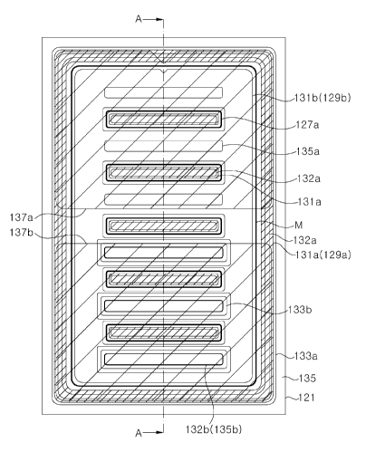
one side and spaced apart from the mesa.
[5] The conventional UV light emitting diode generally has a drawback that
a light output
is low and a forward voltage is high. In
particular, since a p-type GaN layer is included in a
p-type semiconductor layer for an-ohmic contact, ultraviolet light incident
into the p-type
semiconductor layer is absorbed and lost in the p-type semiconductor layer.
In addition,
since an n-ohmic contact layer bonded to an n-type semiconductor layer also
absorbs light,
light traveling into the n-ohmic contact layer is absorbed and lost in the n-
ohmic contact layer.
[6] Furthermore, since it is difficult to use light emitted from a side
surface of the mesa in
the conventional UV light emitting diode, a size of the side surface of the
mesa is set to be
reduced as much as possible. That is,
a width of the mesa is formed to be relatively wide.
However, as the width of the mesa becomes larger, a distance from the n-ohmic
contact layer
to the central region of the mesa becomes farther, and thus, it is not
favorable for current
spreading, and a forward voltage becomes high.
[Disclosure]
[Technical Problem]
[7] Exemplary embodiments provide a deep UV light emitting diode of a novel
structure
capable of improving electrical characteristics, and/or light output.
[8] Exemplary embodiments provide a deep UV light emitting diode capable of
improvi
ng current spreading performance.
[Technical Solution]
[9] A UV light emitting diode according to an exemplary embodiment
includes: a substrate;
an n-type semiconductor layer located on the substrate; a mesa disposed on the
n-type
semiconductor layer, and including an active layer and a p-type semiconductor
layer; n-ohmic
2
Date Recue/Date Received 2021-07-13
CA 03126688 2021-07-13
contact layers in contact with the n-type semiconductor layer; a p-ohmic
contact layer in
contact with the p-type semiconductor layer; an n-bump electrically connected
to the n-ohmic
contact layers; and a p-bump electrically connected to the p-ohmic contact
layer, in which the
mesa includes a plurality of vias exposing a first conductivity type
semiconductor layer, the
mesa has an elongated rectangular shape along a longitudinal direction, the
vias are arranged
parallel to one another in a direction perpendicular to the longitudinal
direction of the mesa,
and the n-ohmic contact layers are formed on the first conductivity type
semiconductor layer
exposed around the mesa and on the first conductivity type semiconductor layer
exposed to the
mesa, respectively.
[10] A UV light emitting diode according to another exemplary embodiment
includes: a
substrate; an n-type semiconductor layer located on the substrate; a mesa
disposed on the n-
type semiconductor layer, and including an active layer and a p-type
semiconductor layer; n-
ohmic contact layers in contact with the n-type semiconductor layer; and a p-
ohmic contact
layer in contact with the p-type semiconductor layer, in which the mesa
includes a plurality of
vias exposing a first conductivity type semiconductor layer, the mesa has an
elongated
rectangular shape along a longitudinal direction, the mesa has a mirror
symmetrical structure
with respect to a plane passing through a center of the mesa along the
longitudinal direction of
the mesa, and in addition, the mesa has a mirror symmetrical structure with
respect to the plane
passing through the center of the mesa along a direction perpendicular to the
longitudinal
direction of the mesa.
[Advantageous Effect]
[11] According to exemplary embodiments of the present disclosure, a large
emission area
may be secured through a mesa having a plurality of vias parallel to one
another in a direction
perpendicular to a longitudinal direction of the mesa, and since a mesa having
a symmetrical
3
Date Recue/Date Received 2021-07-13
CA 03126688 2021-07-13
structure is included, it is possible to provide a deep UV light emitting
diode capable of evenly
spreading current in the mesa.
[12] The advantages and features of the present disclosure will be
discussed in detail in a
detailed description or become apparent through the detailed description.
[Description of Drawings]
[13] FIG. 1 is a plan view illustrating a deep UV light emitting diode
according to an
exemplary embodiment.
[14] FIG. 2 is a cross-sectional view taken along line A-A of FIG. 1.
[15] FIG. 3 is a schematic plan view illustrating a mesa according to an
exemplary
embodiment.
[16] FIG. 4 is a schematic cross-sectional view illustrating a deep UV
light emitting diode
mounted on a sub-mount according to an exemplary embodiment.
[Best Mode]
[17] Hereinafter, embodiments will be described in detail with reference to
the
accompanying drawings. The
following embodiments are provided by way of example so
as to fully convey the spirit of the present disclosure to those skilled in
the art to which the
present disclosure pertains.
Accordingly, the present disclosure is not limited to the
embodiments disclosed herein and can also be implemented in different forms.
In the
drawings, widths, lengths, thicknesses, and the like of devices can be
exaggerated for clarity
and descriptive purposes. When an
element or layer is referred to as being "disposed
above" or "disposed on" another element or layer, it can be directly "disposed
above" or
"disposed on" the other element or layer or intervening devices or layers can
be present.
Throughout the specification, like reference numerals denote like devices
having the same or
4
Date Recue/Date Received 2021-07-13
CA 03126688 2021-07-13
similar functions.
[18] Nitride-based semiconductor layers described below may be grown by
using various
methods commonly known to those skilled in the art, for example, by methods of
Metal
Organic Chemical Vapor Deposition (MOCVD), Molecular Beam Epitaxy (MBE),
Hydride
Vapor Phase Epitaxy (HYPE), or the like. However, in exemplary embodiments
described
below, it is described that semiconductor layers are grown in a growth chamber
using MOCVD.
In growth processes of nitride-based semiconductor layers, for sources flowing
into the growth
chamber, generally known sources may be used. For example, TMGa, TEGa, or the
like
may be used as a Ga source, TMA1, TEAL or the like may be used as an Al
source, TMIn, TEIn,
or the like may be used as an In source, and NH3 may be used as an N source.
However, the
inventive concepts are not limited thereto.
[19] A deep UV light emitting diode according to an exemplary embodiment
includes: a
substrate; an n-type semiconductor layer located on the substrate; a mesa
disposed on the n-
type semiconductor layer, and including an active layer and a p-type
semiconductor layer; n-
ohmic contact layers in contact with the n-type semiconductor layer; a p-ohmic
contact layer
in contact with the p-type semiconductor layer; an n-bump electrically
connected to the n-
ohmic contact layers; and a p-bump electrically connected to the p-ohmic
contact layer, in
which the mesa includes a plurality of vias exposing a first conductivity type
semiconductor
layer, the mesa has an elongated rectangular shape along a longitudinal
direction, the vias are
arranged parallel to one another in a direction perpendicular to the
longitudinal direction of the
mesa, and the n-ohmic contact layers are formed on the first conductivity type
semiconductor
layer exposed around the mesa and on the first conductivity type semiconductor
layer exposed
to the mesa, respectively.
[20] The plurality of vias is formed inside the mesa, and thus, it is
possible to prevent a
Date Recue/Date Received 2021-07-13
CA 03126688 2021-07-13
non-emission region from being formed inside the mesa.
Conventionally, when a width of
the mesa is wide, a distance from the n-ohmic contact layer to the inside of
the mesa increases,
thereby forming a non-emission area. On the
contrary, in the present disclosure, the plurality
of vias is disposed inside the mesa, and the n-ohmic contact layer is formed
in the vias, and
thus, current may be evenly spread inside the mesa.
[21] Meanwhile, the plurality of vias may be spaced apart from one another
at an identical
interval. These
intervals may be adjusted so that the non-emission region is not formed in
the mesa between the vias.
[22] Further, the mesa may have a mirror symmetrical structure with respect
to a plane
passing through a center of the mesa along the longitudinal direction of the
mesa, and in
addition, the mesa may have a mirror symmetrical structure with respect to the
plane passing
through the center of the mesa along the direction perpendicular to the
longitudinal direction
of the mesa.
[23] Since the mesa has the symmetrical structure, it is possible to
prevent current from
being concentrated through a particular location of the mesa.
[24] Meanwhile, the interval between the vias may be equal to or greater
than the interval
between one end of the via and one edge of the mesa. In
addition, an interval between a
short edge of the mesa and the via may be equal to or greater than the
interval between the vias.
[25] Meanwhile, the n-ohmic contact layer disposed on the first
conductivity type
semiconductor layer exposed around the mesa may surround the mesa. As such,
current may
be evenly spread over an entire region of the mesa.
[26] Meanwhile, the deep UV light emitting diode may further include n-
capping layers
and a p-capping layer covering the n-ohmic contact layers and the p-ohmic
contact layer,
respectively, in which the capping layers may cover upper and side surfaces of
the ohmic
6
Date Recue/Date Received 2021-07-13
CA 03126688 2021-07-13
contact layers.
[27] The deep UV light emitting diode may further include: a lower
insulation layer
covering the mesa, the n-ohmic contact layers, and the p-ohmic contact layer,
and having
openings located over the n-ohmic contact layers and the p-ohmic contact
layer; an n-pad metal
layer and a p-pad metal layer disposed on the lower insulation layer, and
electrically connected
to the n-ohmic contact layers and the p-ohmic contact layer through the
openings of the lower
insulation layer, respectively; and an upper insulation layer covering the n-
pad metal layer and
the p-pad metal layer, in which the n-bump and the p-bump may be disposed on
the upper
insulation layer, and electrically contact the n-pad metal layer and the p-pad
metal layer through
openings of the upper insulation layer.
[28] Further, the n-pad metal layer may include a reflective metal layer,
for example, an Al
layer.
[29] In addition, the n-pad metal layer may reflect light emitted through a
side surface of
the mesa. As such,
light emitted through the side surface of the mesa and lost may be
reduced, and thus, the light efficiency of the deep UV light emitting diode
may be improved.
[30] The deep UV light emitting diode may further include n-capping layers
and a p-
capping layer covering the n-ohmic contact layers and the p-ohmic contact
layer, respectively,
in which the n-pad metal layer may be connected to the n-capping layers to be
electrically
connected to the n-ohmic contact layers.
[31] Further, the n-capping layers may include a reflective metal layer,
for example, an Al
layer. As such,
it is possible to reflect light emitted from the n-type semiconductor layer
using the n-capping layer, and thus, the light efficiency of the deep UV light
emitting diode
may be improved.
[32] In an exemplary embodiment, the n-pad metal layer may surround the p-
pad metal
7
Date Recue/Date Received 2021-07-13
CA 03126688 2021-07-13
layer. However, the inventive concepts are not necessarily limited thereto.
[33] A deep UV light emitting diode according to another exemplary
embodiment includes:
a substrate; an n-type semiconductor layer located on the substrate; a mesa
disposed on the n-
type semiconductor layer, and including an active layer and a p-type
semiconductor layer; n-
ohmic contact layers in contact with the n-type semiconductor layer; and a p-
ohmic contact
layer in contact with the p-type semiconductor layer, in which the mesa
includes a plurality of
vias exposing a first conductivity type semiconductor layer, the mesa has an
elongated
rectangular shape along a longitudinal direction, the mesa has a mirror
symmetrical structure
with respect to a plane passing through a center of the mesa along the
longitudinal direction of
the mesa, and in addition, the mesa has a mirror symmetrical structure with
respect to the plane
passing through the center of the mesa along a direction perpendicular to the
longitudinal
direction of the mesa.
[34] Since the mesa has the symmetrical structure, it is possible to
prevent current from
being concentrated through a particular location of the mesa, and thus, the
deep UV light
emitting diode capable of evenly spreading current inside the mesa may be
provided.
[35] The vias may have an elongated shape along the direction perpendicular
to the
longitudinal direction of the mesa, and may be arranged parallel to one
another. The vias
are formed in the elongated shape, and thus, current may be evenly spread not
only in a region
between the vias but also in a region between the via and an edge of the mesa.
[36] Meanwhile, the n-ohmic contact layers may include an n-ohmic contact
layer
surrounding the mesa and n-ohmic contact layers disposed in the vias.
[37] Meanwhile, the deep UV light emitting diode may further include an n-
pad metal layer
electrically connected to the n-ohmic contact layers; and p-pad metal layers
electrically
connected to the p-ohmic contact layer, in which the n-pad metal layer may
surround the p-pad
8
Date Recue/Date Received 2021-07-13
CA 03126688 2021-07-13
metal layers.
[38] The n-pad metal layer and the p-pad metal layers may be formed through
an identical
process to be located at an identical level.
[39] The deep UV light emitting diode may further include a lower
insulation layer covering
the mesa, the n-ohmic contact layers, and the p-ohmic contact layer, in which
the n-pad metal
layer and the p-pad metal layers may be disposed on the lower insulation
layer, and may be
electrically connected to the n-ohmic contact layers and the p-ohmic contact
layer through
openings formed in the lower insulation layer, respectively.
[40] Further, the deep UV light emitting diode may further include an upper
insulation layer
covering the n-pad metal layer and the p-pad metal layers; and an n-bump and a
p-bump
disposed on the upper insulation layer, in which the n-bump may be
electrically connected to
the n-pad metal layer, and the p-bump may be electrically connected to the p-
pad metal layers.
[41] Hereinafter, exemplary embodiments of the present disclosure will be
described in
detail with reference to the drawings.
[42] FIG. 1 is a schematic plan view illustrating a deep UV light emitting
diode according
to an exemplary embodiment, and FIG. 2 is a cross-sectional view taken along
line A-A of FIG.
1. Meanwhile, FIG. 3 is a schematic plan view illustrating a mesa according
to an exemplary
embodiment.
[43] Referring to FIGS. 1, 2, and 3, the UV light emitting diode according
to the exemplary
embodiment may include a substrate 121, an n-type semiconductor layer 123, an
active layer
125, a p-type semiconductor layer 127, an n-ohmic contact layer 129a, a p-
ohmic contact layer
129b, an n-capping layer 131a, a p-capping layer 131b, a lower insulation
layer 132, an n-pad
metal layer 133a, a p-pad metal layer 133b, an upper insulation layer 135, an
n-bump 137a and
9
Date Recue/Date Received 2021-07-13
CA 03126688 2021-07-13
a p-bump 137b, and an anti-reflection layer 139.
[44] The substrate 121 is not limited as long as it is a substrate capable
of growing a nitride-
based semiconductor, for example, and it may include a heterogeneous substrate
such as a
sapphire substrate, a silicon substrate, a silicon carbide substrate, a spinet
substrate or the like,
or it may include a homogeneous substrate such as a gallium nitride substrate,
an aluminum
nitride substrate, or the like.
[45] The n-
type semiconductor layer 123 is disposed on the substrate 121. The n-type
semiconductor layer 123 may include, for example, an AIN buffer layer (about
3.79 pin) and
an n-type AlGaN layer. The n-type AlGaN layer may include a lower n-type AlGaN
layer
(about 2.15 pin) having a mole ratio of Al of 0.8 or more, an intermediate
AlGaN layer (1.7
nm) having an Al mole ratio of 0. 7 to 0.8, and an upper n-type AlGaN layer
having a thickness
of 66.5 nm. The n-
type semiconductor layer 123 is formed of a nitride-based semiconductor
having a band gap wider than that of an active layer so as to transmit light
generated in the
active layer. In a
case where a gallium nitride based semiconductor layer is grown on a
sapphire substrate 121, the n type semiconductor layer 123 may usually include
a plurality of
layers so as to improve crystalline quality.
[46] The mesa M is disposed on a partial region of the n-type semiconductor
layer 123.
The mesa M includes the active layer 125 and the p-type semiconductor layer
127. In general,
after the n-type semiconductor layer 123, the active layer 125, and the p-type
semiconductor
layer 127 are sequentially grown, the mesa M is formed by patterning the p-
type semiconductor
layer 127 and the active layer 125 through a mesa etching process.
[47] The active layer 125 may be a single quantum well structure or a
multiple quantum
well structure including well layers and barrier layers. The well layers may
be formed of
AlGaN or AlInGaN, and the barrier layers may be formed of AlGaN or AlInGaN
having a
Date Recue/Date Received 2021-07-13
CA 03126688 2021-07-13
wider band gap than that of the well layer. For example, each well layer may
be formed of
AlGaN having a mole ratio of Al of about 0.5 with a thickness of about 3.1 nm,
and each barrier
layer may be formed of AlGaN having a mole ratio of Al of 0.7 or more with a
thickness of
about 9 nm or more. In particular, a first barrier layer may be formed thicker
than the
remaining barrier layers with a thickness of about 12 nm or more. Meanwhile,
AlGaN layers
having an Al mole ratio of 0.7 to 0.8 may be disposed in contact with upper
and lower portions
of each well layer with a thickness of about 1 nm, respectively. However, an
Al mole ratio of
the AlGaN layer contacting a last well layer may be 0.8 or more in
consideration of contacting
an electron blocking layer.
[48] Meanwhile, the p-type semiconductor layer 127 may include an electron
blocking
layer and a p-type GaN contact layer. The electron blocking layer prevents
electrons from
overflowing from the active layer to the p-type semiconductor layer, and thus,
recombination
rate of electrons and holes is improved. The electron blocking layer may be
formed of, for
example, p-type AlGaN having a mole ratio of Al of about 0. 8, and may be
formed with a
thickness of, for example, 55 nm. Meanwhile, the p-type GaN contact layer may
be formed
to have a thickness of about 300 nm.
[49] As illustrated in FIG. 3, the mesa M may have an elongated rectangular
shape in one
direction, and includes a plurality of vias 127a exposing the n-type
semiconductor layer 123.
Each of the vias 127a may have an elongated shape, and may be disposed in a
direction
perpendicular to a longitudinal direction of the mesa M. The vias 127a may be
spaced apart
from one another and arranged in parallel, and further, the vias 127a may be
spaced apart from
one another at an identical interval sl. Meanwhile, an interval s2 between one
end of the via
127a in the longitudinal direction and an edge of the mesa M adjacent thereto
may be equal to
or less than the interval sl between the vias 127a. In addition, an interval
s3 between a short
11
Date Recue/Date Received 2021-07-13
CA 03126688 2021-07-13
edge of the mesa M and the via 127a adjacent thereto may be equal to or
greater than the
interval sl between the vias 127a.
[50] Furthermore, the mesa M may have a mirror symmetrical structure with
respect to a
plane crossing a center of the mesa along the longitudinal direction of the
mesa, and in addition,
may also have a mirror symmetrical structure with respect to the plane
crossing the center of
the mesa along a direction perpendicular to the longitudinal direction of the
mesa. With this
shape, current may be evenly spread in the mesa M.
[51] Referring back to FIGS. 1 and 2, the n-ohmic contact layers 129a are
disposed on the
n-type semiconductor layer 123 exposed around the mesa M and exposed to the
vias 127a.
After a plurality of metal layers is deposited, the n-ohmic contact layers
129a may be formed
by alloying these metal layers through a rapid thermal alloy (RTA) process.
For example, the
n-ohmic contact layer 129a may be formed by after sequentially depositing
Cr/Ti /Al /Ti /Au,
and alloying these metal layers through the RTA process. As such, the n-ohmic
contact layer
129a becomes an alloy layer containing Cr, Ti, Al, and Au.
[52] An n-ohmic contact layer 129a surrounds the mesa M along a periphery
of the mesa
M. In addition, the n-ohmic contact layers 129a are disposed in the vias
127a. .. A width wl
of the n-ohmic contact layer 129a surrounding the mesa M along the periphery
of the mesa M
may be smaller than a width w2 of the n-ohmic contact layer 129a disposed in
the via 127a.
Since the width w2 of the n-ohmic contact layer 129a disposed in the via 127a
is set to be larger
than the width wl of the n-ohmic contact layer around the mesa, current may be
easily supplied
into the mesa M. The width wl may be in a range of about 5 pm to 30 pm, for
example, and
the width w2 may be in a range of about 10 pm to 40 pm.
[53] The n-ohmic contact layers 129a are spaced apart from the mesa M at a
predetermined
interval.
Accordingly, a region without the n-ohmic contact layer 129a is formed between
12
Date Recue/Date Received 2021-07-13
CA 03126688 2021-07-13
the mesa M and the n-ohmic contact layer 129a. A separation distance between
the n-ohmic
contact layer 129a and the mesa M may be constant along the periphery of the
mesa M, but the
inventive concepts are not necessarily limited thereto.
[54] After
the n-ohmic contact layers 129a are formed, the p-ohmic contact layer 129b is
formed on the mesa M. The p-ohmic contact layer 129b may be formed through the
RTA
process after depositing Ni/Au, for example. The p-
ohmic contact layer 129b is in ohmic
contact with the p-type semiconductor layer 127 and covers most of, for
example, 80% or more
of an upper region of the mesa M.
[55] The n-capping layers 131a and the p-capping layer 131b may be formed
on the n-
ohmic contact layers 129a and the p-ohmic contact layer 129b, respectively.
The n and p-
capping layers 131a and 131b may cover upper and side surfaces of the n-ohmic
contact layers
129a and the p-ohmic contact layer 129b. These
capping layers 131a and 131b may include
a reflective metal layer, for example, an Al layer, and specifically, may be
formed of
Cr/Al/Ti/Ni/Ti/Ni/Ti/Ni/Au/Ti. In
particular, the n-capping layer 131a may have a larger
width than that of the n-ohmic contact layer 129a, and thus, may function as a
reflection layer
(first reflection layer) that reflects light emitted through the n-type
semiconductor layer 123.
Further, the n-capping layer 131a may have an elevation lower than that of the
mesa M, and
thus, an upper surface of the n-capping layer 131a may be located below an
upper surface of
the mesa M.
[56] The lower insulation layer 132 covers the mesa M, and in addition,
covers the n-
capping layers 131a and the p-capping layer 131b. The
lower insulation layer 132 also
covers the n-type semiconductor layer 123 exposed around the mesa M and
exposed in the vias
127a.
Meanwhile, the lower insulation layer 132 has openings 132a for allowing
electrical
connection to the n-ohmic contact layers 129a and openings 132b for allowing
electrical
13
Date Recue/Date Received 2021-07-13
CA 03126688 2021-07-13
connection to the p-ohmic contact layer 129b. The openings 132a and 132b
exposing the
capping layers 131a and 131b may be formed by etching the lower insulation
layer 132. In
this case, a Ti layer on upper surfaces of the exposed capping layers 131a and
131b may be
removed by the etching process.
[57] The lower insulation layer 132 may be formed of, for example, SiO2,
but the inventive
concepts are not limited thereto, and may be formed of a distributed Bragg
reflector.
[58] Meanwhile, the n-pad metal layer 133a and the p-pad metal layer 133b
are disposed
on the lower insulation layer 132. The n-
pad metal layer 133a and the p-pad metal layer
133b may be formed together using an identical metal layer in an identical
process and may be
disposed on an identical level, that is, on the lower insulation layer 132.
The n and p-pad
metal layers 133a and 133b may include a reflective metal layer, for example,
an Al layer so as
to have high reflectivity. For
example, then and p-pad metal layers 133a and 133b may have
an identical layer structure as that of the capping layers 131a and 131b.
[59] The n-pad metal layer 133a is electrically connected to the n-ohmic
contact layers 129a
through the openings 132a of the lower insulation layer 132. The n-ohmic
contact layers 129a
are electrically connected to one another by the n-pad metal layer 133a. The n-
pad metal
layer 133a may extend to the upper region of the mesa M from the n-ohmic
contact layers 129a
located below the mesa M.
[60] The p-pad metal layers 133b may be electrically connected to the p-
ohmic contact
layer 129b through the openings 132b of the lower insulation layer 132,
respectively. The
p-pad metal layers 133b are spaced apart from one another, and may be
surrounded by the n-
pad metal layer 133a, respectively.
[61] The n-pad metal layer 133a may function as a reflection layer (second
reflection layer)
that reflects light emitted through a side surface of the mesa M, thereby
improving the light
14
Date Recue/Date Received 2021-07-13
CA 03126688 2021-07-13
efficiency of the light emitting diode. In addition, the n-capping layers 131a
and the n-pad
metal layer 133a may reflect light emitted from the n-type semiconductor layer
123 exposed in
a region between the mesa M and the n-ohmic contact layers 129a.
[62] The
upper insulation layer 135 covers the n-pad metal layer 133a and the p-pad
metal
layers 133b. However,
the upper insulation layer 135 has openings 135a exposing the n-pad
metal layer 133a and openings 135b exposing the p-pad metal layers 133b in the
upper region
of the mesa M. The opening 135a may be formed to have an elongated shape along
the via
127a. As shown
in the drawing, the openings 135a may be disposed above a line passing
through the center of the mesa along a short axis direction of the mesa M.
Meanwhile, the
openings 135b may be disposed below the line passing through the center of the
mesa along
the short axis direction of the mesa M. The
upper insulation layer 135 may be formed of,
for example, silicon nitride or silicon oxide.
[63] The n-
bumps 137a and p-bumps 137b are located on the upper insulation layer 135.
The n-bump 137a covers the opening 135a and is connected to the n-pad metal
layer 133a
through the opening 135a. The n-
bump 137a is electrically connected to the n-type
semiconductor layer 123 through the n-pad metal layer 133a and the n-ohmic
contact layers
129a. Outer edges of the n-bumps 137a and p-bumps 137b may be located on the n-
ohmic
contact layer 129a surrounding the mesa M.
[64] The p-
bump 137b covers the openings 135b and is connected to the p-pad metal layers
133b through the openings 135b. The p-
bump 137b is electrically connected to the p-type
semiconductor layer 127 through the p-pad metal layers 133b and the p-ohmic
contact layer
129b. The p-
pad metal layers 133b may be electrically connected to one another through
the p-bump 137b.
[65] The n-
bumps 137a and p-bumps 137b may be formed of, for example, Ti/Au/Cr/Au.
Date Recue/Date Received 2021-07-13
CA 03126688 2021-07-13
As shown in FIG. 1, the n-bumps 137a and the p-bumps 137b may be disposed
along the
longitudinal direction of the mesa M. The n-bumps 137a and the p-bumps 137b
may be
spaced apart by about 90 nm. Since an
interval between the n-bumps 137a and the p-bumps
137b is set to be narrow, areas of the n-bumps 137a and the p-bumps 137b may
be relatively
widened. As such, it is possible to easily dissipate heat generated in the
light emitting diode,
and thus, performance of the light emitting diode may be improved.
[66] Further, the openings 135a and 135b are covered with the n-bumps 137a
and the p-
bumps 137b, and thus, moisture or solder from the outside may be prevented
from penetrating
through the openings 135a and 135b, thereby improving reliability of the light
emitting diode.
[67] Meanwhile, as shown in FIG. 2, upper surfaces of the n-bumps 137a and
p-bumps
137b may not be flat due to a difference in elevation between the mesa M and
the n-pad metal
layer 133a.
[68] The anti-reflection layer 139 is disposed on alight exiting surface of
the substrate 121.
The anti-reflection layer 139 may be formed of a transparent insulation layer
such as 5i02 with
a thickness of an integer multiple of 1/4 of an ultraviolet wavelength, for
example.
Alternatively, as the anti-reflection layer 139, a bandpass filter in which
layers having different
refractive indices from one another are repeatedly stacked may be used.
[69] FIG. 4 is a schematic cross-sectional view illustrating a deep UV
light emitting diode
mounted on a sub-mount according to an exemplary embodiment.
[70] Referring to FIG. 4, the deep UV light emitting diode is flip-bonded
on a sub-mount
substrate 200. The sub-
mount substrate 200 may have electrode pads 201a and 201b on an
insulating substrate such as AIN.
[71] N-bumps 137a and p-bumps 137b may be bonded to the electrode pads 201a
and 201b
of the sub-mount substrate 200 through solder pastes 203a and 203b.
However, the inventive
16
Date Recue/Date Received 2021-07-13
CA 03126688 2021-07-13
concepts are not limited thereto, and the deep UV light emitting diode may be
bonded to the
sub-mount substrate 200 using thermal ultrasonic bonding technology or solder
bonding using
AuSN.
[72] Various
modifications and changes can be made in the exemplary embodiments descr
ibed herein without departing from the technical spirit according to the
appended claims of th
e present disclosure, and the present disclosure comprises all the technical
ideas according to
the appended claims.
17
Date Recue/Date Received 2021-07-13