Note: Descriptions are shown in the official language in which they were submitted.
CA 03127498 2021-07-21
WO 2020/163434
PCT/US2020/016725
ALUMINUM NITRIDE HEATER AND METHODS OF MAKING SAME
Field of the Invention
The present disclosure relates to a heater for a variety of uses. The heater
defines an
essentially pure aluminum nitride base having thick film printing, including
resistive and
conductive layers and overlayers of glass.
Background
Heaters have many and diverse applications in the industries of automotive
vehicles,
appliances, and consumer items, to name a few. They serve as cabin heaters in
electric and hybrid
vehicles, water heaters for dishwashers and washing machines, and sources of
heat for hair
dryers/straighteners, cooking apparatuses, and space heaters, etc. In imaging
devices, such as
printers and copiers, heaters exist in fusers to melt and fix toner on media.
However, when narrow
media (e.g., envelopes) are imaged, portions of the fusers extending beyond
the media quickly
overheat due to low thermal mass components which can become damaged. Some
printers having
a belt fuser heated by an aluminum oxide, thick-film printed, ceramic heater
slow from 70 pages-
per-minute print speed for full-sized media to 7 ppm for narrow media to
prevent fuser damage by
better controlling temperature, but at the expense of printing speed.
Positive Temperature Coefficient (PTC) heaters have been tested as a means of
preventing
damage to fusers during printing of narrow media. Some have suggested that PTC
heaters are
desirable for 2 main reasons: 1) PTC materials have a Curie point in a
temperature region that can
.. eliminate damage to other components, theoretically allowing narrow media
to be printed at higher
speeds than occurs with aluminum oxide heaters; and 2) the lower Curie point
of the PTC materials
serves as a safety feature. However, the inventors note that PTC materials
alone are not
advantageous because they have relatively low thermal conductivity. For PTC
materials to be
more effective, heat must be dissipated quickly from the PTC materials.
Furthermore, PTC
materials, when cold, have a severely low resistance - creating an extremely
high in-rush current.
An aluminum nitride substrate, thick film heater, has been also mentioned for
preventing
damage to fusers during printing of narrow media. However, aluminum nitride
heaters to date
have been limited to hybrids consisting of about 80% aluminum nitride and
about 20% aluminum
oxide. Such materials have a thermal conductivity of about 80W/mK compared to
aluminum oxide
1
CA 03127498 2021-07-21
WO 2020/163434
PCT/US2020/016725
which has a thermal conductivity of about 23 W/mK. Thus, the inventors propose
an essentially
pure aluminum nitride substrate, thick film heater, having a significantly
higher thermal
conductivity with a thermal conductivity of about 200 W/mK. No one as of yet,
however, has
been able to successfully thick-film print a large area resistor heater on
such a substrate without
Kirkendall voids (e.g., voids or gaps between the thick-film printed conductor
and resistor layers
on the substrate). In turn, voids such as these lead to extremely high
electrical resistance causing
heater failure. Furthermore, existing glass pastes cannot be used for thick-
film printing di-electric
glasses or cover glasses serving as electrical insulation layers over the
conductor and resistor layers
due to large voids in the glass. The inventors identify one reason for this as
current manufacturing
processes have difficulty in out-gassing nitrogen gas during high temperature
firing/heating
(typically 850 C) of the substrate having the conductor, resistor, and glass
paste materials.
A need exists to overcome the foregoing. The inventors further note that any
solutions in
the technology of heaters should further contemplate the competing design
constraints found in
power consumption, safety features, warm-up characteristics, operating
temperatures, heating
speeds, thermal conductivity, materials, costs, electrical requirements,
construction, materials to-
be-heated, temperature control, installation/integration with other
components, size, shape, and
dimensions, and the like.
Summary
A heater includes an aluminum nitride base having equal to or less than 1%
impurities,
especially none of polybrominated biphenyl (PBB), polybrominated diphenyl
ether (PBDE),
hexabromocyclododecane (HBCDD), polyvinyl chloride (PVC), chlorinated
paraffin, phthalate,
cadmium, hexavalent chromium, lead, and mercury. At least one longitudinally
extending
resistive trace of silver and palladium overlies the base as does a conductor
of silver and platinum
or silver and palladium that electrically connects to the resistive trace to
apply an external voltage
to the resistive trace for heating thereof At least four, but optionally five
layers of glass overlie
the resistive trace and conductor, but not an entirety of the conductor. A
first two consecutive
layers of the glass layers define a first glass having a solid content of more
than 65% and a viscosity
of 100 Pa = s or less. The following two or three consecutive layers of the
five layers define a
second glass dissimilar to the first.
2
CA 03127498 2021-07-21
WO 2020/163434
PCT/US2020/016725
A method of making a heater includes thick film printing an aluminum nitride
base having
equal to or less than 1% impurities. The base is fired in a heating unit
before any layering of the
base. Thereafter, on a topside and backside of the base a conductor layer from
a conductive paste
is layered and allowed to settle and dry before firing the base having the
conductor layers. Next,
a resistive layer is layered on the base from a resistor paste such that the
resistive layer connects
to the conductor layer on the topside of the base. The resistor paste is
allowed to settle and dry
and then the base with the conductor and resistor layers is fired in the
heating unit. At least four
layers of glass are layered next over the resistive layer. Each instance
thereof includes layering a
glass, drying the glass and firing the base including the glass so layered.
Settling, drying, and
firing profiles are also noted under various embodiments.
The embodiments noted herein eliminate life-limiting Kirkendall voids in thick
film
printing of silver platinum (AgPt) conductors and silver palladium (AgPd)
resistors at the interface
of the conductor and resistor layers. The embodiments also eliminate large,
prohibitive voids in
layers of glass.
Further embodiments teach blends of resistor paste of about 80% silver and
about 20%
palladium for thick film printing on an aluminum nitride base, but still
supporting a 115 volt
resistor. The embodiments pioneer the use of relatively low palladium content
unlike typical prior
pastes of about 45% silver and 55% palladium. Pastes for conductor layers
include content of
about 93% silver and about 7% palladium or platinum and being essentially free
of Kirkendall
voids at the juncture of the resistor to conductor. The embodiments overcome
problems noted
with typical prior conductive pastes.
Still further embodiments note the use of a relative low firing temperature
for a thick film
di-electric ("cross glass") and a cover glass overlying the resistor and
conductive layers. As has
been practiced in the past, typical large area ceramic heaters utilized a
glass firing temperature of
approximately 850 C. Whereas, embodiments of the present disclosure separate
the "cross glass"
(higher di-electric properties) from a cover glass (lower di-electric
properties but improved surface
quality) and fire the cross glass at a peak temperature as low as about 835 C
while the cover glass
could be fired as low as about 810 C. Without being bound by theory, the
lower firing
temperatures are believed to be fundamental to preventing large voids in any
of the glass layers
(leading to poor di-electric strength) and guaranteeing no Kirkendall voids
between the resistive
3
CA 03127498 2021-07-21
WO 2020/163434
PCT/US2020/016725
and conductive layers. The inventors also found the lower temperatures of
firing the glass helped
in two ways. First, silver migration was diminished between the silver content
of each of the
resistor and conductor material. Second, the oxidation of the palladium in the
resistor and
conductor materials was lowered in those embodiments containing palladium,
where palladium
.. oxidation and reduction rates are known to relate to Kirkendall voids.
In even further embodiments, oxidizing or plasma treating the surface of the
aluminum
nitride base further contributes to eliminating the deleterious effects of
nitrogen out-gassing during
later instances of firing the base which occurs during print, dry, and firing
sequences of thick film
printing.
The embodiments of the invention support many forms of heaters for use in many
and
diverse applications. In one design, the heater is contemplated for use as a
cabin heater for Electric
Vehicles (EV) and hybrid vehicles. Traditional cabin heaters today utilize a
series of PTC heaters
embedded in a radiator type arrangement, i.e. an array of aluminum finned heat
spreaders attached
to PTC heaters. Air flows through the aluminum fin heat spreaders - removing
heat from the PTC.
.. However, a major disadvantage of a PTC heater (only) arrangement is that it
heats relatively
slowly. Auto users complain about the relatively slow warm-up time of the PTC
only cabin heaters
which is attributed to a relatively high in-rush of current. Developers then
must be careful not to
drain the battery of the vehicle or use excessive fuel to handle the excessive
in-rush current. With
the embodiments of the present heater, however, the essentially pure aluminum
nitride heater
supports thermal conductivity of about 200 W/mK and can serve as both a pre-
heater and heat
spreader to the PTC heater array - eliminating any slow warm-up of cabin
heaters. It also supports
power designs of about 1200 Watts or more.
In other applications, an essentially pure aluminum nitride heater facilitates
the printing of
narrow media in an imaging device without the problems of the prior art and
can bear the duties
of warming up a belt and back-up roller in a belt fuser in imaging devices.
Such a heater can also
pre-heat a series of PTC elements and then be turned off Heating of the PTC
can commence until
the in-rush current is within 10% - 20%, for example, of the steady state
current. Such a dual
combination heating scheme allows for much quicker warm-up times.
4
CA 03127498 2021-07-21
WO 2020/163434
PCT/US2020/016725
Brief Description of the Figures:
Fig. 1A is an exploded view of an aluminum nitride heater according to a
representative
embodiment of the present invention;
Fig. 1B is a non-exploded view of the aluminum nitride heater of Fig. 1A;
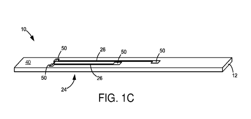
Fig. 1C is a backside view of the aluminum nitride heater of Fig. 1B;
Figs. 2A-2F are diagrammatic views of a representative sequence of printing,
drying and
firing layers on a substrate when forming an aluminum nitride heater;
Figs. 3A-3E are diagrammatic views of a representative sequence of printing
and drying
layers on a substrate when forming an aluminum nitride heater;
Figs. 4A and 4B are diagrammatic views of a representative sequence of only
firing a
substrate with an optional layer(s) when forming an aluminum nitride heater;
Figs. 5A-5E are diagrammatic views of a representative sequence of printing,
drying and
firing patterned layers on a substrate, such as resistive traces and
conductors, when forming an
aluminum nitride heater;
Figs. 6A-6I are diagrammatic planar views of a representative sequence of
patterning a
plurality of top layers on a base forming an aluminum nitride heater;
Fig. 7 is a diagrammatic view of a large substrate for dicing into plural,
individual
aluminum nitride heaters; and
Figure 8 is a graph of a representative heating profile according to
embodiments of the
invention for firing in a heating unit a base or substrate with or without
overlying layers.
Detailed Description
Figures 1A and 1B teach a heater 10 for a variety of uses. The heater includes
an essentially
pure aluminum nitride base or substrate 12. Essentially pure is at least 5%
impurities or less, but
equal to or less than 1% is preferred. In one embodiment, the impurities of
the base do not include
any of polybrominated biphenyl (PBB), polybrominated diphenyl ether (PBDE),
hexabromocyclododecane (HBCDD), polyvinyl chloride (PVC), chlorinated
paraffin, phthalate,
cadmium, hexavalent chromium, lead, and mercury. The shape of the base
includes a
5
CA 03127498 2021-07-21
WO 2020/163434
PCT/US2020/016725
longitudinally extending solid of a generally rectangular shape having a
length (1) and width (w)
dimension and a thickness (t). After separating by dicing in Figure 7 from a
saw 15 along dashed
lines 17 and 19 from a larger wafer 20, for example, representative dimensions
of each heater 10
include a thickness in a range of about 0.5 ¨0.7 mm, a length in a range of
about 150¨ 160 mm,
.. and a width in a range of about 6 ¨ 8 mm.
With continued reference to Figures lA and 1B, each heater 10 includes at
least one
resistive trace 22 on a topside 24 of the base. Connected to each resistive
trace at interface 25 is a
conductor 26. During use, the conductor 26 receives power from an external
voltage source to
power the resistive trace(s) 22. In turn, the resistive trace heats and
provides heating to the device
in which it is used, such as for a cabin heater in an electric or hybrid
vehicle or a fuser in an imaging
device. In one embodiment, the external source is 115 VAC. In others, it is
12VDC, 350 VDC,
650 VDC or 800 VDC. In any, the resistive trace and conductor support the
voltage and lack
Kirkendall voids at the interface 25, by way of the methods of manufacturing
the heater as
described below. In dimensions, the thickness of the resistive trace is about
10 ¨ 13 p.m on the
aluminum nitride base and has a length of about 135 ¨ 145 mm and a width of
about 4.5 ¨ 5.5 mm.
The conductor has a thickness of about 9 ¨ 15 p.m on the aluminum nitride
base, a length of about
11 ¨ 13 mm, and a width of about 4.8 ¨ 5.8 mm. Also, the resistive trace has a
resistance of about
10 ¨ 12 ohms at 195 C. The resistive trace is formed from a resistor paste of
about 80% silver
and 20% palladium while the conductor is formed from a conductive paste of
silver and palladium
or platinum. In one embodiment, pastes for conductor layers include content of
about 93% silver
and about 7% palladium or platinum.
Overlying each resistive trace and at least a portion of the conductor, but
not an entirety of
the conductor as it needs to connect to the external power source, is at least
four layers of glass 30
(30-1, 30-2, 30-3, 30-4, Figure la). The glass is any of a variety but the
first two consecutive glass
layers 30-1, 30-2 are of a first type, while the next two 30-3, 30-4 are of a
different type. The first
type defines a cross glass layer, while the different type defines a cover
glass layer. Any of the
four glass layers define a glass having a viscosity of 100 Pa = s or less.
More particularly, the
viscosity exists at 90 Pa = s or less, especially 65 Pa = s or less. Its solid
content, on the other hand,
exists at 65% or more. In various specific embodiments, the glass is purchased
commercially from
AGC, Inc. (formerly the Asahi Glass Company) as seen in Table 1. Its
properties are also noted.
6
CA 03127498 2021-07-21
WO 2020/163434
PCT/US2020/016725
Table 1
AGC, Inc. Thixotropic Index Viscosity (Pa = s) Solid
Content (%)
Glass Paste ID
AP5717B10 2.0 ¨ 2.4 100 66
AP5717B13 1.6 89 69
AP5717B14 1.4 61 72
In any layer of glass, the dimensions include a thickness in a range of about
10 ¨ 13 p.m
on the aluminum nitride base, a length in a range of about 135 ¨ 145 mm, and a
width in a range
of about 4.5 ¨5.5 mm. In one embodiment, the first two consecutive layers 30-
1, 30-2 of the at
least four glass layers together have a thickness of about 24 p.m. The next
two consecutive layers
30-3, 30-4 and a fifth layer of glass (not shown until Figure 61) together
have a combined thickness
of about 65 p.m. The fifth layer of glass also overlies the base and resistive
and conductive layers
and is similar in composition to any of the cover glass layers.
With reference to Figure 1C, a bottom or backside 40 of the base 12 optionally
includes
one or more thermistors 50. They interconnect with a same or different
conductor 26 of the
topside. They are positioned to measure the temperature of the heater 10 and
the conductor 26
connects the thermistors to external sources to measure, store and control the
temperature.
With reference to the Figure sets of 2A et seq., 3A et seq., and 4A et seq.,
the general
process steps for fabricating the heater 10 of Figures la and lb will be
described. They include
one or more of thick-film printing, settling, drying, and firing or heating.
As shorthand from the
industry, they are generally known as print, dry, and fire, or PDF.
In more detail, the Figures 2A-2F show printing, drying, and firing. In Figure
2A, a base
or substrate, such as the essentially pure aluminum nitride base 12, is
provided. In Figure 2B,
thick-film printing of the substrate includes providing a mesh stencil 60 upon
and through which
a paste 62 is applied. In the instance of layering a resistor, conductor or
glass, a resistive paste, a
conductive paste or a glass paste is applied. In Figure 2C, a leveling device
64, such as a squeegee
or other scraper, levels the paste on a surface 66 (Figure 2B) of the base. In
Figure 2D, the paste
7
CA 03127498 2021-07-21
WO 2020/163434
PCT/US2020/016725
so applied is allowed to settle on the base forming a layer 70 upon removal of
the stencil. This
settling occurs typically for about five to ten minutes at room temperature,
e.g., 20 - 25 C. In
Figure 2E, the base and layer is provided to a curing or drying unit 80. The
drying unit typifies a
box oven or blast furnace and the base is provided to the unit along a
conveyor, typically. The
drying unit begins drying the layer 70 at around room temperature followed by
a curing or drying
cycle of about 30 minutes reaching temperatures of 140 - 160 C. In one
embodiment, the drying
cycle includes applying infrared heat or hot air (both given generically as
heat 82) for a period of
time of about 30 total minutes at a temperature profile of the drying unit
beginning at about 25 C
and ramping up to about 80 C for about 10 minutes, ramping up again to about
160 C for about
10 minutes and cooling down to below 50 C. After that, the base 12 with layer
70 is fired in a
heater or firing unit 80'. In some instances, the firing unit 80' is the same
unit as the drying unit
80, but having different heating profiles. In others, the firing unit 80' is
different from the drying
unit 80 and the base advances from one unit to the next along a conveyor,
typically. In any, the
heating profile for heating the base depends upon which type of layer is most
recently printed and
dried thereon, e.g., resistive layer, conductive layer or glass layer.
In Figure 8, a representative heating profile for any layer is shown in graph
100. Namely.
the heating profile for a un-layered base or resistive or conductive layer is
shown by the solid line
102, whereas a dashed line 104 depicts the heating profile for glass. In
general, the heating profile
of the heating unit includes a total heating time of about 40 total minutes
starting at about 25 C
and ramping up to a peak temperature (part of zones 5-8) by 20 minutes and
maintaining the peak
temperature for at least 10 minutes and decreasing the temperature of the
heating unit (post zone
8) for at least 10 minutes thereafter. Cooling continues even further
thereafter (post zone 12) until
completely cooled. For an un-layered base or the resistive or conductive
layers, the peak
temperature reaches about 850 C. The glass layers, on the other hand, have a
peak temperature
of 830 C or 810 C, depending on which layers. Table 2, infra, provides a
representative
embodiment of which glass layers heat at which temperatures.
With reference to Figures 3A-3E, instances are shown of thick-film printing a
base 12 to
form and dry a layer 12 thereon. The views are similar to Figures 2A-2E,
except there is no
instance of firing the base/layer(s) in a firing unit. Rather, the processing
steps only include
8
CA 03127498 2021-07-21
WO 2020/163434
PCT/US2020/016725
printing and drying. Similarly, too, Figures 4A and 4B show the mere firing of
a substrate 12 in a
firing unit 80', but without any instance of printing or drying a layer on the
base or substrate.
With reference to Figures 5A-5E, a sequence of events depicts the printing,
drying and
firing steps of processing, but for a patterned layer overlying a base. That
is, Figure 5A shows a
base 12. In Figure 5B, the mesh stencil 60' includes a patterned layout 61 for
receiving (1) a paste
62 and leveling (2) therein by the leveling device 64, but whereas a remainder
of the stencil
includes a masked portion 65 preventing application of the paste 82 to the
base 12. In Figure 5C,
the result is given with a base 12 having patterned layers thereon. In this
instance, two
longitudinally extending resistive traces 91 reside on the surface 66 of the
base 12 in the pattern
matching the patterned layering 61 of the stencil 60'. Of course, any
patterned shapes are possible.
Settling of the patterned layer then occurs for about five to ten minutes at
room temperature and
are similar to that of Figure 2D. Heating of the base and patterned layers
next occurs in Figure
5D, including either curing and or firing in a drying and or heating unit
80/80'. In Figure 5E, the
patterned layer of the base 12 is further shown with another patterned layer
93 representing a
conductive layer connected to a resistive layer at an interface 25. Again, any
patterning of layers
is contemplated herein.
With the principles of any instances of printing, drying and firing on a base,
reference to
Figures 6A-6I show one embodiment of forming an aluminum nitride heater
according to the
invention. At Figure 6A, an essentially pure aluminum nitride base 12 is
provided. The base has
5% or fewer impurities, especially 1% or less. A surface 66 of the base is
optionally pretreated by
oxidizing the surface or providing a plasma treatment according to known
techniques. The base
is then fired according to the heating profile 102 of Figure 8, up to a peak
temperature of 850 C.
In Figure 6B, a conductor layer 26 is patterned on a topside 24 of the base by
thick-film
printing and drying. The conductor layer is formed from a conductive paste.
The past is a blend
of silver and platinum or silver and palladium. The silver comprises more than
90% of the paste.
In one design, the paste is about 93% silver and about 7% palladium. In Figure
6C, on a backside
40 of the base 20, another conductor layer 26 is patterned by thick-film
printing and drying. The
paste is the same as the topside paste and the backside is used to secure
thermistors, e.g., Figure
1C, such as by resistance-welding thermistors to the conductor layer.
Thereafter, the base 12 with
top and backside conductor layers are fired. The firing takes the form of the
heating profile 102
9
CA 03127498 2021-07-21
WO 2020/163434
PCT/US2020/016725
of Figure 8 and reaches a peak temperature of about 850 C. In alternate
embodiments, the
processes of Figures 6B and 6C could be reversed with the latter occurring
first.
In Figure 6D, a resistive trace 22 is patterned and connects to the conductor
layer 26 at an
interface 25. The trace is formed by thick-film printing with a patterned
stencil and allowed to
settle into place at the interface whereupon it is dried. The trace, formed
also of a blend of silver
and palladium, representatively comprises 80% silver and 20% palladium.
Thereafter, the trace
together with the base and the top and backside conductor layers is fired in a
firing unit. The firing
takes the form of the heating profile 102 of Figure 8 and reaches a peak
temperature of about 850
C.
In Figure 6E, a first glass layer 30-1 is patterned over the resistive trace
and portions of the
conductor. The first glass layer is patterned by thick-film printing, then
dried and fired. The
heating profile takes the form of the dashed line 104 in Figure 8 and reaches
a peak temperature
of about 830 C. The glass layer is typified as a cross glass layer formed
from a paste sold by
AGC, Inc. as AP5717B14. It has thixotropic index of 1.4, a viscosity of about
61 Pa = s and a solid
content of more than 70%, especially 72%. Similarly, in Figure 6F, a second
glass layer 30-2 is
patterned over the first glass layer 30-1 and also covers the resistive trace
and portions of the
conductor. The second glass layer is patterned by thick-film printing, then
dried and fired. The
heating profile takes the form of the dashed line 104 in Figure 8 and reaches
a peak temperature
of about 830 C. The second glass layer is also a cross glass layer formed
from a paste sold by
AGC, Inc. as AP5717B14.
In Figure 6G, a third first glass layer 30-3 is patterned over the second
glass layer and
resistive trace and portions of the conductor. The third glass layer is
patterned by thick-film
printing, then dried and fired. The heating profile takes the form of the
dashed line 104 in Figure
8 and reaches a peak temperature of about 830 C. The glass layer in this
embodiment, however,
is cover glass layer formed from a paste sold by AGC, Inc. as AP5717B13. It
has thixotropic index
of 1.6, a viscosity of 90 or less, about 89 Pa = s and a solid content of
about 69. Similarly, in
Figure 6H, a fourth glass layer 30-4 is patterned over the third glass layer
and resistive trace and
portions of the conductor. The fourth glass layer is patterned by thick-film
printing, then dried
and fired. The heating profile takes the form of the dashed line 104 in Figure
8 and reaches a peak
temperature of about 830 C. The glass layer is cover glass layer formed from
a paste sold by
CA 03127498 2021-07-21
WO 2020/163434
PCT/US2020/016725
AGC, Inc. as AP5717B13. It too has thixotropic index of 1.6, a viscosity of 90
or less, about 89
Pa = s and a solid content of about 69.
In Figure 61, a fifth glass layer 30-5 (optional in some embodiments, hence
the dashed
lines) is patterned over the fourth glass layer and resistive trace and
portions of the conductor. The
fifth glass layer is patterned by thick-film printing, then dried and fired.
The heating profile takes
a form similar to the dashed line 104 in Figure 8, but reaches a peak
temperature lower than any
other temperature, at around 810 C. The glass layer is cover glass layer
formed from a paste sold
by AGC, Inc. as AP5717B13. It has thixotropic index of 1.6, a viscosity of 90
or less, about 89
Pa = s and a solid content of about 69.
In table form, as a series of processes # 1-11, Table 2 shows the making of an
essentially
pure aluminum nitride heater as a technical specification. Namely:
Table 2
Process Step Sequence Process Temp Spec
1 Fire Base F 850
2 Conductor PD
Topside
3 Conductor PD
Backside
4 Fire F 850
5 Resistive trace PDF 850
6 Uniformity
Checked
7 COG1 PDF 830 Total
thickness
8 COG2 PDF 830 24 microns
9 0G1 PDF 830 Total
thickness
10 0G2 PDF 830 65 microns
11 0G3 PDF 810
11
CA 03127498 2021-07-21
WO 2020/163434
PCT/US2020/016725
Notes: #1 is optional, #2 and #3 can be reversed, PD = Print, Dry, F = Fire,
PDF = Print, Dry,
Fire, COG1 = 1" "Cross Glass" layer, COG2 = 2' "Cross Glass" layer, 0G1 = 1st
Cover Glass
layer, 0G2 = 2' Cover Glass layer, 0G3 = 3rd Cover Glass layer.
Thereafter, upon cooling, the resistive trace of the heater becomes tested
under voltage
conditions of 1.75 KVAC applied to the conductor layer. Resistance of the
trace is tested cold at
room temperature and upon heating the heater to about 200 C. Its resistance
should be about 10
ohms at room temperature and about 11 ohms upon heating. A range of +/- 2 ohms
is acceptable.
Skilled artisans should now recognize certain advantages of the heater
according to the
embodiments herein. Among them, there No competitor has been able to print
large area ceramic
heaters (e.g. larger than 2"x2") on pure (<1% impurity) aluminum nitride. The
pure aluminum
nitride thermal conductivity of 200 W/mK provide numerous technical
advantages. No competitor
has been able to combine a pure aluminum nitride heater with PTC heating
elements. As stated
earlier, prior art exists which uses less than pure Aluminum Nitride - such as
80% aluminum
nitride:20% aluminum oxide substrate. Efforts were also made, unsuccessfully,
to utilize thick
film printed resistors on a layer of polyimide applied on top of the Aluminum
Nitride substrate.
Efforts to use PTC alone have already been noted.
The foregoing description of several structures and methods of making same has
been
presented for purposes of illustration. It is not intended to be exhaustive or
to limit the claims.
Modifications and variations to the description are possible in accordance
with the foregoing. It
is intended that the scope of the invention be defined by the claims appended
hereto.
12