Note: Descriptions are shown in the official language in which they were submitted.
CA 03127852 2021-07-26
WO 2020/156796 PCT/EP2020/050755
HANDLING AN INPUT/OUTPUT STORE INSTRUCTION
[0001] The present invention relates in general to data processing
systems, in
particular to a method for handling an input/output store instruction to an
external device
as well as a computer program product and a data processing system.
BACKGROUND
[0002] A computing environment may include one or more types of
input/output
devices, including various types of adapters. One type of adapter is a
Peripheral
Component Interconnect (PCI) or Peripheral Component Interconnect Express
(PCIe)
adapter. This adapter includes one or more address spaces used in
communicating data
between the adapter and the system to which the adapter is attached.
[0003] In some systems, a portion of an address space of the central
processing unit
(CPU) coupled to the adapter is mapped to an address space of the adapter
enabling CPU
instructions that access storage to directly manipulate the data in the
adapter's address
space.
[0004] Communication with adapters, such as PCI or PCIe adapters can be
facilitated by control instructions specifically designed for communicating
data to and
from adapters and used for communication.
[0005] In the state of the art, a store instruction for storing data in an
adapter
includes, for instance, obtaining a machine instruction for execution, the
machine
instruction being defined for computer execution according to a computer
architecture,
the machine instruction including, for instance, an opcode field identifying a
store to
adapter instruction. A first field identifies a first location that includes
data to be stored in
.. an adapter. A second field identifies a second location, the contents of
which include a
function handle identifying the adapter, a designation of an address space
within the
adapter in which data is to be stored, and an offset within the address space.
The machine
instruction is executed, the executing including using the function handle to
obtain a
1
CA 03127852 2021-07-26
WO 2020/156796 PCT/EP2020/050755
function table entry associated with the adapter. A data address of the
adapter is obtained
using at least one of information in the function table entry and the offset.
Data are stored
from the first location in a specific location in the address space identified
by the
designation of the address space, the specific location identified by the data
address of
.. the adapter.
[0006] An existing feature in a large multi-processor system is the
ability to quiesce
all processors within a target zone. Quiesce functions operate to temporarily
pause or
alter the state of a processor or group of processors to perfoml, e.g., system
updates or
backups. In some instances, a quiesce interruption is applicable to only a
subset of the
system resources. In such instances, the system can be divided into different
zones. For a
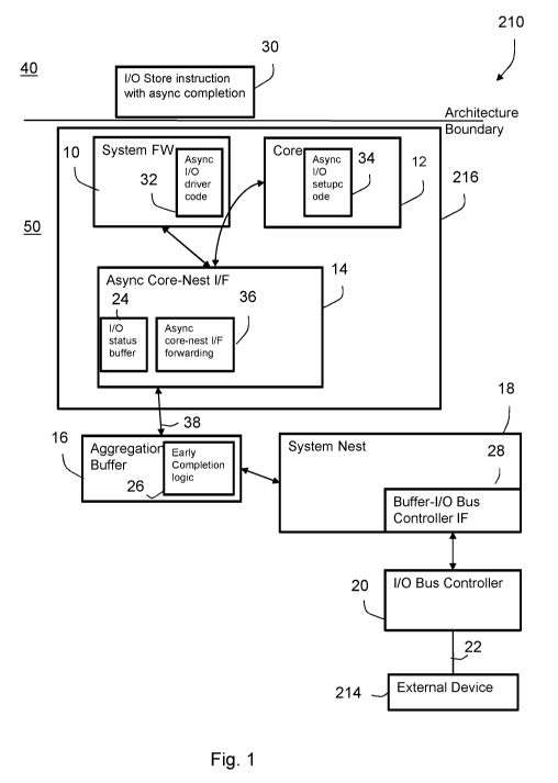
quiesce operation applicable to one zone (a target zone), processors outside
of the target
zone are permitted to continue running, although new translations may be
blocked.
Typically, at least one system controller or other mechanism broadcasts the
quiesce to all
physical processors in the sys- tem, handles collecting quiesce state
information and
indicates to a requesting processor when all processors have started, or are
ignoring
(filtering) the quiesce request.
[0007] A quiesce controller can be communicatively coupled to a
processor in a
multi-processor system, and a quiesce state machine configured to receive a
quiesce
request. The computer system is configured to perform a method that includes
receiving
a quiesce request at the quiesce controller from a requesting processor, the
requesting
processor being one of a plurality of processors in a multi-processor system,
and
determining that the quiesce request is not accepted based on a state of the
quiesce state
machine. The method also includes, based on the request being not accepted,
generating
a reject message configured to indicate that the quiesce request has been
rejected, holding
the reject message lmtil a quiesce command is broadcast to the multi-processor
system,
the quiesce command based on a different quiesce request, and sending the
reject
message to the requesting processor based on the broadcast of the quiesce
command
being detected by the quiesce controller.
2
CA 03127852 2021-07-26
WO 2020/156796 PCT/EP2020/050755
SUMMARY
[0008] A data processing system is proposed for handling an
input/output store
instruction, comprising a system nest communicatively coupled to at least one
input/output bus by an input/output bus controller. The data processing system
further
comprises at least a data processing unit comprising a core,
a system firmware and an asynchronous core-nest interface. The data processing
unit is
communicatively coupled to the system nest via an aggregation buffer. The
system nest is
configured to asynchronously load from and/or store data to at least one
external device
which is communicatively coupled to the input/output bus.
[0009] The data processing system is configured to perform: (i) an
operating system
running on the data processing system issues the input/output store
instruction specifying
at least an input/output function with an offset through an address, data to
be transferred
and/or a pointer to data to be transferred, and a length of the data; (ii) the
data processing
unit is configured to identify the input/output function by the address
specified in the
input/output store instruction; (iii) the data processing unit is configured
to verify if
access to the input/output function is allowed on an address space and on a
guest instance
level, the guest running on the data processing system; (iv) the data
processing unit is
configured to complete the input/output store instruction before an execution
of the
input/output store instruction in the system nest is completed; and (v) the
system
firmware is configured to notify the operating system through an interrupt, if
during the
asynchronous execution of the input/output store instruction an error is
detected by the
data processing unit, transmitting the data of the failed asynchronous
execution.
[0010] Favorably a number of cycles per instruction may be improved by
replacing a
synchronous PCI instruction by a reliable asynchronous send instruction and
mechanism.
A PCI store instruction with asynchronous execution of the PCIe store effect
and
asynchronous status handling may be performed. Asynchronous reliable execution
is
based on reliable forwarding mechanisms in microarchitecture.
[0011] The data processing system according to a first embodiment of
the invention
comprises instructions loading from and storing to at least one external
device of the data
processing system via an input/output bus. Asynchronous instructions complete
before
3
CA 03127852 2021-07-26
WO 2020/156796 PCT/EP2020/050755
data has been stored to the external device while synchronous instructions
complete after
data has been stored to the external device. Within the embodiments described
here, PCI
will be used interchangeably for any other input/output technology, thus not
restricting
the embodiment of the invention to PCI.
[0012] Embodiments of the invention describe an input/output store
instruction
execution in a strictly ordered way as observable from above the architecture
boundary
while the actual execution may be out of order within the hardware of the data
processing
unit (CPU).
[0013] According to embodiments of the invention a PCI store
instruction may be
executed with an asynchronous execution of the PCIe store effect and an
asynchronous
status handling. Asynchronous reliable execution is based on reliable
forwarding
mechanisms in microarchitecture of the inventive data processing system.
[0014] An existing PCI store and store block instruction is usually
synchronous up to
the point where the PCI store data has been delivered to the PCIe interface
and
completion returned to a processing unit.
[0015] PCI standard only requires an asynchronous send command of PCI
information, which is typically implemented through a store queue in the
processor
aggregating data with asynchronous send-out.
[0016] Advantageously, according to embodiments of the invention, an
improvement
concerning cycles per instruction may be achieved by replacing a synchronous
PCI
instruction by a reliable asynchronous send process of an input/output store
instruction.
[0017] Alternatively or additionally of data to be transferred, the
store instruction
according to an embodiment of the invention may also specify a pointer to a
main
memory which should be used to fetch data from, instead of containing the data
directly.
[0018] Guest instance level may also mean that a single guest or host
may be
running on the data processing system.
4
CA 03127852 2021-07-26
WO 2020/156796 PCT/EP2020/050755
[0019] The address of the offset of the input/output function itself
can be a virtual,
physical, logical address. Virtual and logical addresses typically get
translated through a
memory management unit (MMU) into a physical address, and the physical address
then
allows to identify which function and offset is meant.
[0020] Physical address in this context means "lowest address in the
address
translation hierarchy accessible from within a guest/operating system".
[0021] According to a favourable embodiment of the inventive data
processing
system, the aggregation buffer may be communicatively coupled to the
asynchronous
core-nest interface. Thus the aggregation buffer can handle data directly sent
by the
asynchronous core-nest interface consecutively until all data to be
transferred to the
external device are stored in the aggregation buffer.
[0022] According to a favourable embodiment of the inventive data
processing
system, the data may be transferred by the input/output store instruction
through an
asynchronous transmit mechanism with an early completion message in multiple
data
packets to the aggregation buffer, if the length of the source data exceeds
eight bytes, else
the data may be transferred in one data packet. The asynchronous transmit
mechanism is
favourable because the sending device is free for reuse at an earlier state.
[0023] According to a favourable embodiment of the inventive data
processing
system, the system firmware may comprise an asynchronous input/output driver
code for
handling the input/output store instruction. Thus an asynchronous transmit
mechanism
may be used for transferring data from the data processing unit to the
external device.
[0024] According to a favourable embodiment of the inventive data
processing
system, the core may comprise an asynchronous setup code for handling memory
requirements for status information of the asynchronous input/output driver
code. This
asynchronous setup code may further facilitate the asynchronous transmit
mechanism
through the aggregation buffer to the system nest and the input/output bus
controller.
[0025] According to a favourable embodiment of the inventive data
processing
system, the asynchronous core-nest interface may comprise an asynchronous core-
nest
5
CA 03127852 2021-07-26
WO 2020/156796 PCT/EP2020/050755
interface forwarding component for forwarding the data with local completion.
This
component may be implemented in hardware in the asynchronous core-nest
interface.
Thus a favourable asynchronous transmit mode for sending the data in data
packets to the
aggregation buffer may be supported.
[0026] According to a favourable embodiment of the inventive data
processing
system, the aggregation buffer may comprise an early completion logic for
delivering a
free for reuse message after sending a request. This enables an early
continuation of the
transmit process of the data via the aggregation buffer to the system nest and
the
input/output bus controller.
[0027] According to a favourable embodiment of the inventive data
processing
system, the aggregation buffer may be coupled to the asynchronous core-nest
interface
via an asynchronous bus. By this way the asynchronous transmit mechanism for
data
transfer from the asynchronous core-nest interface may be favourably
supported.
[0028] According to a favourable embodiment, the inventive data
processing system
may further comprise an input/output status buffer collecting returned states
from the
system nest and/or from the input/output bus controller, in particular a
completion
message from the system nest. This input/output status buffer collects the
returned states
acting as an asynchronous system message buffer supporting the asynchronous
transmit
process.
[0029] According to a favourable embodiment of the inventive data
processing
system, the asynchronous core-nest interface may comprise the input/output
status buffer.
Advantageously the input/output status buffer is integrated directly in the
asynchronous
core-nest interface for quick response.
[0030] According to a favourable embodiment of the inventive data
processing
system, a system message may comprise one of - a hierarchical physical target
address, -
sourcing an SMT (simultaneous multithreading) thread or an aggregate buffer
identifier, -
a length of data, an input/output bus address, or - a sequence number for a
recovery
algorithm. Thus an advantageous passing of relevant information through the
data
processing system can be guaranteed.
6
CA 03127852 2021-07-26
WO 2020/156796 PCT/EP2020/050755
[0031] Further a method is proposed for handling an input/output store
instruction to
at least one external device of a data processing system, the data processing
system
comprising a system nest communicatively coupled to at least one input/output
bus by an
input/output bus controller. The data processing system further comprises at
least a data
processing unit comprising a core, a system firmware and an asynchronous core-
nest
interface. The data processing unit is communicatively coupled to the system
nest via an
aggregation buffer. The external device is communicatively coupled to the
input/output
bus.
[0032] The method comprises: (i) an operating system running on the
data
processing system issuing the input/output store instruction specifying at
least an
input/output function with an offset through an address, data to be
transferred and/or a
pointer to data to be transferred, and a length of the data; (ii) the data
processing unit
being configured to identify the input/output function by the address
specified in the
input/output store instruction; (iii) the data processing unit being
configured to verify if
access to the input/output function is allowed on an address space and on a
guest instance
level, the guest running on the data processing system; (iv) the data
processing unit being
configured to complete the input/output store instruction before an execution
of the
input/output store instruction in the system nest is completed; and (v) the
system
firmware being configured to notify the operating system through an interrupt,
if during
the asynchronous execution of the input/output store instruction an error is
detected by
the data processing unit, transmitting the data of the failed asynchronous
execution.
[0033] Favorably a number of cycles per instruction may be improved by
replacing a
synchronous PCI instruction by a reliable asynchronous send instruction and
mechanism.
A PCI store instruction with asynchronous execution of the PCIe store effect
and
asynchronous status handling may be performed. Asynchronous reliable execution
is
based on reliable forwarding mechanisms in microarchitecture.
[0034] The method according to a further embodiment of the invention
comprises
instructions loading from and storing to at least one external device of the
data
processing system via an input/output bus. Asynchronous instructions complete
before
data has been stored to the external device while synchronous instructions
complete after
7
CA 03127852 2021-07-26
WO 2020/156796 PCT/EP2020/050755
data has been stored to the external device. Within the embodiments described
here, PCI
will be used interchangeably for any other input/output technology, thus not
restricting
the embodiment of the invention to PCI.
[0035] Embodiments of the inventive method describe an input/output store
instruction execution in a strictly ordered way as observable from above the
architecture
boundary while the actual execution may be out of order within the hardware of
the data
processing unit (CPU).
[0036] According to embodiments of the inventive method a PCI store
instruction
may be executed with an asynchronous execution of the PCIe store effect and an
asynchronous status handling. Asynchronous reliable execution is based on
reliable
forwarding mechanisms in microarchitecture of the inventive data processing
system.
[0037] An existing PCI store and store block instruction is usually
synchronous up to
the point where the PCI store data has been delivered to the PCIe interface
and
completion returned to a processing unit.
[0038] PCI standard only requires an asynchronous send command of PCI
information, which is typically implemented through a store queue in the
processor
aggregating data with asynchronous send-out.
[0039] Advantageously, according to embodiments of the inventive
method, an
improvement concerning cycles per instruction may be achieved by replacing a
synchronous PCI instruction by a reliable asynchronous send process of an
input/output
store instruction.
[0040] Alternatively or additionally of data to be transferred, the
store instruction
according to an embodiment of the invention may also specify a pointer to a
main
memory which should be used to fetch data from, instead of containing the data
directly.
[0041] Guest instance level may also mean that a single guest or host
may be
running on the data processing system.
8
CA 03127852 2021-07-26
WO 2020/156796 PCT/EP2020/050755
[0042] The address of the offset of the input/output function itself
can be virtual,
physical, logical address. Virtual and logical addresses typically get
translated through a
memory management unit (MMU) into a physical address, and the physical address
then
allows to identify which function and offset is meant.
[0043] Physical address in this context means "lowest address in the
address
translation hierarchy accessible from within a guest/operating system".
[0044] According to a favourable embodiment, the method may further
comprise: (i)
the operating system issuing the input/output store instruction; (ii)
depending on the
length of the data: if a length of the data exceeds eight bytes, the system
firmware issuing
repeatedly a system message to send a data packet to the aggregation buffer
until all data
of a store block have been forwarded to the aggregation buffer, while the
system
firmware waiting until the data have been sent by the system message; else the
system
firmware issuing a system message to send the data to the aggregation buffer;
further
independent of the length of the data, (iii) the system firmware issuing a
system message
to the aggregation buffer to forward the data asynchronously as single nest
message to
the input/output bus controller, while waiting for the aggregation buffer to
send a
completion message; (iv) the aggregation buffer injecting the nest message
into the
system nest, wherein the aggregation buffer is free for reuse right after the
send
operation, signaling back to the system firmware; then the aggregation buffer
sending a
free for reuse message; (v) the system nest forwarding the message to the
target location;
(vi) the input/output bus controller receiving the message and forwarding data
in a data
frame to the input/output bus; (vii) the input/output bus controller sending a
completion
message to the system nest; (viii) the system nest forwarding the completion
message to
the originating aggregation buffer; (ix) the aggregation buffer forwarding
completion to
the asynchronous core-nest interface; (x) the asynchronous core-nest interface
signaling
completion of operation to the system firmware; and (xi) the system firmware
signaling
asynchronously defects to the operating system in case of an error.
[0045] Only step (ii) is dependent on the length of the data and is
different for the
length of the data exceeding eight bytes from the length of the data not
exceeding eight
bytes.
9
CA 03127852 2021-07-26
WO 2020/156796 PCT/EP2020/050755
[0046] According to the embodiment of the inventive method, the data
are
transmitted in slices to the aggregation buffer until all data of a store
block are forwarded
to the aggregation buffer, wherein the system firmware is waiting until the
data has been
sent by the asynchronous core-nest interface.
[0047] Thus if data is less than eight bytes the filling process of the
aggregation
buffer in slices with data packets may be skipped and the transmit process of
the data to
the external device can be completed in a single step.
[0048] According to a favourable embodiment of the inventive method, the
data may
be transferred by the input/output store instruction through an asynchronous
transmit
mechanism with an early completion message in multiple data packets to the
aggregation
buffer, if the length of the data exceeds eight bytes. The asynchronous
transmit
mechanism is favourable because the sending device is free for reuse at an
earlier state.
[0049] According to a favourable embodiment of the inventive method,
the system
firmware may use an asynchronous input/output driver code for handling the
input/output
store instruction. Thus an asynchronous transmit mechanism may be used for
transferring
data from the data processing unit to the external device.
[0050] According to a favourable embodiment of the inventive method,
the core may
use an asynchronous setup code for handling memory requirements for status
information of the asynchronous input/output driver code. This asynchronous
setup code
may further facilitate the asynchronous transmit mechanism through the
aggregation
buffer to the system nest and the input/output bus controller.
[0051] According to a favourable embodiment of the inventive method,
the
asynchronous core-nest interface may use an asynchronous core-nest interface
forwarding component for forwarding the data with local completion. Thus a
favourable
asynchronous transmit mode for sending the data in data packets to the
aggregation
buffer may be supported.
[0052] According to a favourable embodiment of the inventive method,
the
aggregation buffer may use an early completion logic for delivering a free for
reuse
CA 03127852 2021-07-26
WO 2020/156796 PCT/EP2020/050755
message after sending a request. This enables an early continuation of the
transmit
process of the data via the aggregation buffer to the system nest and the
input/output bus
controller.
[0053] According to a favourable embodiment of the inventive method, an
input/output status buffer may collect returned states from the system nest
and/or from
the input/output bus controller, in particular a completion message from the
system nest.
This input/output status buffer collects the returned states acting as an
asynchronous
system message buffer supporting the asynchronous transmit process.
[0054] According to a favourable embodiment of the inventive method, a
system
message may comprise one of - a hierarchical physical target address, -
sourcing an SMT
thread or an aggregate buffer identifier, - a length of data, - an
input/output bus address,
or - a sequence number for a recovery algorithm. Thus an advantageous passing
of
relevant information through the data processing system can be guaranteed.
[0055] Further, a favorable computer program product is proposed for
handling an
input/output store instruction to at least one external device of a data
processing system,
the data processing system comprising a system nest communicatively coupled to
at least
one input/output bus by an input/output bus controller. The data processing
system
further comprises at least a data processing unit comprising a core, a system
firmware
and an asynchronous core-nest interface. The data processing unit is
communicatively
coupled to the system nest via an aggregation buffer. The external device is
communicatively coupled to the input/output bus.
[0056] The computer program product comprises a computer readable
storage
medium having program instructions embodied therewith, the program
instructions
executable by the computer system to cause the computer system to perform a
method
comprising: (i) an operating system running on the data processing system
issuing the
input/output store instruction specifying at least an input/output function
with an offset
through an address, data to be transferred and/or a pointer to data to be
transferred, and a
length of the data; (ii) the data processing unit being configured to identify
the
input/output function by the address specified in the input/output store
instruction; (iii)
the data processing unit being configured to verify if access to the
input/output function
11
CA 03127852 2021-07-26
WO 2020/156796 PCT/EP2020/050755
is allowed on an address space and on a guest instance level, the guest
running on the
data processing system; (iv) the data processing unit being configured to
complete the
input/output store instruction before an execution of the input/output store
instruction in
the system nest is completed; and (v) the system firmware being configured to
notify the
operating system through an interrupt, if during the asynchronous execution of
the
input/output store instruction an error is detected by the data processing
unit, transmitting
the data of the failed asynchronous execution.
[0057] Further, a data processing system for execution of a data
processing program
is proposed, comprising computer readable program instructions for performing
the
method described above.
BRIEF DESCRIPTION OF THE SEVERAL VIEWS OF THE DRAWINGS
[0058] The present invention together with the above-mentioned and
other objects
and advantages may best be understood from the following detailed description
of the
embodiments, but not restricted to the embodiments.
[0059] Figure 1 depicts a block diagram of a data processing system for
handling an
input/output store instruction to an external device according to an
embodiment of the
invention.
[0060] Figure 2 depicts a message sequence chart of a method for
handling an
input/output store instruction to an external device according to an
embodiment of the
invention.
[0061] Figure 3 depicts a flow chart for handling an input/output store
instruction to
an external device according to an embodiment of the invention.
[0062] Figure 4 depicts an example embodiment of a data processing
system for
executing a method according to the invention.
12
CA 03127852 2021-07-26
WO 2020/156796 PCT/EP2020/050755
DETAILED DESCRIPTION
[0063] In the drawings, like elements are referred to with equal
reference numerals.
The drawings are merely schematic representations, not intended to portray
specific
parameters of the invention. Moreover, the drawings are intended to depict
only typical
embodiments of the invention and therefore should not be considered as
limiting the
scope of the invention.
[0064] The illustrative embodiments described herein provide a data
processing
system and a method for handling an input/output store instruction, comprising
a system
nest communicatively coupled to at least one input/output bus by an
input/output bus
controller. The data processing system further comprises at least a data
processing unit
comprising a core, a system firmware and an asynchronous core-nest interface.
The data
processing unit is communicatively coupled to the system nest via an
aggregation buffer.
The system nest is configured to asynchronously load from and/or store data to
at least
one external device which is communicatively coupled to the input/output bus.
[0065] The illustrative embodiments may be used for the method
comprising: (i) an
operating system running on the data processing system issues the input/output
store
instruction specifying at least an input/output function with an offset
through an address,
data to be transferred and/or a pointer to data to be transferred, and a
length of the data;
(ii) the data processing unit is configured to identify the input/output
function by the
address specified in the input/output store instruction; (iii) the data
processing unit is
configured to verify if access to the input/output function is allowed on an
address space
.. and on a guest instance level, the guest running on the data processing
system; (iv) the
data processing unit is configured to complete the input/output store
instruction before an
execution of the input/output store instruction in the system nest is
completed; and (v) the
system firmware is configured to notify the operating system through an
interrupt, if
during the asynchronous execution of the input/output store instruction an
error is
detected by the data processing unit, transmitting the data of the failed
asynchronous
execution.
[0066] Alternatively or additionally of data to be transferred, the
store instruction
according to an embodiment of the invention may also specify a pointer to main
memory
13
CA 03127852 2021-07-26
WO 2020/156796 PCT/EP2020/050755
which should be used to fetch data from, instead of containing the data
directly.
[0067] Guest instance level may also mean that a single guest or host
may be
running on the data processing system.
[0068] The address of the offset of the input/output function itself
can be virtual,
physical, logical address. Virtual and logical addresses typically get
translated through a
memory management unit (MMU) into a physical address, and the physical address
then
allows to identify which function and offset is meant.
[0069] Physical address in this context means "lowest address in the
address
translation hierarchy accessible from within a guest/operating system".
[0070] Figure 1 depicts a block diagram of a data processing system 210
for
handling an input/output store instruction 30 to at least one external device
214 according
to an embodiment of the invention. The data processing system 210 comprises a
system
nest 18 communicatively coupled to an input/output bus 22 by an input/output
bus
controller 20, a data processing unit 216 comprising a core 12, a system
firmware 10 and
an asynchronous core-nest interface 14.
[0071] The data processing unit 216 is communicatively coupled to the
system nest
18 via an aggregation buffer 16. The system nest 18 is configured to
asynchronously load
from and/or store data to the external device 214 which is communicatively
coupled to
the input/output bus 22 via a buffer-input/output bus controller interface 28
as part of the
system nest 18 and the input/output bus controller 28.
[0072] The aggregation buffer 16 is communicatively coupled to the
asynchronous
core-nest interface 14. The system firmware 10 comprises an asynchronous
input/output
driver code 32 for handling the input/output store instruction 30. The core 12
comprises
an asynchronous setup code 34 for handling memory requirements for status
information
of the asynchronous input/output driver code 32. The asynchronous core-nest
interface
14 comprises an asynchronous core-nest interface forwarding component 36 for
forwarding the data with local completion. The aggregation buffer 16 comprises
an early
completion logic 26 for delivering a free for reuse message after sending a
request. The
14
CA 03127852 2021-07-26
WO 2020/156796
PCT/EP2020/050755
aggregation buffer 16 is coupled to the asynchronous core-nest interface 14
via an
asynchronous bus 38. An input/output status buffer 24 is comprised, collecting
returned
states from the system nest 18 and/or from the input/output bus controller 20,
in
particular a completion message from the system nest 18. The input/output
status buffer
24 is integrated directly in the asynchronous core-nest interface 14.
[0073] According to an embodiment of the inventive method, an operating
system
running on the data processing system 210 issues the input/output store
instruction 30
specifying at least an input/output function with an offset through an
address, data to be
transferred and/or a pointer to data to be transferred, and a length of the
data. The data
processing unit 216 is hereby configured to identify the input/output function
by the
address specified in the input/output store instruction 30. The data
processing unit 216 is
configured to verify if access to the input/output function is allowed on an
address space
and on a guest instance level, the guest running on the data processing system
210. The
data processing unit 216 is configured to complete the input/output store
instruction 30
before an execution of the input/output store instruction 30 in the system
nest 18 is
completed. The system firmware 10 is configured to notify the operating system
through
an interrupt, if during the asynchronous execution of the input/output store
instruction 30
an error is detected by the data processing unit 216, transmitting the data of
the failed
asynchronous execution.
[0074] The input/output store instruction 30 is located in the data
processing system
210 on the side of the user interface 40 across the architecture boundary
which separates
the system hardware/firmware 50 from the user side 40.
[0075] Thus the data are transferred by the input/output store
instruction 30 through
an asynchronous transmit mechanism with an early completion message in
multiple data
packets to the aggregation buffer 16, if the length of the source data exceeds
eight bytes,
else the data are transferred in one data packet.
[0076] A system message according to an embodiment of the inventive
data
processing system comprises one of a hierarchical physical target address,
sourcing an
SMT thread or an aggregate buffer identifier, a length of data, an
input/output bus
address, or a sequence number for a recovery algorithm.
CA 03127852 2021-07-26
WO 2020/156796 PCT/EP2020/050755
[0077] Figure 2 depicts a message sequence chart of the method for
handling an
input/output store instruction 30 to an external device 214 according to an
embodiment
of the invention.
[0078] As shown in Figure 2 the method starts with, the operating
system issuing the
input/output store instruction 30. Next, as is indicated by the steps S100 and
S104, the
system firmware 10 issues repeatedly, if a length of the data exceeds eight
bytes, a
system message to send a data packet to the aggregation buffer 16 until all
data of a store
block have been forwarded to the aggregation buffer 16, while the system
firmware 10 is
waiting until the data have been sent by the system message. In steps S102 and
S106 a
local completion message is sent back to the system firmware 10.
[0079] Then in step S108, the system firmware 10 issues a system
message to the
aggregation buffer 16 to forward the data asynchronously as single nest
message to the
input/output bus controller 20, while waiting for the aggregation buffer 16 to
send a
completion message.
[0080] Next in step 5110, the aggregation buffer 16 injects the nest
message into the
system nest 18, wherein the aggregation buffer 16 is free for reuse right
after the send
operation, signaling back to the system firmware 10. Then the aggregation
buffer 16
sends a free for reuse message.
[0081] In step S112, the system nest 18 forwards the message to the
target location,
followed by step S114, the input/output bus controller 20 receiving the
message and
forwarding data in a data frame to the input/output bus, followed by the
input/output bus
controller 20 sending a completion message to the system nest 18 in step S116.
[0082] Next in step S118, the system nest 18 forwards the completion
message to the
originating aggregation buffer 16, followed by the aggregation buffer 16
forwarding
completion to the asynchronous core-nest interface 14 in step S120. Then in
step S122
the asynchronous core-nest interface 14 signals completion of operation to the
system
firmware 10.
16
CA 03127852 2021-07-26
WO 2020/156796 PCT/EP2020/050755
[0083] In case of an error occurring during transfer of data, the
system firmware 10
signals asynchronously defects to the operating system.
[0084] In case, the data to be transferred are less than eight bytes,
the repeatedly
filling of the aggregation buffer 16 is skipped.
[0085] Figure 3 depicts a flow chart for handling an input/output store
instruction 30
to an external device 214 according to an embodiment of the invention.
[0086] The system firmware of the data processing unit starts in step S200.
In step
S202 the system firmware receives an input/output store block instruction.
[0087] Then in step S204 it is checked if the more than 8 bytes are to
be transferred.
If this is the case the core-nest interface fills the aggregation buffer with
an up to 16 bytes
message in step S206. The system firmware is waiting, step S208, until a
message of
local completion is sent in step S210, returning to step S204. If there are
less than 8 bytes
left in the check of step S204, the flow continues in step S212 with the core-
nest
interface sending an asynchronous input/output message, followed by waiting in
step
S214 for a buffer response in step S216. Then in step S218 a finish store
block
instruction is executed and the flow ends in step S220 with an ending in the
system
firmware.
[0088] In step S228 the asynchronous core-nest interface logic starts
an outbound
process loop, followed by receiving an aggregation buffer completion message
in step
S222 and a forward data message to the aggregation buffer in step S224,
followed by a
send completion message back to the system firmware in step S226. In step S230
an
asynchronous input/output send message is received followed by a forward of
the
input/output send message to the aggregation buffer.
[0089] In step S238 the aggregation buffer logic starts an outbound process
loop
followed by a receive data in step S234 and aggregating data in the
aggregation buffer in
step S236. The aggregation buffer is also receiving an input/output send
message in step
S240, followed by forwarding data from the aggregation buffer with an
input/output send
message in step S242. Next in step S244 a response message from the
aggregation buffer
17
CA 03127852 2021-07-26
WO 2020/156796 PCT/EP2020/050755
is sent via the core-nest interface to the system firmware.
[0090] Referring now to Figure 4, a schematic of an example of a data
processing
system 210 is shown. Data processing system 210 is only one example of a
suitable data
processing system and is not intended to suggest any limitation as to the
scope of use or
functionality of embodiments of the invention described herein. Regardless,
data
processing system 210 is capable of being implemented and/or performing any of
the
functionality set forth herein above.
[0091] In data processing system 210 there is a computer system/server 212,
which
is operational with numerous other general-purpose or special-purpose
computing system
environments or configurations. Examples of well-known computing systems,
environments, and/or configurations that may be suitable for use with computer
system/server 212 include, but are not limited to, personal computer systems,
server
computer systems, thin clients, thick clients, handheld or laptop devices,
multiprocessor
systems, microprocessor-based systems, set top boxes, programmable consumer
electronics, network PCs, minicomputer systems, mainframe computer systems,
and
distributed cloud computing environments that include any of the above systems
or
devices, and the like.
[0092] Computer system/server 212 may be described in the general
context of
computer system executable instructions, such as program modules, being
executed by a
computer system. Generally, program modules may include routines, programs,
objects,
components, logic, data structures, and so on that perform particular tasks or
implement
particular abstract data types. Computer system/server 212 may be practiced in
distributed cloud computing environments where tasks are performed by remote
processing devices that are linked through a communications network. In a
distributed
cloud computing environment, program modules may be located in both local and
remote
computer system storage media including memory storage devices.
[0093] As shown in Fig. 4, computer system/server 212 in data
processing system
210 is shown in the form of a general-purpose computing device. The components
of
computer system/server 212 may include, but are not limited to, one or more
processors
or processing units 216, a system memory 228, and a bus 218 that couples
various
18
CA 03127852 2021-07-26
WO 2020/156796 PCT/EP2020/050755
system components including system memory 228 to processor 216.
[0094] Bus 218 represents one or more of any of several types of bus
structures,
including a memory bus or memory controller, a peripheral bus, an accelerated
graphics
port, and a processor or local bus using any of a variety of bus
architectures. By way of
example, and not limitation, such architectures include Industry Standard
Architecture
(ISA) bus, Micro Channel Architecture (MCA) bus, Enhanced ISA (EISA) bus,
Video
Electronics Standards Association (VESA) local bus, and Peripheral Component
Interconnect (PCI) bus.
[0095] Computer system/server 212 typically includes a variety of
computer system
readable media. Such media may be any available media that is accessible by
computer
system/server 212, and it includes both volatile and non-volatile media,
removable and
non-removable media.
[0096] System memory 228 can include computer system readable media in
the
form of volatile memory, such as random access memory (RAM) 230 and/or cache
memory 232. Computer system/server 212 may further include other removable/non-
removable, volatile/non-volatile computer system storage media. By way of
example
only, storage system 234 can be provided for reading from and writing to a non-
removable, non-volatile magnetic media (not shown and typically called a "hard
drive").
Although not shown, a magnetic disk drive for reading from and writing to a
removable,
non-volatile magnetic disk (e.g., a "floppy disk"), and an optical disk drive
for reading
from or writing to a removable, non-volatile optical disk such as a CD-ROM,
DVD-
ROM or other optical media can be provided. In such instances, each can be
connected to
bus 218 by one or more data media interfaces. As will be further depicted and
described
below, memory 228 may include at least one program product having a set (e.g.,
at least
one) of program modules that are configured to carry out the functions of
embodiments
of the invention.
[0097] Program/utility 240, having a set (at least one) of program
modules 242, may
be stored in memory 228 by way of example, and not limitation, as well as an
operating
system, one or more application programs, other program modules, and program
data.
Each of the operating system, one or more application programs, other program
modules,
19
CA 03127852 2021-07-26
WO 2020/156796 PCT/EP2020/050755
and program data or some combination thereof, may include an implementation of
a
networking environment. Program modules 242 generally carry out the functions
and/or
methodologies of embodiments of the invention as described herein.
[0098] Computer system/server 212 may also communicate with one or more
external devices 214 such as a keyboard, a pointing device, a display 224,
etc.; one or
more devices that enable a user to interact with computer system/server 212;
and/or any
devices (e.g., network card, modem, etc.) that enable computer system/server
212 to
communicate with one or more other computing devices. Such communication can
occur
via Input/Output (I/O) interfaces 222. Still yet, computer system/server 212
can
communicate with one or more networks such as a local area network (LAN), a
general
wide area network (WAN), and/or a public network (e.g., the Internet) via
network
adapter 220. As depicted, network adapter 220 communicates with the other
components
of computer system/server 212 via bus 218. It should be understood that
although not
shown, other hardware and/or software components could be used in conjunction
with
computer system/server 212. Examples, include, but are not limited to:
microcode,
device drivers, redundant processing units, external disk drive arrays, RAID
systems,
tape drives, and data archival storage systems, etc.
[0099] The present invention may be a system, a method, and/or a computer
program product. The computer program product may include a computer readable
storage medium (or media) having computer readable program instructions
thereon for
causing a processor to carry out aspects of the present invention.
[00100] The computer readable storage medium can be a tangible device that
can
retain and store instructions for use by an instruction execution device. The
computer
readable storage medium may be, for example, but is not limited to, an
electronic storage
device, a magnetic storage device, an optical storage device, an
electromagnetic storage
device, a semiconductor storage device, or any suitable combination of the
foregoing. A
non-exhaustive list of more specific examples of the computer readable storage
medium
includes the following: a portable computer diskette, a hard disk, a random
access
memory (RAM), a read-only memory (ROM), an erasable programmable read-only
memory (EPROM or Flash memory), a static random access memory (SRAM), a
portable compact disc read-only memory (CD-ROM), a digital versatile disk
(DVD), a
CA 03127852 2021-07-26
WO 2020/156796 PCT/EP2020/050755
memory stick, a floppy disk, a mechanically encoded device such as punch-cards
or
raised structures in a groove having instructions recorded thereon, and any
suitable
combination of the foregoing. A computer readable storage medium, as used
herein, is
not to be construed as being transitory signals per se, such as radio waves or
other freely
propagating electromagnetic waves, electromagnetic waves propagating through a
waveguide or other transmission media (e.g., light pulses passing through a
fiber-optic
cable), or electrical signals transmitted through a wire.
[00101] Computer readable program instructions described herein can be
downloaded
to respective computing/processing devices from a computer readable storage
medium or
to an external computer or external storage device via a network, for example,
the
Internet, a local area network, a wide area network and/or a wireless network.
The
network may comprise copper transmission cables, optical transmission fibers,
wireless
transmission, routers, firewalls, switches, gateway computers and/or edge
servers. A
network adapter card or network interface in each computing/processing device
receives
computer readable program instructions from the network and forwards the
computer
readable program instructions for storage in a computer readable storage
medium within
the respective computing/processing device.
[00102] Computer readable program instructions for carrying out operations
of the
present invention may be assembler instructions, instruction-set-architecture
(ISA)
instructions, machine instructions, machine dependent instructions, microcode,
firmware
instructions, state-setting data, or either source code or object code written
in any
combination of one or more programming languages, including an object oriented
programming language such as Smalltalk, C++ or the like, and conventional
procedural
programming languages, such as the "C" programming language or similar
programming
languages. The computer readable program instructions may execute entirely on
the
user's computer, partly on the user's computer, as a stand-alone software
package, partly
on the user's computer and partly on a remote computer or entirely on the
remote
computer or server. In the latter scenario, the remote computer may be
connected to the
user's computer through any type of network, including a local area network
(LAN) or a
wide area network (WAN), or the connection may be made to an external computer
(for
example, through the Internet using an Internet Service Provider). In some
embodiments, electronic circuitry including, for example, programmable logic
circuitry,
21
CA 03127852 2021-07-26
WO 2020/156796 PCT/EP2020/050755
field-programmable gate arrays (FPGA), or programmable logic arrays (PLA) may
execute the computer readable program instructions by utilizing state
information of the
computer readable program instructions to personalize the electronic
circuitry, in order to
perform aspects of the present invention.
[00103] Aspects of the present invention are described herein with
reference to
flowchart illustrations and/or block diagrams of methods, apparatus (systems),
and
computer program products according to embodiments of the invention. It will
be
understood that each block of the flowchart illustrations and/or block
diagrams, and
combinations of blocks in the flowchart illustrations and/or block diagrams,
can be
implemented by computer readable program instructions.
[00104] These computer readable program instructions may be provided to
a
processor of a general-purpose computer, special-purpose computer, or other
programmable data processing apparatus to produce a machine, such that the
instructions, which execute via the processor of the computer or other
programmable
data processing apparatus, create means for implementing the functions/acts
specified in
the flowchart and/or block diagram block or blocks. These computer readable
program
instructions may also be stored in a computer readable storage medium that can
direct a
computer, a programmable data processing apparatus, and/or other devices to
function in
a particular manner, such that the computer readable storage medium having
instructions
stored therein comprises an article of manufacture including instructions
which
implement aspects of the function/act specified in the flowchart and/or block
diagram
block or blocks.
[00105] The computer readable program instructions may also be loaded
onto a
computer, other programmable data processing apparatus, or other device to
cause a
series of operational steps to be performed on the computer, other
programmable
apparatus or other device to produce a computer implemented process, such that
the
instructions which execute on the computer, other programmable apparatus, or
other
device implement the functions/acts specified in the flowchart and/or block
diagram
block or blocks.
[00106] The flowchart and block diagrams in the Figures illustrate the
architecture,
22
CA 03127852 2021-07-26
WO 2020/156796
PCT/EP2020/050755
functionality, and operation of possible implementations of systems, methods,
and
computer program products according to various embodiments of the present
invention.
In this regard, each block in the flowchart or block diagrams may represent a
module,
segment, or portion of instructions, which comprises one or more executable
instructions
for implementing the specified logical function(s). In some alternative
implementations,
the functions noted in the block may occur out of the order noted in the
figures. For
example, two blocks shown in succession may, in fact, be executed
substantially
concurrently, or the blocks may sometimes be executed in the reverse order,
depending
upon the functionality involved. It will also be noted that each block of the
block
diagrams and/or flowchart illustration, and combinations of blocks in the
block diagrams
and/or flowchart illustration, can be implemented by special-purpose hardware-
based
systems that perform the specified functions or acts or carry out combinations
of special-
purpose hardware and computer instructions.
[00107] The descriptions of the various embodiments of the present
invention have
been presented for purposes of illustration, but are not intended to be
exhaustive or
limited to the embodiments disclosed. Many modifications and variations will
be
apparent to those of ordinary skill in the art without departing from the
scope and spirit
of the described embodiments. The terminology used herein was chosen to best
explain
.. the principles of the embodiments, the practical application or technical
improvement
over technologies found in the marketplace, or to enable others of ordinary
skill in the art
to understand the embodiments disclosed herein.
23
CA 03127852 2021-07-26
WO 2020/156796
PCT/EP2020/050755
REFERENCE NUMERALS
system FW
5 12 core
14 async core-nest IF
16 aggregation buffer
18 system nest
I/O bus controller
10 22 I/0 bus
24 I/O status buffer
26 early completion logic
28 buffer-I/O bus controller IF
I/O store instruction
15 32 async I/O driver code
34 I/O setup code
36 async forwarding
38 async bus
user IF
20 42
44
46
48
system HW/FW
210 data processing system
212 computer system/server
214 external devices
216 CPU / data processing unit
218 I/O Bus
220 network adapter
222 I/O interfaces
224 display
228 memory
24
CA 03127852 2021-07-26
WO 2020/156796
PCT/EP2020/050755
230 RAM
232 cache
234 storage system
240 program/utility
242 program modules